Note: Descriptions are shown in the official language in which they were submitted.
-~ ~ 21~28~9
SEI 96-18
TITLE OF THE lNv~NlION
DIAMOND-ZnO SURFACE ACOUSTIC WAVE DEVICE
BACKGROUND OF THE lNv~NllON
Field of the Invention
The present invention relates to an improved
surface acoustic wave (SAW) device which comprises ZnO
and diamond. The SAW device according to the present
invention is applicable in operating at higher
frequency.
Related Backqround Art
A surface acoustic wave device ~SAW device) is a
device which utilizes the acoustic wave propagation and
the piezoelectricity on the surface of particular solid
materials. The SAW device has excellent temperature
stability, durability, and phase characteristics.
Thus, there are certain demands, in the field of the
advanced communication technology, for SAW devices
- which can be used in high frequency bands of more than
2 GHz, such as band-stop filters, resonators, delay
devices, signal processing devices, convolvers, and
functional elements for opto-electronic devices. For
example, the band-stop filter with wider bandwidth is
necessary for the equipments for cellular
phones/communications which are typically operated in
high frequency bands of more than 2 GHz.
The SAW devices typically comprises interdigital
2i 8282g
SEI 96-18
transducers(IDT) for generating and detecting the
surface acoustic wave. The operation frequency(f) of a
SAW device is given by the equation :f = ~/ A,
- where V is the wave propagation velocity in the SAW
device, and A is the wavelength of the surface acoustic
wave. The operation frequency of more than 2 GHz is
required for SAW device to be used for the band-stop
filters with wider bandwidth. The wavelength 1 is
generally proportional to the width (d) of electrodes
of the interdigital transducer.
Because of difficulties on microfabrication
technique, the electrode with the width (d) of less
than 0.5 ~m is difficult to be obtained, thus it is
difficult to achieve desirable operation frequency (f)
of more than 2 GHz by decreasing wavelength A.
Therefore, the SAW device with higher propagation
velocity V is required for being applied to the
operation at the frequency of 2 GHz or higher.
The energy transform (piezoelectric) efficiency is
also important for SAW device to be used for the
advanced communication equipments. The effective
coupling coefficient(K2) is an index to conversion
efficiency of-the converting of electrical energy into
mechanical energy on the surface of the device. The
preferable range of the effective coupling coefficient
depends upon applications; about 0.15% - about 0.7% for
~ ` 2182823
SEI 96-18
narrow-band filter; about 0.7% - about 3% for medium-
band filter; and about 3% - about 6% for wide-band
filter.
The temperature coefficient for frequency (TCF) of
the SAW device is preferable to be small as possible,
because the smaller temperature dependency of the SAW
device is desirable. The propagation loss of the SAW
device is also preferable to be small as possible,
since smaller attenuation in propagation of surface
acoustic wave is desirable.
The theoretical and the experimental evaluation on
surface acoustic wave properties of SAW devices, which
includes ZnO for piezoelectric material and sAprhire,
is disclosed by Mitsuyu et.al.(Mitsuyu,T., S Ono and K
Wasa, J. Appl. Phys, 2464-2470,51(5), May 1980). The
reference teaches that the sapphire-ZnO SAW device can
be used for filter with 1050 MHz center frequency.
However, Mitsuyu did not teach the SAW device which can
be operated at the frequency of 3 MHz or higher.
Consequently, a different constitution of SAW device is
necessary for the operation at higher frequency.
Diamond is a material which have higher sonic
propagation properties than other materials for SAW
device, such as sapphire.
Figs. 2A to 2G illustrate the layer/electrode
constitution of SAW devices. In US Patent No.
~lg282~
SEI 96-18
5,446,329 to Nakahata et.al., propagation velocity V,
effective coupling coefficient R and temperature
coefficient with frequency TCF have been im~luved, in
particular by focusing first mode surface acoustic
wave: for example, V of 8,000 to 10,000 (m/s), TCF of -
10 to 10 (ppm/ C) and K2 of 0.7 to 1.7 (%) are achieved
for "type E" constitution shown in Fig. 2E; V of 8,000
to 10,000 (m/s), TCF of -10 to 10 (ppmi C) and K2 of 1
to 3 (%) are achieved for "type B" constitution shown
in Fig. 2B; V of 8,000 to 10,000 (m/s), TCF of -10 to
10 (ppm/C) and K2 of 1.5 to 4.5 (%) are achieved for
~type F" constitution shown in Fig. 2F; V of 8,000 to
10,000 (m/s), TCF of -10 to 10 (ppm/ C) and K of 0.8 to
2.3 (%) are achieved for "type D" constitution shown in
Fig. 2D; and V of 8,000 to 10,000 (m/s), TCF of -10 to
10 (ppm/ C) and K2 of 0.7 to 2.2 (%) are achieved for
"type G" constitution shown in Fig. 2G.
It is also kno~n that the performances of the SAW
device can be further improved by employing LiNbO3 or
LiTaO3 for piezoelectric material of SAW device.
Nevertheless, the use of ZnO for piezoelectric
material of SAW device can provide significant
advantage in fabricating SAW device, because film
formability of ZnO film onto diamond layer is much
better than LiNbO3 or LiTaO3 films. Therefore, it is
desirable to further improve the performances of SAW
~1~2~2Yi
SEI 96-18
device which comprise ZnO piezoelectric layer.
It is also desirable to further improve the
performances of the SAW devices in which short circuit
electrode, typically made of aluminum (Al), is not
included between diamond layer and ZnO layer, such as
"type A" and ntype C" devices shown in Fig. 2A and Fig.
2C, respectively. Because such device constitution
can eliminate the limitation on the process conditions
for forming ZnO layer such as process temperature,
since Al electrode having relatively low melting point
is not included.
Therefore, it is an object of the invention to
further improve the propagation velocity V, the
effective coupling coefficient K2, the thermal
coefficient for frequency TCF and propagation loss of
the SAW device which includes ZnO piezoelectric layer
formed on diamond layer, to provide SAW device having
improved operation characteristics at the frequency of
2 GHz or higher with superior durability and less
energy loss.
SUMMARY OF THE lNV~NlION
We have evaluated a number of experimental results
to obtain the desirable range of layer thickness which
provides desired operation frequency with less energy
loss, by using a dimensionless thickness khl, which is
defined as khz = 2~(tz/A)~ where tz (~m) is the thickness
~:1828~
SEI 96-18
of the piezoelectric material (ZnO) layer and A is the
wavelength of the surface acoustic wave. This
parameter is appropriate in the present invention for
determining the desirable thickness with the specified
wavelength propagating across the surface of SAW
device.
We have also evaluated a number of experimental
results to obtain the desirable range of the
passivating material (SiO2) layer thickness which
provides desired operation frequency with less energy
loss, by using a dimensionless thickness kh" which is
defined as kh. = 2~t./A), where t. (~m) is the thickness
of the SiO2 layer and 1 is the wavelength of the surface
acoustic wave. After the evaluation, we have
obtAine~ satisfactory result in the SAW devices having
layer/electrode constitutions shown in Figs. 2A (type
A), 2B (type B), 2C ttype C), 2D (type ~) and 2F (type
F).
The SAW devices according to the present invention
are provide with superior operating performances such
as propagation velocity (V), temperature coefficient
for frequency (TCF), effective coupling coefficient (K2)
and propagation loss. Such performances have not been
experienced for SAW devices having the layer/electrode
constitutions shown in Figs. 2A, 2B, 2C, 2D and 2F.
The first SAW device for 2nd mode surface acoustic
282g
SEI 96-18
wave of a wavelength A (~m) according to the present
invention comprises: (i) a diamond layer, (ii) a ZnO
layer formed on the diamond layer, the ZnO layer having
a thickness t~, (iii) an interdigital transducer (IDT)
formed over the ZnO layer, and (iv) a SiO2 layer formed
over the interdigital transducer onto the ZnO layer,
the SiO2 layer having a thickness of t.; wherein a
parameter kh~=(2~/A)t, and a parameter kh,=(2~/A)t. are
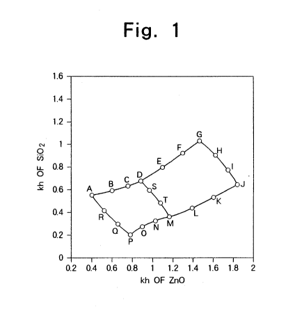
given within a region A-B-C-D-E-F-G-H-I-J-R-L-M-N-O-P-
Q-R-A in a two-dimensional Cartesian coordinate graph
having abscissa axis of khz and ordinate axis of kh.,
the outer edge of the region A-B-C-D-E-F-G-H-I-J-R-L-M-
N-O-P-Q-R-A being given by a closed chain in the
Cartesian coordinate, consisting of points A, B, C, D,
E, F, G, H, I, J, X, L, M, N, O, P, Q and R and lines
A-B, B-C, C-D, D-E, E-F, F-G, G-H, H-I, I-J, J-R, R-L,
L-M, M-N, N-O, O-P, P-Q, Q-R and R-A, the point A being
given by a coordinate point (khz=0.4, kh.=0.55); the
point B being given by a coordinate point (kh,=0.6,
kh.=0.6); the point C being given by a coordinate point
(khz=0.75, kh.=0.63); the point D being given by a
coordinate point (kh~=0.88, kh.=0.68); the point E being
given by a coordinate point (khS=l.1, kh.=0.8); the
point F being given by a coordinate point (khz=1.3,
kh.=0.93); the point G being given by a coordinate point
(kh~=1.47, kh.=1.03); the point H being given by a
~182823
SEI 96-18
coordinate point (kh~=1.61, kh.=0.92); the point I being
given by a coordinate point (kh~=1.75, kh,=0.77); the
point J being given by a coordinate point (kh~=1.82,
kh.=0.64); the point R being given by a coordinate point
(khS=1.6~ kh.=0.54); the point L being given by a
coordinate point ~kh,=1.41, kh.=0.42); the point M being
given by a coordinate point ~kh~=l.l9, kh,=0.35); the
point N being given by a coordinate point (kh~=1.03,
kh.=0.32); the point O being given ~y a coordinate point
(khS=0.92, kh.=0.28); the point P being given by a
coordinate point (kh~=0.8, kh,=0.2); the point Q being
given by a coordinate point (kh~=0.66, kh.=0.3); and the
point R being given by a coordinate point (kh~=0.53,
kh.=0.42). The layer structure of this SAW device is
schematically illustrated in Fig. 2A, "type A".
The SAW device having above constitution is
provided with propagation velocity V of from 8,000 to
12,000 (m/s), temperature coefficient for frequency TCF
of from -15 to 15 (ppm/C) and effective coupling
coefficient R of from 0.4 to 1.3 (%). The SAW device
is also provided with propagation loss of 0.05 (dB/~)
for 1st mode SAW, and 0.03 (dB/A) for 2nd mode SAW.
Further, such constitution has an advantage in
fabricating process.
The first surface acoustic wave device according to
the invention may have another constitution in which
21~2829
SEI 96-18
the parameter khS and kh. are given within a region A-B-
C-D-S-T-M-N-O-P-Q-R-A in the two-dimensional Cartesian
coordinate graph, the outer edge of the region A-B-C-D-
S-T-M-N-O-P-Q-R-A being given by a closed chain in the
Cartesian coordinate, consisting of the points A, B, C
and D, a point S, a point T, the points M, N, O, P, Q
and R and lines A-B, B-C, C-D, D-S, S-T, T-M, M-N, N-O,
O-P, P-Q, Q-R and R-A, the point S being given by a
coordinate point (khz=0.98, kh.=0.6); and the point T
being given by a coordinate point (kh,=l.1, kh.=0.5).
The SAW device having this constitution is provided
with propagation velocity V of from 10,000 to 12,000
(m/s), temperature coefficient for frequency TCF of
from -15 to 15 (ppm/C) and effective coupling
coefficient ~ of from 0.4 to 1.3 (%). The SAW device
is also provided with propagation loss of 0.05 (dB/A)
for 1st mode SAW, and 0.03 (dB/A) for 2nd mode SAW.
The two-~;men~ional Cartesian coordinate graph
having a~scissa axis of khz and ordinate axis of kh. is
shown in Fig. 1. The region A-B-C-D-E-F-G-H-I-J-X-L-
M-N-O-P-Q-R-A and the region A-B-C-D-S-T-M-N-O-P-Q-R-A
are also shown in Fig. 1.
The first SAW device having "type A"
layer/electrode constitution has very simple
constitution as shown in Fig. 2A, the production
process of which is also simple. Thus, the "type A"
~ ` ~18282~
SEI 96-18
SAW device according to the present invention can
provide improved device performances to such simple
device constitution.
The second SAW device for 2nd mode surface acoustic
wave of a wavelength A (~m) according to the present
invention comprises: (i) a diamond layer, (ii) a short
circuit electrode formed on the diamond layer, (iii) a
ZnO layer formed over the short circuit electrode onto
the diamond layer, the ZnO layer having a thickness t~,
(iv) an interdigital transducer ~IDT) formed on the ZnO
layer, and (v) a SiO2 layer formed over the interdigital
transducer onto the ZnO layer, the SiO2 layer having a
thickness of t.; wherein a parameter kh~=(2~/A)t~ and a
parameter kh.=(2~/A)t. are given within a region A-B-C-
D-E-F-G-H-I-J-K-L-M-N-O-P-Q-R-A in a two-dimensional
Cartesian coordinate graph having abscissa axis of kh,
and ordinate axis of kh., the outer edge of the region
A-B-C-D-E-F-G-H-I-J-K-L-M-N-O-P-Q-R-A being given by a
closed chain in the Cartesian coordinate, consisting of
points A, B, C, D, E, F, G, H, I, J, K, L, M, N, O, P,
Q and R and lines A-B, B-C, C-D, D-E, E-F, F-G, G-H, H-
I, I-J, J-K, K-L, L-M, M-N, N-O, O-P, P-Q, Q-R and R-A.
The layer structure of this SAW device is schematically
illustrated in Fig. 2B, type B .
The SAW device having above constitution is
provided with propagation velocity V of from 8,000 to
28~
SEI 96-18
12,000 (m/s), temperature coefficient for frequency TCF
of from -15 to 15 (ppm/ C) and effective coupling
coefficient K of from 0.8 to 2.3 (%). The SAW device
is also provided with propagation loss of 0.05 (dB/A)
for 1st mode SAW, and 0.03 (dB/l) for 2nd mode SAW.
Further, such constitution has an advantage in
fabricating process.
The second surface acoustic wave device according
to the invention may have another constitution in which
the parameter kh~ and kh, are given within a region A-B-
C-D-S-T-M-N-O-P-Q-R-A in the two-~;men~ional Cartesian
coordinate graph, the outer edge of the region A-B-C-D-
S-T-M-N-O-P-Q-R-A being given by a closed chain in the
Cartesian coordinate, consisting of the points A, B, C
and D, a point S, a point T, the points M, N, O, P, Q
and R and lines A-B, B-C, C-D, D-S, S-T, T-M, M-N, N-O,
O-P, P-Q, Q-R and R-A.
The SAW device having this constitution is provided
with propagation velocity V of from 10,000 to 12,000
(m/s), temperature coefficient for frequency TCF of
from -15 to 15 (ppm/C) and effective coupling
coefficient K of from 1.6 to 2.3 (%). The SAW device
is also provided with propagation loss of 0.05 ~dB/A)
for 1st mode SAW, and 0.03 (dB/A) for 2nd mode SAW.
The region A-B-C-D-E-F-G-H-I-J-K-L-M-N-O-P-Q-R-A
and the region A-B-C-D-S-T-M-N-O-P-Q-R-A are shown in
11
~1~2829
- SEI 96-18
Fig. 1.
The third SAW device for 2nd mode surface acoustic
wave of a wavelength ~ (~m) according to the present
invention comprises: (i) a diamond layer, (ii) a ZnO
layer formed on the diamond layer, the ZnO layer having
a thickness t~,(iii) an interdigital transducer (IDT)
formed on the ZnO layer, (iv) a SiO2 layer formed over
the interdigital transducer onto the ZnO layer, the SiO2
layer having a thickness of t., and (v) a short circuit
electrode formed on the SiO2 layer; wherein a parameter
khz=(2~/A)t~ and a parameter kh.=(2~/A)t. are given
within a region A-B-C-D-E-F-G-H-I-J-R-L-M-N-O-P-Q-R-A
in a two-dimensional Cartesian coordinate graph having
abscissa axis of kh, and ordinate axis of kh., the outer
edge of the region A-B-C-D-E-F-G-H-I-J-K-L-M-N-O-P-Q-R-
A being given by a closed chain in the Cartesian
coordinate, consisting of points A, B, C, D, E, F, G,
H, I, J, R, L, M, N, O, P, Q and R and lines A-B, B-C,
C-D, D-E, E-F, F-G, G-H, H-I, I-J, J-R, R-L, L-M, M-N,
N-O, O-P, P-Q, Q-R and R-A. The layer structure of
this SAW device is schematically illustrated in Fig.
2C, "type CU.
The SAW device having above constitution is
provided with propagation velocity V of from 8,000 to
12,000 (m/s~, temperature coefficient for frequency TCF
of from -15 to 15 (ppm/ C) and effective coupling
12
2182~29
- SEI 96-18
coefficient K of from 0.3 to O.B (%). The SAW device
is also provided with propagation loss of 0.05 (dB/A)
for 1st mode SAW, and 0.03 (dB/A) for 2nd mode SAW.
Further, such constitution has an advantage in
fabricating process.
The third surface acoustic wave device according to
the invention may have another constitution in which
the parameter kh~ and kh. are given within a region A-B-
C-D-S-T-M-N-O-P-Q-R-A i~ the two-dimensional Cartesian
coordinate graph, the outer edge of the region A-B-C-D-
S-T-M-N-O-P-Q-R-A being given by a closed chain in the
Cartesian coordinate, consisting of the points A, B, C
and D, a point S, a point T, the points M, N, O, P, Q
and R and lines A-B, B-C, C-D, D-S, S-T, T-M, M-N, N-O,
O-P, P-Q, Q-R and R-A.
The SAW device having this constitution is provided
with propagation velocity V of from 10,000 to 12,000
(m/s), temperature coefficient for frequency TCF of
from -15 to 15 (ppm/C) and effective coupling
coefficient ~ of from 0.3 to 0.8 (%). The SAW device
is also provided with propagation loss of 0.05 (dB/A)
for 1st mode SAW, and 0.03 (dB/A) for 2nd mode SAW.
The region A-B-C-D-E-F-G-H-I-J-K-L-M-N-O-P-Q-R-A
and the region A-B-C-D-S-T-M-N-O-P-Q-R-A are shown in
Fig. 1.
The fourth SAW device for 2nd mode surface acoustic
13
~82$2J
SEI 96-18
wave of a wavelength A (~m) according to the present
invention comprises: (i) a diamond layer, (ii) a short
circuit electrode formed on the diamond layer,(iii) a
ZnO layer formed over the short circuit electrode onto
the diamond layer, the ZnO layer having a thickness t~,
(iv) an interdigital transducer (IDT) formed on the ZnO
layer, (v) a SiO2 layer formed over the interdigital
transducer onto the ZnO layer, the SiO2 layer having a
thickness of t" and (vi) a short circuit electrode
formed on the Sio2 layer; wherein a parameter
khS=(2~/A)t~ and a parameter ~h,=(2~/A)t. are given
within a region A-B-C-D-E-F-G-H-I-J-K-L-M-N-O-P-Q-R-A
in a two-dimensional Cartesian coordinate graph having
abscissa axis of kh2 and ordinate axis of kh., the outer
edge of the region A-B-C-D-E-F-G-H-I-J-K-L-M-N-O-P-Q-R-
A being given by a closed chain in the Cartesian
coordinate, consisting of points A, B, C, D, E, F, G,
H, I, J, K, L, M, N, O, P, Q and R and lines A-B, B-C,
C-D, D-E, E-F, F-G, G-H, H-I, I-J, J-K, K-L, L-M, M-N,
N-O, O-P, P-Q, Q-R and R-A. The layer structure of
this SAW device is schematically illustrated in Fig.
2D, "type D".
The SAW device having above constitution is
provided with propagation velocity V of from 8,000 to
12,000 (m/s), temperature coefficient for frequency TCF
of from -15 to 15 (ppm/ C) and effective coupling
14
- ~18~9
SEI 96-18
coefficient K of from 0.6 to 1.8 (%). The SAW device
is also provided with propagation loss of 0.05 (dB/A)
for 1st mode SAW, and 0.03 (dB/A) for 2nd mode SAW.
Further, such constitution has an advantage in
fabricating process.
The fourth surface acoustic wave device according
to the invention may have another constitution in which
the parameter kh~ and kh. are given within a region A-B-
C-D-S-T-M-N-O-P-Q-R-A in the two-dimensional Cartesian
coordinate graph, the outer edge of the region A-B-C-D-
S-T-M-N-O-P-Q-R-A being given by a closed chain in the
Cartesian coordinate, consisting of the points A, B, C
and D, a point S, a point T, the points M, N, O, P, Q
and R and lines A-B, B-C, C-D, D-S, S-T, T-M, M-N, N-O,
O-P, P-Q, Q-R and R-A.
The SAW device having this constitution is provided
with propagation velocity V of from 10,000 to 12,000
(m/s), temperature coefficient for frequency TCF of
from -15 to 15 (ppm/C) and effective coupling
coefficient R of from 0.8 to 1.8 (%). The SAW device
is also provided with propagation loss of 0.05 (dB/A)
for 1st mode SAW, and 0.03 (dB/A) for 2nd mode SAW.
The region A-B-C-D-E-F-G-H-I-J-R-L-M-N-O-P-Q-R-A
and the region A-B-C-D-S-T-M-N-O-P-Q-R-A are shown in
Fig. 1.
In each constitution of the first, second, third
2~2Y
- SEI 96-18
and fourth SAW devices according to the present
invention, IDT is formed on ZnO layer, and not has a
constitution in which IDT is enclosed by ZnO layer.
That is, qualities of ZnO layer such as material
uniformity are not adversely affected by the presence
of IDT within the ZnO layer. Thus, improved
performances such as lower propagation loss can be
achieved with these constitutions.
The fifth SAW device for 2nd mode surface acoustic
wave of a wavelength l (~m) according to the present
invention comprises: (i) a diamond layer, (ii) an
interdigital transducer (IDT) formed on the diamond
layer, (iii) a ZnO layer formed over the interdigital
transducer onto the ~; ~mo~ layer, the ZnO layer having
a thickness tS, (iv) a short circuit electrode formed on
the ZnO layer, and (v) a SiO2 layer formed over the
short circuit electrode onto the ZnO layer, the SiO2
layer having a thickness of t,; wherein a parameter
khz=(2~/A)tz and a parameter kh.=(2~/A)t. are given
within a region A-B-C-D-E-F-G-H-I-J-K-L-M-N-O-P-Q-R-A
in a two-dimensional Cartesian coordinate graph having
abscissa axis of khz and ordinate axis of kh., the outer
edge of the region A-B-C-D-E-F-G-H-I-J-K-L-M-N-O-P-Q-R-
A being given by a closed chain in the Cartesian
coordinate, consisting of points A, B, C, D, E, F, G,
H, I, J, K, L, M, N, O, P, Q and R and lines A-B, B-C,
16
~182829
SEI 96-18
C-D, D-E, E-F, F-G, G-H, H-I, I-J, J-K, ~-L, L-M, M-N,
N-O, O-P, P-Q, Q-R and R-A. The layer structure of
this SAW device is schematically illustrated in Fig.
2F, "type F".
The SAW device having above constitution is
provided with propagation velocity V of from 8,000 to
12,000 (m/s), temperature coefficient for frequency TCF
of from -15 to 15 (ppm/C) and effective coupling
coefficient K2 of from 0.15 to 1.4 (~). The SAW device
is also provided with propagation loss of 0.05 (dB/l)
for 1st mode SAW, and 0.03 (dB/A) for 2nd mode SAW.
Further, such constitution has an advantage in
fabricating process.
The fifth surface acoustic wave device according to
the invention may have another constitution in which
the parameter kh~ and kh. are given within a region A-B-
C-D-S-T-M-N-O-P-Q-R-A in the two-dimensional Cartesian
coordinate graph, the outer edge of the region A-B-C-D-
S-T-M-N-O-P-Q-R-A being given by a closed chain in the
Cartesian coordinate, consisting of the points A, B, C
and D, a point S, a point T, the points M, N, O, P, Q
and R and lines A-B, B-C, C-D, D-S, S-T, T-M, M-N, N-O,
O-P, P-Q, Q-R and R-A.
The SAW device having this constitution is provided
with propagation velocity V of from 10,000 to 12,000
(m/s), temperature coefficient for frequency TCF of
17
- ~18282~
SEI 96-18
from -15 to 15 (ppm/ C) and effective coupling
coefficient Kl of from 0.4 to 1.4 (%~. The SAW device
is also provided with propagation loss of 0.05 (dB/A)
for 1st mode SAW, and 0.03 (dB/A) for 2nd mode SAW.
The region A-B-C-D-E-F-G-H-I-J-R-L-M-N-O-P-Q-R-A
and the region A-B-C-D-S-T-M-N-O-P-Q-R-A are shown in
Fig. 1.
The first to the fifth SAW devices according to the
present invention can achieve improved performances for
2nd mode SAW. The advantage of the SAW device for 2nd
mode SAW is that the propagation loss of the device for
2nd mode is lower than that for 1st mode. Therefore,
lower propagation loss can be added with the SAW device
having higher V and R2 and desirable TCF according to
the present invention.
Further scope of applicability of the present
invention will become apparent from the detailed
description given hereinafter. However, it should be
understood that the detailed description and specific
examples, while indicating preferred embodiments of the
invention, are given by way of illustration only, since
various changes and modifications within the spirit and
scope of the invention will become apparent to those
skilled in the art from this detailed description.
BRIEF DESCRIPTION OF THE DRAWINGS
Fig. 1 is a graph in the two-dimensional Cartesian
18
- 2182829
SEI 96-18
coordinate having abscissa axis of kh, and ordinate axis
of kh" illustrating the region A-B-C-D-E-F-G-H-I-J-K-L-
M-N-O-P-Q-R-A and the region A-B-C-D-S-T-M-N-O-P-Q-R-A;
Figs. 2A to 2G are schematic sectional views
illustrating layer structures (type A to type G)
according to the present invention;
Fig. 3 is a graph showing relationship of
parameters kh~ and kh. for the SAW device of "type A" at
various effective coupling coefficients K2s, which was
obtained in Example 1;
Fig. 4 is a graph showing relationship of
parameters kh2 and kh. for the SAW device of "type B" at
various effective coupling coefficients R2s which was
obtained in Example 2;
Fig. 5 is a graph showing relationship of
parameters kh, and kh. for the SAW device of "type C" at
various effective coupling coefficients R2s which was
obtained in Example 3;
Fig. 6 is a graph showing relationship of
parameters khS and kh. for the SAW device of "type D" at
various effective coupling coefficients K2s, which was
obtained in Example 4;
Fig. 7 is a graph showing relationship of
parameters kh~ and kh. for the SAW device of "type E" at
various effective coupling coefficients R2s, which was
obtained in Example 5;
19
218282'J
SEI 96-18
Fig. 8 is a graph showing relationship of
parameters khz and kh. for the SAW device of "type F" at
various effective coupling coefficients ~s, which was
obt~ine~ in Example 6;
Fig. 9 is a graph showing relationship of
parameters khS and kh. for the SAW device of "type G" at
various effective coupling coefficients ~s, which was
obtained in Example 7;
Fig. 10 is a graph æhowing relationship of
parameters khS and kh. for the SAW device of ntype A",
"type Bn, "type C", "type D", "type En, "type F" and
"type G", at various propagation velocities Vs;
Fig. 11 is a graph showing relationship of
parameters khS and kh. for the SAW device of "type A",
"type B", "type C", "type D", "type En, "type F" and
"type G", at various TCFs;
Fig. 12A schematically illustrates a planar shape
of an IDT (single-type electrode); and
Fig. 12B schematically illustrates a planar shape
of an IDT (double-type electrode).
DESCRIPTION OF THE PREFERRED EMBODIMENTS
The present invention will be described in detail
as following, with reference to the accompanying
drawings.
(Diamond)
The diamond material preferable for the use in the
- 21~2~3
SEI 96-18
present invention may be either natural diamond or
synthetic diamond. The diamond may be single
crystAlline diamond or polycryst~lline diamond. The
diamond plate/substrate itself can be used for
fabricating SAW devices according to the present
invention. Diamond layer/film formed on the other
base material can also be employed.
The base material used for forming diamond film is
not particularly limited, but may appropriately be
selected depe~;ng on the usage of the SAW device. For
example, the base material to be available in the
present invention may comprise semiconductor materials
such as cryst~ ne silicon, amorphus silicon, metals,
glass and ceramics. The process may appropriately be
selected from known synthesis processes such as
CVD(Chemical Vapor Deposition~ including microwave
plasma CVD, plasma enhanced CVD, PVD(Physical Vapor
Deposition), sputtering, ion plating, plasma jet
method, flame method and hot filament method.
In the case where the diamond film formed on the
base material is employed for fabrication of SAW device
according to the present invention, a parameter khd,
which is defined as khd-2~td/A, where td is a thickness
of the diamond film/layer and 1 is a wavelength of SAW,
is preferably 4 or higher, and more preferably khd is 8
or higher, because such thicker diamond film can
21
~282~
SEI 96-18
provides less fluctuation in operating performances of
the SAW device.
The plane orientation of the diamond may be any of
(111), (100) and (110), etc., or may be any combination
of these plane orientations.
(ZnO layer)
ZnO layer, that is disposed on the diamond and
functions as piezoelectric layer of the SAW device
according to the present invention, is preferably
polycryst~lline, and c-axis oriented, in view of
piezoelectric property. By 'c-axis oriented", it is
meant that ZnO layer have a (001) plane that is
parallel to a base layer, such as diamond layer, on
which the ZnO layer is disposed.
(SiO2 layer)
SiO2 layer, that is formed on the ZnO layer and
functions as protecting or passivating material for the
ZnO layer and IDT according to the present invention,
is preferably an amorphous SiO2 layer, in view of
formability and processability.
When device temperature increases, the SAW
propagation velocity through SiO2 layer increases while
the SAW propagation velocities through diamond and ZnO
layer decrease. Thus, SiOz layer can compensate the
variation of the SAW propagation velocity through
diamond and ZnO layers to provide the operation
22
-~ ~ 218282J
SEI 96-18
stability for temperature variation.
(IDT)
In the present invention, a pair of IDTs are
disposed at input side and output side. Any of
electric conductive materials can be used for
interdigital transducer for the SAW device of the
present invention. In view of processability, Al
(aluminum~ may preferably be used as the material for
the IDT.
The thickness of the IDT is not limited, as long as
it functions as an IDT of a SAW device. In general,
the thickness of the IDT may typically be in the range
of about 100 to about 5,000 A (more preferably, about
100 to 500 A). When the thickness of the IDT is less
than 100 A, the electrode resistivity is increased,
causing considerable energy loss. On the other hand,
when the thickness of the IDT exceeds 5,000 A,
considerable mass addition effect cause reflection of
SAW, and desired SAW characteristic of the SAW device
may suffer.
The planar or projected shape of the IDT for the
SAW device of the present invention is not limited.
Electrode called "single-type" electrode as shown in
the schematic plan view of Fig. 12A or electrode called
"double-type" electrode as shown in the schematic plan
view of Fig. 12B may typically be used for the present
23
- . 218~829
SEI 96-18
invention.
(Short-Circuiting Electrode)
The short-circuiting electrode to be disposed as
desired, is an electrode having a function of providing
an equipotential state to an electric field so as to
change the SAW characteristics of the device. This
electrode may preferably comprise a (thin) film of a
metal such as Al, Au or Al-Cu. Since the
short-circuiting electrode has different function from
that of the IDT, the material of the short-circuiting
electrode may not be same as that of the IDT.
The thickness of the short-circuiting electrode is
not particularly limited, as long as it can function as
a short-circuiting electrode of a SAW device. The
thickness of the short-circuiting electrode may
preferably be in the range of about 50 to 3,000 A (more
preferably, about 100 to 500 A). When the thickness is
less than 50 A, it is difficult to obtain an
equipotential state as described above. On the other
hand, when the thickness exceeds 3,000 A, it may affect
the reflection of SAW.
For example, the short-circuiting electrode may
preferably has a planner shape of a "solid electrode"
having an area substantially equal to that of the IDT
to be used in combination therewith.
EXAMPLES
24
~182~2~
_
SEI 96-18
Example 1
The "type A" of SAW devices, illustrated in Fig.
2A, having different thickness of layers 14 and 16,
were prepared, and the desired thickness of ZnO and SiO2
S layers were evaluated for 2nd SAW mode so as to provide
improved propagation velocity (V), effective coupling
coefficient KZ, temperature coefficient for frequency
TCF and propagation loss.
More specifically, each of the SAW devices of
Examples 1 includes: a 20 ~m thick of diamond 20; one
of ten different thicknesses within the range of 0.25
to 2.5 ~m of ZnO layer; and one of ten different
thicknesses within the range of 0.20 to 2.0 ~m of SiO2.
The desired thicknesses of ZnO and SiO2 layers are
expressed by the parameters kh, and kh. for 2nd mode SAW
having wavelength A
kh~=2nt~A, tS:thickness of Zn~ layer; and
kh.=2~t./A, t.:thickness of SiO2 layer.
A polycrystAll;ne diamond film was formed on a
(100) plane of monocrystAll;ne silicon having dimension
of 10x10xl (mm) by microwave plasma CVD process. The
Silicon substrate was placed within a vacuum CVD
chamber of a microwave plasma CVD apparatus, and the
CVD chamber was evacuated. Then a reactant gas which
contains CH~ and H2(CH,:Ha = 1: 200) was introduced.
Diamond layer 12 having thickness of 20 ~m was then
- 218~29
SEI 96-18
deposited in the plasma created under the condition
of:microwave power of 400 W, pressure of about 40 Torr
and temperature of 850 C. The deposited diamond
layer was allowed to stand for 10 minutes in the air of
450C, to enhAnce the resistance of diamond layer.
After the deposited diamond surface was polished,
the Si substrate having diamond layer thereon was
transferred to a vacuum chamber of a magnetron
sputtering apparatus to deposit ZnO layer 14 onto the
diamond layer 12. A polycrystAlline ZnO target was
included within the chamber. The ZnO target was
sputtered with flowing a sputtering gas cont~; n; ng Ar
and 2 (Ar:Oz = l:l) through the chamber, under the
sputtering condition of: sputtering power of 150 W and
substrate temperature of 380 C.
Aluminum IDTs 20 having planer shape of double-
type electrode as shown in Fig. 12B (electrode element
width d = l~m, pitch =8~m, thickness = 400 A) were
formed on ZnO layer 14 by resistance heating processing
and subsequent etching.
Then, after ZnO target was substituted by Si
target, an SiO2layer 16 having predetermined thickness
was formed over the IDTs via RF sputtering process
under the condition of: pressure of 1 x lo-Z Torr,
substrate temperature of 150 C and Ar : 2 = 1 1 ~ RF
power of 200 W.
26
- 218282J
SEI 96-18
With respect to each of the SAW devices illustrated
in Fig. 2A, radio frequency (RF) power was applied to
the input IDT to generate SAW of 2nd mode. The
propagation velocities V (m/s) of the generated SAW of
2nd mode were determined depending on a relationship of
V = f x A ~f: center frequency, A - 8d = 8 ~m~. The
effective coupling coefficient (~) was also evaluated
by measuring the radiation conductance (wherein the
real part is denoted by "G") of the IDT by using a
network analyzer ("Network Analyzer 8719A",
commercially available from Yokogawa ~ewlett Packard
(YHP), Japan), and by using following formula:
R = ~G/8) fo-C-N
(fO: center frequency, C: total electrostatic
capacitance of IDT, N: number of electrode element
pairs of IDT).
TCF measurement was carried out by the following
manner: SAW device was heated by an external heater
from room temperature to 70 C. The central frequency
Fo was measured at every 10 C from the room t~mrerature
to 70 C. Proportional relationship between the
central frequency and the device temperature. TCF was
given by the slope of the relationship.
Further, propagation loss was evaluated by the
following manner: SAW devices having same
layer/electrode constitution but different spacing
27
~18282g
SEI 96-18
between input IDT and output IDT (e.g., 50 wavelength,
100 wavelength and 150 wave length) were fabricated.
A relationship of insertion loss with the spacing was
evaluated to be proportional. Then the propagation
loss was obtained by the slop of the relationship.
The thickness t~ (~m) of the ZnO layers of each SAW
devices, and the thickness t, (~m) of the SiO2 layers of
each SAW device were measured by cutting off the device
after the measurement of device performances as
described above, and o~serving the resultant section of
the device with a scanning electron microscope (SEM) at
a magnification of 1000-5000X. Thus, the values of
the parameters of kh~ = 2~(t~/A) and kh, = 2~(t./A) were
determined for each of the SAW devices.
Variation of the effective coupling coefficient R
with the thickness of ZnO layer 14 and SiO2 layer is
- illustrated in Fig. 3. Fig. 3 is a graph having
abscissa axis of kh~ and ordinate axis of kh" showing
the relationship of the parameters khz and kh. at the
given effective coupling coefficient K. The numerical
value at each curve is the value of K~ in %.
Similarly, the relationship of the propagation
velocity V (m/sec) with the parameters khz = 2~(tz/~)
and kh. = 2~(t./A) is also shown in Fig. 10. The
relationship of TCF (ppm/ C) with these parameters is
also shown in Fig. 11.
28
2182~2~
SEI 96-18
Further, measured propagation loss was 0.05
dB/wavelength for 1st mode SAW, and 0.03 dB/wavelength
for 2nd mode SAW.
Examples 2 - 7
In Examples 2 - 7, following SAW devices were
fabricated by similar fabricating processes as used in
Example 1: ~type B" SAW device 10b was made in Example
2; "type C" SAW device 10c was made in Example 3; "type
. D" SAW device 10d was made in Example 4; "type E~ SAW
device 10e was made in Example 5; "type F" SAW device
10f was made in Example 6; and "type G" SAW device 10g
was made in Example 7.
As seen in these figures, the arrangement of IDT is
different by Examples. In Example 2 (type B), Example
3 (type C) and Example 4 (type D), IDT 20 was formed
onto 2nO layer 14 after ZnO layer 14 had been
deposited, as described in Example 1. In Example 5
(type E), Example 6 (type F) and Example 7 ~type G),
IDT 20 was formed by the same forming process as used
in Example 1, after polishing the surface of diamond
layer 12 and before depositing ZnO layer; and then ZnO
layer 14 was deposited onto diamond layer 12 to cover
IDT 20.
In Example 2 (type B), Example 3 (type C), Example
4 (type D), Example 6 (type F) and Example 7 (type G),
short circuiting electrodes 22 and 24 are included in
29
21~282g
SEI 96-18
the SAW device. The formation of the short circuiting
electrodes 22 and 24 was carried out by the following
manner: in Examples 2 (B) and 6 (F), after diamond 12
was deposited and polished, an aluminum layer having
thickness of 250 angstrom was formed by resistive
heating method. Then the aluminum layer was patterned
via conventional photolithography to form short
circuiting electrode 22, which has a geometry
corresponding to the location of IDT 20. In Example 3
(C) and Example 7 (G), short circuiting electrode 22,
which has a geometry corresponding to the location of
IDT 20, was formed on SiO2 layer 16 via similar process
as used in Examples 2 and 6, after depositing SiO2 layer
16. In Example 4, short circuiting electrode 22 was
formed onto diamond 12, and short circuiting electrode
24 was formed onto ZnO layer 14. In both formation
processes for electrodes 2 and 24, similar processing
as used in Examples 2 and 3 was employed. Each of
electrodes 22 and 24 has a geometry corresponding to
the location of IDT 20.
As carried out in Example 1, plurality of SAW
devices having different thickness of layers 14 and 16,
were prepared in each Example, and the desired
thickness of ZnO and SiO2 layers were evaluated for 2nd
SAW mode so as to provide improved propagation velocity
(V), effective coupling coefficient K, temperature
_ ~18282~
SEI 96-18
coefficient for frequency TCF and propagation loss.
More specifically, each of the SAW devices of each
of the Examples 2 - 7 includes: a 20 ~m thick of
diamond 20; one of ten different thicknesses within the
range of 0.25 to 2.5 ~m of ZnO layer; and one of ten
different thicknesses within the range of 0.20 to 2.0
~m of SiO2. The desired thicknesses of ZnO and SiO2
layers are expressed by the parameters khS and kh. for
2nd mode SA~ having wavelength A, as in Example 1:
kh,=2~t,/A, t~:thickness of ZnO layer; and
kh.=2~t./A, t.:thickness of SiOz layer.
Effective coupling coefficient R of each of the SAW
devices was evaluated by similar manner as used in
Example 1.
Variation of the effective coupling coefficient K
(%) with the thickness of ZnO layer 14 and SiOz layer is
illustrated in Figs. 4 to 9. Figs. 4 to 9 are graph
having abscissa axis of kh, and ordinate axis of kh.,
showing the relationship of the parameters khz and kh.
at the given effective coupling coefficient K in
Examples 2 to 7, respectively. The numerical value at
each curve is the value of R in %. Fig. 4 illustrates
the relationship obtained in Example 2; Fig. 5 shows
the results of Example 3; Fig. 6 shows the results of
Example 4; Fig. 7 shows the results of Example 5; Fig.
8 shows the results of Example 6; and Fig. 9 shows the
31
2829
SEI 96-18
results of Example 7.
Propagation velocity V (m/sec) and TCF (ppm/ C) of
each of the SAN devices were obtained by similar manner
as used in Example 1. The same result as in Example 1
in relationship of V with khz and kh., is obtained in
each of Example 2 - 7. Thus, the relationship of the
propagation velocity V (m/sec) with the parameters kh, =
2~tz/A) and kh. = 2~(t./A) in Each of Example 2 - 7 is
shown in Fig. 10. In TCF, the same result as in
Example 1 is also obtained in each of Example 2 - 7.
Thus, the relationship of TCF (ppm/ C) with these
parameters is also shown in Fig. 11.
Further, measured propagation loss was 0.05
dB/wavelength for 1st mode SAW, and 0.03 dB/wavelength
for 2nd mode SAW, in each of Examples 2 - 7.
Evaluation of the obtained result in Examples 1 - 7
As described in a~ove Examples 1 to 7, a series of
efforts on optimization of the thickness of
piezoelectric ZnO layer 14 and passivating SiO2 layer 16
were carried out for the SAW devices of various -
electrode constitution as illustrated in Figs. 2A to
2G. A number of obt~ine~ results were collectively
analyzed and evaluated to provide the optimized
relationships of khz and kh. for each constitution of
2S SAW devices according to the present invention. Thus,
dimensionless thicknesses of ZnO and SiO2 layers 14 and
32
~1$2~ ig
SEI 96-18
16 for each constitution of SAW devices according to
the present invention were o~tained for given
wavelength of SAW. In the evaluation on the basis of
the obtained results of Examples, significant
Lmprovement in device performances was achieved by
optimizing dimensionless thicknesses kh~ and kh. for the
SAW devices having layer/electrode constitutions of
type A , type B , type C , type D and type F .
The distribution of the optimized values of kh~ and
kh" which is obtained by the evaluation of results of
Examples 1 to 7, is shown in Fig. 1.
It was found that the SAW device having improved
performances can be fabricated to have ZnO and SiO2
layers, that have the optimized ~ n.sionless thickness
kh and kh.given in the region A-B-C-D-E-F-G-H-I-J-R-L-
M-N-O-P-Q-R-A, outer edge of which is given by a closed
chain consisting of points A, B, C, D, E, F, G, H, I,
J, X, L, M, N, O, P, Q and R and lines A-B, B-C, C-D,
D-E, E-F, F-G, G-H, H-I, I-J, J-X, K-L, L-M, M-N, N-O,
O-P, P-Q, Q-R and R-A. This region is shown in Fig.
1.
It was also found that the SAW device is provided
with further improved performances, when the SAW device
have ZnO and SiO2 layers, that have the optimized
dimensionless thickness khz and kh.given in the region
A-B-C-D-S-T-M-N-O-P-Q-R-A, outer edge of which is given
33
- ~1 82~29
SEI 96-18
by a closed chain consisting of points A, B, C, D, S,
T, M, N, O, P, Q and R and lines A-B, B-C, C-D, D-S, S-
T, T-M, M-N, N-O, O-P, P-Q, Q-R and R-A. This region
is also shown in Fig. 1.
Here, the point A in Fig. 1 occupies a point (0.4,
0.55) in the two-dimensional Cartesian coordinate graph
(kh~, kh,) having abscissa axis of kh~ and ordinate axis
of kh.. That is, the point A represents kh,=0.4 and kh.
=0.55.
The Points B to T in the coordinate graph (kh~, kh.)
also represent the following points:
B:(0.6,0.6);
C:(0.75,0.63);
D(0.88,0.68);
E(1.1,0.8);
F(1.3,0.93);
G(1.47,1.03);
H(1.61,0.92);
I(1.75,0.77);
J(1.82,0.64);
K(1.6,0.54);
L(1.41,0.42);
M(1.19,0.35);
N(1.03,0.32);
0(0.92,0.28);
P(0.8,0.2);
34
2~8282g
SEI 96-18
Q(0.66,0.3);
R(0.53,0.42);
S(0.98,0.6); and
T(1.1,0.5).
The improved performances can be seen with
reference to Figs. 3 to 11. The detailed improvement
will described for SAW devices of types A, B, C, D and
F.
Improvement in performances of type A SAW devices
In the ~type A" SAW device according to the present
invention, the device having ZnO and SiO2 layers, that
have the optimized ~i~e~ionless thickness kh. and kh.
given in the region A-B-C-D-E-F-G-H-I-J-R-L-M-N-O-P-Q-
R-A, shown in Fig. 1, for 2nd mode surface acoustic
wave (SAW), was provided with propagation velocity V of
from 8,000 to 12,000 (m/s), temperature coefficient for
frequency TCF of from -15 to 15 (ppm/ C) and effective
coupling coefficient K of from 0.4 to 1.3 (%). The
SAW device is also provided with propagation loss of
0.05 (dB/A) for 1st mode SAW, and 0.03 (dB/A) for 2nd
mode SAW. Further, such constitution has an advantage
in fabricating process.
Further, in the "type A~ SAW device according to
the present invention, the further optimized
dimensionless thickness kh~ and kh,given in the region
A-B-C-D-S-T-M-N-O-P-Q-R-A, shown in Fig. 1, for 2nd
~ 18~
SEI 96-18
mode surface acoustic wave (SAW), achieved propagation
velocity V of from 10,000 to 12,000 (m/s), temperature
coefficient for frequency TCF of from -15 to 15 (ppm/ C
) and effective coupling coefficient K of from 0.4 to
1.3 (%). The SAW device is also provided with
propagation loss of 0.05 (dB/A) for 1st mode SAW, and
0.03 (dB/A) for 2nd mode SAW. Further, such
constitution has an advantage in fabricating process.
Improvement in performances of type B SAW devices
In the "type B" SAW device according to the present
invention, the device having ZnO and SiO2 layers, that
have the optimized dimensionless thickness khS and kh.
given in the region A-B-C-D-E-F-G-H-I-J-K-L-M-N-O-P-Q-
R-A, shown in Fig. 1, for 2nd mode surface acoustic
wave (SAW), was provided with propagation velocity V of
from 8,000 to 12,000 (m/s), temperature coefficient for
frequency TCF of from -15 to 15 (ppm/ C) and effective
coupling coefficient K2 of from 0.8 to 2.3 (%). The
SAW device is also provided with propagation loss of
0.05 (dB/A) for 1st mode SAW, and 0.03 (dB/A) for 2nd
mode SAW. Further, such constitution has an advantage
in fabricating process.
Further, in the "type B" SAW device according to
the present invention, the further optimized
~;~e~sionless thickness khz and kh.given in the region
A-B-C-D-S-T-M-N-O-P-Q-R-A, shown in Fig. 1, for 2nd
36
21S~82~
SEI 96-18
mode surface acoustic wave (SAW), achieved propagation
velocity V of from 10,000 to 12,000 (m/s), temperature
coefficient for frequency TCF of from -15 to 15 (ppm/ C
) and effective coupling coefficient ~ of from 1.6 to
2.3 (%). The SAW device is also provided with
propagation loss of 0.05 (dB/A) for 1st mode SAW, and
0.03 (dB/A) for 2nd mode SAW. Further, such
constitution has an advantage in fabricating process.
Imp.ov~ent in performances of type C SAW devices
In the "type C" SAW device according to the present
invention, the device having ZnO and SiO2 layers, that
have the optimized dimensionless thickness khS and kh,
given in the region A-B-C-D-E-F-G-H-I-J-R-L-M-N-O-P-Q-
R-A, shown in Fig. 1, for 2nd mode surface acoustic
wave (SAW), was provided with propagation velocity V of
from 8,000 to 12,000 (m/s), temperature coefficient for
frequency TCF of from -15 to 15 (ppm/ C) and effective
coupling coefficient R of from 0.3 to 0.8 (%). The
SAW device is also provided with propagation loss of
0.05 (dB/A) for 1st mode SAW, and 0.03 (dB/A) for 2nd
mode SAW. Further, such constitution has an advantage
in fabricating process.
Further, in the "type C" SAW device according to
the present invention, the further optimized
~;mensionless thickness khz and kh,given in the region
A-B-C-D-S-T-M-N-O-P-Q-R-A, shown in Fig. 1, for 2nd
37
- 21~829
SEI 96-18
mode surface acoustic wave (SAW), achieved propagation
velocity V of from 10,000 to 12,000 (m/s), temperature
coefficient for frequency TCF of from -15 to 15 (ppm/ C
- ) and effective coupling coefficient ~ of from 0.3 to
0.8 (%). The SAW device is also provided with
propagation loss of 0.05 (dB/A) for 1st mode SAW, and
0.03 (dB/A) for 2nd mode SAW. Further, such
constitution has an advantage in fabricating process.
Improvement in performances of type D SAW devices
In the Htype D" SAW device according to the present
invention, the device having ZnO and SiO2 layers, that
have the optimized ~;m~n~ionless thickness kh. and kh.
given in the region A-8-C-D-E-F-G-H-I-J-K-L-M-N-O-P-Q-
R-A, shown in Fig. 1, for 2nd mode surface acoustic
wave (SAW), was provided with propagation velocity V of
from 8,000 to 12,000 (m/s~, temperature coefficient for
frequency TCF of from -15 to 15 (ppm/ C) and effective
coupling coefficient ~ of from 0.6 to 1.8 (%). The
SAW device is also provided with propagation loss of
0.05 (dB/l) for 1st mode SAW, and 0.03 (dB/A) for 2nd
mode SAW. Further, such constitution has an advantage
in fabricating process.
Further, in the "type D" SAW device according to
the present invention, the further optimized
dimensionless thickness khz and kh.given in the region
A-B-C-D-S-T-M-N-O-P-Q-R-A, shown in Fig. 1, for 2nd
38
`_ 218~829
SEI 96-18
mode surface acoustic wave (SAW), achieved propagation
velocity V of from 10,000 to 12,000 (m/s3, temperature
coefficient for frequency TCF of from -15 to 15 (ppm/ C
) and effective coupling coefficient K of from 0.8 to
1.8 (%). The SAW device is also provided with
propagation loss of 0.05 (dB/A) for 1st mode SAW, and
0.03 (dB/A) for 2nd mode SAW. Further, such
constitution has an advantage in fabricating process.
Im~ o~cnt in performances of type F SAW devices
In the "type F" SAW device according to the present
invention, the-device having ZnO and SiO2 layers, that
have the optimized ~i~e~cionless thickness kh, and kh,
given in the region A-B-C-D-E-F-G-H-I-3-K-L-M-N-O-P-Q-
R-A, shown in Fig. 1, for 2nd mode surface acoustic
wave (SAW), was provided with propagation velocity V of
from 8,000 to 12,000 (m/s), temperature coefficient for
frequency TCF of from -15 to 15 (ppm/ C) and effective
coupling coefficient Kl of from 0.15 to 1.4 (%). The
SAW device is also provided with propagation loss of
0.05 (dB/A) for 1st mode SAW, and 0.03 (dB/A) for 2nd
mode SAW. Further, such constitution has an advantage
in fabricating process.
Further, in the "type F" SAW device according to
the present invention, the further optimized
dimensionless thickness khz and kh,given in the region
A-B-C-D-S-T-M-N-O-P-Q-R-A, shown in Fig. 1, for 2nd
39
- ~82~2~
SEI 96-18
mode surface acoustic wave (SAW), achieved propagation
velocity V of from 10,000 to 12,000 tm/s), temperature
coefficient for frequency TCF of from -15 to 15 (ppm/ C
) and effective coupling coefficient K of from 0.4 to
1.4 (%). The SAW device is also provided with
propagation loss of 0.05 (dB/l) for 1st mode SAW, and
0.03 (dB/A) for 2nd made SAW. Further, such
constitution has an advantage in fabricating process.
From the invention thus described, it will be
obvious that the invention may be varied in many ways.
Such variations are not to be regarded as a departure
from the spirit and scope of the invention, and all
such modifications as would be obvious to one skilled
in the art are intended to be included within the scope
of the following claims.
The basic Japanese Application No.7-202,114
(202,114/1995) filed on August 8, 1995 is hereby
incorporated by reference.