Note: Descriptions are shown in the official language in which they were submitted.
WO 95122853 PCT1SE95/00165.
-
TITLE. OF INVENTON:
SIGNAL-RECEIVING AND SIGNAL-PROCESSING UNIT
TECHNICAL FIELD
The present invention relates to a signal-receiving and
signal-processing unit comprising a signal-receiving circuit
and a signal-processing circuit.
The invention relates more specifically to a signal-
receiving circuit and a signal-processing circuit for
signals that are pulse-shaped voltage variations having a
selected repetition frequency on the order of more than one
l~ megabit per second (1 Mb/s), preferably more than 100 Mb/s.
The voltage variations are-controlled to represent a
digital-information-carrying signal, with an internal
structure, by a transmitting circuit. The digital signal is
distorted by, among other things, the signal-transferring
conductor, and the receiving circuit is intended to be able
to detect and receive a thus distorted digital signal.
Units of this kind_are used to adapt received (distorted)
signals into transmitted signals of an internal signal
structure. The method is based on adapting a received
signal, which presents a somewhat erroneous voltage level
and/or is not adapted to a certain common mode (CM).area, by
the signal-processing unit, to an internal signal structure
more suitable to requirements needed in an exchange of
signals.
Such signal-receiving and signal-processing units are
connected to a conductor adapted to transmit information-
3~ carrying signals in the form of voltage pulses. The
conductor is connected to a transistor belonging to a
WO 95/22853 PCTlSE95/OOI65
-2-
signal-receiving circuit to affect a current by using
variations in the voltage pulses and the voltage value of a
pulse. The current is in the form of pulses that pass
through the transistor, and the current is generated by the
voltage pulse variations and voltage level. A signal-
processing circuit gives the current a signal-adapted
information-carrying form that is better adapted to a
certain form of circuit-internal information-carrying
signals 'than was the form of the received signal.
Signal-receiving and signal-processing units of this kind
have been useful to evaluate the information content in
voltage pulses having a pulse rate in the range of up to
200 Mb/s.
DESCRIPTION OF THE EARLIER KNOWN PRIOR ART
Signal-receiving and signal-processing units of this kind
have been adapted to detect pulse-shaped voltage variations
appearing on a single conductor (single-ended signalling),
or to detect pulse-shaped voltage variations appearing on or
between two conductors (differential signalling).
For simplification, the following description is limited to
only differential signalling, hut the invention provides for
signal-receiving and signal-processing units for both
signalling systems.
A person skilled in the art will recognize-the measures
needed to keep the voltage potential of one conductor at a
constant level, which is required for single ended
signalling. This will, nevertheless, be described below.
It is further known. to use various techniques to manufacture
these signal-receiving and signal-processing units to
thereby achieve various working conditions for the units.
WO 95/22853 PGTlSE95100165
2182943
-3-
It is known to use both CMOS technology and bipolar
technology to manufacture signal-receiving units and signal-
processing units of the kind described above: For
simplicity, the following description will mainly describe
the use of CMOS technology.
The differences in function obtained using bipolar
technology are of minor significance and would be apparent
to a~person skilled in the art.
Also, the changes required to adapt the CMOS technology
and/or the bipolar technology to other known technologies
would be apparent to a person skilled in the art.
On manufacturing units of this kind, two criteria, among
other things, are significant:
(1) the CM area of the signal-receiving circuit and the
signal-processing circuit (in a differential signalling
system, the CM area is the voltage range within which
the received voltage pulses must be for detection by
the signal-receiving circuit); and
(2) the limiting value of the repetition frequency of the
individual voltage variations on the conductors that
can be detected and distinguished by the signal-
receiving circuit and thereafter processed by the
signal-processing circuit.
It is known to connect each of the information-carrying
signals that appear on the conductors to a respective gate
terminal, the gate terminals belonging to respective PMOS
transistors. The CM area would then be the voltage range
from somewhat more than half of the supply voltage (Vcc)
,. 35 down to zero potential (see Fig. 3).
WO 95/22853 PGT/SE95/00165
-4-
The use of.a PMOS transistor and a post-connected current
mirror circuit,-such as a post-connected cascode circuit or
the like (described below),-provides a CM area that is
extended downwards to somewhat less than zero potential
(approximately -0.7 volt).
It is also known that PMOS transistors provide a lower
limiting value of the repetition frequency (up to 200 Mb/s)
than provided by an NMOS transistor.
One can also notice that changing the PMOS transistors to
NMOS transistors (see Figs. 3 and 4) would provide a CM area
extending from the supply voltage down_to somewhat less than
half the supply voltage. This is not acceptable since, in a
practical application, the CM area has to be at least within
the area provided by PMOS transistors and a post-connected
- current mirror, e.g., a cascode circuit.
It can further be mentioned that when constructing signal-
receiving and signal-processing units of this kind it is
known to use and coordinate two transistors in the signal-
processing circuit (Fig. 3) so that a current through a
first one of the transistors is mirrored to be the same~as a
current through the other transistor. Conditions are thus
created that permit the drain-source voltage of the second
transistor to vary relatively greatly in relation to the
current variation through the first transistor.
Such a signal-processing current mirror circuit is described
in more detail below with reference to Fig. 1.
To complete this description of known art and tormention a
circuit that in some cases can be suitable for the present
invention, it should be mentioned that the current through
the second transistor can be made independent of the drain-
source voltage by using a cascode circuit (a high impedance.
WO 95/22853 PGT/SE95100165
2182943
-5-
current generator).
Such a cascode circuit, having four transistors, is
described.in mare detail below with reference to Fig. 2.
Other current mirror circuits are also known, such as
circuits that use three transistors like the Wilson current
mirror.
The expression "current mirror circuit" will in the
following description and claims be understood to cover
every kind of current mirror, regardless of whether two,
three, or more transistors are used.
The Wilson current mirror and the cascode circuit are
current mirror circuits that provide better attributes when
connected as current generators:
The publication, "CMOS analog circuit design" by P.E. Allen
(ISBN 0-03-006587-9), and German patent document no.
DE 35 25 522 provide further and more detailed understanding
of the known art.
CMOS technology uses PMOS transistors and NMOS transistors,
and in the following every selected transistor will be
described with an "N" or a "P" before the respective
reference numeral to indicate whether the transistor is an
NMOS or PMOS transistor.
The following description only mentions NMOS transistors,
but that expression is intended ta.include also bipolar NPN
. transistors and equivalent transistors of other ~-
technologies.
WO 95122853 PCTISE95/OOI65
2182943
-6-
Similarly, bipolar PNP transistors and the like will be
understood to be included in the expression "PMOS transistors".
DISCLOSURE OF THE PRESENT INVENTION
$ TECHNICAL PROBLEMS
Considering the known art as described above ,and trends in
this technical field, it is a technical problem to provide a
signal-receiving unit that can at least present a CM area
corresponding to that which can be achieved with PMOS
transistors, with post-connected current mirror circuits,
according to the embodiment in Fig. 4, and that can increase
the repetition frequency towards the limit available with
fast transistors such as NMOS transistors, bipolar NPN
transistors or the like.
~It .is a-technical problem to provide a specific~connection
of the NMOS transistors in the signal-receiving circuit so
that a CM area is provided that comprises voltage variations
even below the zero level.
It is also a technical problem to realize the advantages
that are achieved by connecting pair-wise related~NMOS~~
transistors in the signal-receiving circuit as a current
mirror circuit.
It is a further technical problem to realize the advantages
that come from letting at least two of the pair-wise
connected NMOS transistors be connected together to at least
one of the conductors where the voltage pulses appear by
their source terminals (or their drain terminals).
It is a technical problem to realize that at a connection of
the above-described NMOS transistors the two connected NMOS
transistors are connected to each other and to a reference
potential by their gate terminals.
WO 95/22853 PCTlSE95/00165
~ ~ 8~9~43
_7_
It i.s also a technical problem to compensate, with simple
means, time deviations depending on the difference that can
appear with transmission systems. where a current value,
belonging to one of the conductors, is to be mirrored a
selected number of times (e. g., n) in the signal-processing
circuit, while another current value belonging to the other
conductor is to be mirrored another selected number of times
(e. g., n+1) before these two current values are to activate
an inverter and/or an amplifier or the like.
It is a further technical problem to create a signal-
processing unit from NMOS transistors that not only provides
a large CM area, from somewhat below zero-level (say,
-0.7 volt) up to somewhat more then half the selected
supply voltage, for the received signals carrying
information as voltage pulses, but that also converts a
'received voltage pulse into a desired interrial~signal
structure, such as an adaptation to CMOS signals or emitter-
coupled-logic {ECL) signals.
It is also a technical problem to create a signal-receiving
unit able to. detect signals carrying information in the form
of voltage pulses with a very high bit rate, in the gigabit
per second (Gb/s) range, by at least letting the signal-
receiving circuit contain NMOS transistors forming a
w specific circuit.
It is also a technical problem to realize the importance of
letting such NMOS transistors be connected to a first
conductor and letting two or several other NMOS transistors
be connected to a second conductor. to simultaneously be able
to receive voltage pulses (voltage values) that~~re appear
on the conductors and convert these to corresponding current
values.
WO 95122853 PCTISE95/00165
_g_
It is also a technical problem to realize the importance of
letting two-pair-wise related NMOS transistors be connected
to one and the same conductor and thereby realize that the
conductor is to be connected directly to the source or drain
terminals of the~transistors, if CMOS technology is used, or
to the emitter terminals of the transistors, if bipolar
technology is used.
It is also a technical problem to realize the importance of
letting two NMOS transistors, or bipolar transistors, be
mutually connected to a conductor and further to be
connected with a number of past-connected current mirror
circuits.
It is also a technical problem to realize the importance of
a selected number of pair-wise related transistors, for both
of the. two conductors, being-eoordinated-izto current mirror
circuits.
It is also a technical problem to use the connections of the
pair-wise transistors, one pair from each of the respective
two conductors, so that these serve as double floating
current mirror circuits. --
It-is further a technical problem to realize the importance
of letting the pair-wise related NMOS transistors be
mutually supplied with a current by a cascode circuit or the
like.
It is further a technical problem to realize the importance
of letting the transistor or transistors be post-connected
by pair-wise related current mirror circuits belonging to
the signal-processing circuit.
.. 35 It is further a technical problem to realize the importance
of letting a unit belonging to the signal-processing unit
' CA 02182943 1999-06-21
_g_
that is adapted to evaluate current differences be post-connected
by an inverter to generate an output signal.
It should also be regarded as a technical problem to realize the
importance of letting one or several current mirror circuits be
cascode-connected or the like.
SUMMARY OF THE INVENTION
With the intention of solving one or more of these technical
problems, the problems being general for signalling systems of
"single-ended" type and "differential" type and/or if CMOS
technology or bipolar technology or the like is used, Applicant's
invention provides .a signal-receiving and signal-processing unit
adapted to a signalling system of single-ended type that with
simple means can be converted into differential type or vice
versa. The unit is connected to one or several conductors
adapted to transmit information-carrying signals as voltage
pulses. Each conductor is connected to a transistor in a signal-
receiving circuit for affecting a current according to variations
in the voltage pulses and the voltage value of a pulse. The
current is in the form of pulses that pass through the
transistor, and the current is generated by the voltage pulse
variations and voltage level. The current is given a signal-
adapted information-carrying form. One or more additional
transistors is associated with the signal-receiving transistor to
form a current mirror circuit.
According to one aspect of the invention, the transistor in such
a signal-receiving <~nd signal-processing unit is an NMOS
transistor, a bipolar NPN transistor, or an equivalent transistor
that is connected to receive voltage pulses appearing on a
conductor. The transistor is connected to another NMOS
transistor, bipolar NPN transistor, or equivalent transistor so
that together they form a current mirror circuit with one or
several current mirror functions or the like.
WO 95122853 PGTlSE95/00165
-10-
In a preferred embodiment, the two or several NMOS
transistors, or the like, are connected to the conductor by
their source or drain terminals...
Also, the two or several connected NMOS transistors, or the
like, are connected to each other and to a reference
potential by their gate terminals (base terminals, if
bipolar transistors).
Also, the two of several NMOS transistors, or the like, are
supplied with a current by current mirror circuits and/or
cascode circuits or the like.
A first current driven through two or several of the NMOS
transistors, or the like, is transferred through a number of
current mirror circuits and mirrored a selected number of
times-(n),.,and a second current is-transferred through a
number of current mirror circuits and mirrored another
selected number of times (n+1). The difference between the
selected numbers ar mirror circuits may be as small as
possible, practically unity.
The difference between the momentary values of the two--
currents is connected to a signal amplifier that comprises
an NMOS transistor and a PMOS transistor connected to each
other in series. The two transistors have different
characteristics, which are selected so that the transistors
compensate time deviations due to the difference in the
selected number of current mirror circuits:
Also according to the invention, one NMOS transistor may be
connected to a first conductor and another NMOS,.transistor
may be connected to a second conductor, or two or more NMOS
transistors may be connected in parallel to one and the same
conductor.
WO 95122853 PCT/SE95100165
-11-
Further, two or several pairs of NMOS transistors, each.pair
coordinated into a current mirror circuit, may be connected
to the first and/or the second conductor.
If NMOS transistors are used, the source terminals or drain
terminals of the NMOS transistors may be connected to the
conductor since NMOS transistors are quite symmetrical in
this regard.
According to Applicant's invention, two NMOS transistors are
connected to a conductor and coordinated into a current
mirror circuit.
Also, each pair of transistors for each of the two
conductors is coordinated into a current mirror circuit.
Whew two conductors adapted to differential information-
carrying signals are used, and at a synchronous evaluation
of the voltage pulses appearing thereon, the current
difference received by the signal-processing circuit can be
fed out as a pulsed output signal.
The pairs of coordinated transistors associated with the two
conductors serve as double floating current mirror circuits.
Further, one pair of the coordinated NMOS transistors may be
supplied with current, not only by a current mirror circuit,
but also by a cascode circuit or the like.
Both NMOS transistors within the signal-receiving circuit
are post-connected, one with an even number and one with an
odd number, with current mirror circuits in the signal-
processing circuit.
WO 95/22853 PCT/SE95100I65
-I2-
A unit in the signal=processing unit that is adapted to
evaluate current differences is post-connected by an
inverter to generate a voltage-related output signal.
According to Applicant's invention, the current mirror
circuits that are pre-connected to the transistors can be
cascode circuits or the like.
ADVANTAGES
The advantages of Applicant's signal-receiving and signal-
processing unit connected to one or several conductors
adapted to transmit information-carrying signals in the form
of voltage pulses are that a signal-processing circuit
comprising NMOS transistors (or bipolar transistors) can
accept a high transmission rate or repetition frequency for
the information-carrying signals and canepiovide, if
required, an acceptable CM area, from somewhat below zero-
potential to somewhat above half the supply voltage. Also,
the signal-processing unit can adapt received signals to an
internal signal structure, whether it is a CMOS signal or a
bipolar ECL signal.
-
The primary characteristic features of a signal-receiving
and signal-p=ocessing unit, according to the present
invention, are set forth in the characterizing clause of
Claim 1.
s
BRIEF DESCRIPTION OF THE DRAWINGS
Some basic circuits relevant to understanding the present
invention and some circuits of known signal-receiving and
WO 95122853 PCTISE95100165
-13-
signal-processing units and some of preferred embodiments of
a signal-receiving and signal-processing unit in accordance
with Applicant's invention will now be described in more
detail with reference to the accompanying drawings, in
S which:
v Fig. 1 illustrates a.wiring diagram of,a known
current mirror circuit that is useful with
Applicant's invention;
Figs. lA, IB are graphs relating to the circuit in
Fig. 1;
Fig. 2 illustrates a known cascode circuit having
four transistors that is useful with the
invention, whereby a current through a
transistor will be more or less independent of
the voltage across the terminals of the
transistor;
Fig. 2A is a graph relating to the circuit of Fig. 2;
Fig. 3 illustrates a wiring diagram of a known .-
signal-receiving and signal-processing unit
having PMOS transistors in the signal-
2S receiving circuit and post-connected current
mirror circuits having two transistors;
Fig. 4 illustrates a wiring diagram of a known
signal-receiving and signal-processing unit
30, having PMOS transistors in the signal-
receiving circuit and post-connected cascode
circuits having four transistors;--
Fig. 5 illustrates a signal-receiving and signal-
35 processing unit for differential signal
transmission having NMOS transistors in the
PCT/SE95100165
WO 95122853
-14-
signal-receiving unit connected to the two
conductors for the information-carrying
signals;
Fig. 5a illustrates an alternative (simplified)
signal-receiving circuit according to Fig..5
for single-ended signal transmission;
Fig. 6 illustrates an alternative embodiment of a
signal-receiving and signal-processing unit
for differential signal transmission according
to Fig. 5;
Fig. 7 illustrates a signal-receiving and signal-
processing unit for differential signal
transmission and mainly constructed out of
bipolar transistors-connected to the two
conductors for the information-carrying
signals;
Fig. 7a illustrates an alternative (simplified)
- signal-receiving circuit according to Fig. 7
for single-ended signal transmission; --
- Fig. 8 illustrates a wiring diagram with bipolar
transistors in the signal-receiving circuit
and PMOS transistors in the signal-processing
circuit to generate a CMOS-adapted signal
according to Fig. 5; and
Fig.' 9 illustrates a compensation circuit for single-
ended signalling. ..
WO 95122853 PGTISE95100165
~1~~9~3
-is-
DESCRIPTION OF PREFERRED EMBODIMENT
Fig. I illustrates a wiring diagram and Figs. lA, 1B are two
graphs of a circuit used by the invention where the
S connection is done between two transistors in a way so that
these serve as a current mirror circuit.
It should be noticed that the current mirror circuit can be
made of PMOS transistors and/or bipolar technology even
though the embodiment is illustrated using NMOS transistors.
Fig. 1 illustrates two NMOS transistors NTI, NT2, where a
controlling current I1 is supposed to pass through the
transistor NT1 and a mirrored current I2 is supposed to pass
1S through the transistor NT2.
Each transistor has-a source terminal S; a drain terminal D,
and a gate terminal G.
The graph A in Fig. IA is meant to illustrate the
relationship between the current variations in the value of
current I1 and the source-gate voltage: Fig. lA shows that
an increase of the current results in an increase of the
voltage.
The graph B in Fig. 1B illustrates the variations of the
drain-source voltage of the transistor,NT2. Fig. IB shows
that the current variations of the current I2 will be very
small in relation to the voltage variations UDS above a
predetermined threshold voltage of about 1.0 volt (V).
A current generator of this kind should have a relatively
high output impedance so that the current variations will be
relatively small for changes of the voltage.
WO 95122853 PCT/SE95/00165
-16-
Applicant's invention can use a known circuit, a so-called
cascode circuit illustrated and described in Fig. 2, to
eliminate this disadvantage.
Fig. 2 illustrates the use of two further NMOS transistors
NT3, NT4, which results in the current variations in I2
being even less dependent on the drain-source voltage of the
two transistors NT2, NT4 when the voltage is above a
predetermined value. This is illustrated in the graph C
shown in Fig. 2A.
It can here be mentioned that the transistor NT4 is called
the cascode transistor and the transistor NT2 is called the
current transistor.
It should be clear that the current mirror circuit according
to Fig: 1 very easily can be turned into a cascbde circuit w
according to Fig. 2 for applications where a minor current
variation (I2) appears because of large voltage variations
(UDS) across the cascode transistor NT4 and the current
transistor NT2. The cascode circuit provides the current
generator with a significantly higher output impedance.
If two more transistors, besides the transistors NT3, NT4,
form an additional "story", or layer, of cascode
transistors, an even higher output impedance will result.
Fig. 2A is intended to illustrate, with a continuous line
and a dotted line, the current variation "dI" that is a
result of a variation of I1 and where this variation is to
be used in the accordance with Applicant's invention.
WO 95/22853 PGTlSE95/00165
DESCRIPTION OF PREVIOUSLY KNOWN CIRCUIT CONNECTIONS OF
SIGNAL-RECEIVING AND SIGNAL-PROCESSING UNITS
A wiring diagram of a signal-receiving and signal-processing
unit 1 is illustrated in Fig. 3, where information-carrying
signals in the form of differential voltage pulses appear on
conductors L1, L2. The unit 1 comprises a signal-receiving
circuit 2, including two PMOS transistors PT1 and PT2, and a
post-connected signal-processing circuit 3. The information-
carrying signals usually have a structure deviating from the
internal signal structure. The signal-processing circuit 3
is intended to generate a pulsed voltage-related output
signal on a conductor L3 that better agrees with the
internal signal structure.
20
The circuit illustrated here includes a.current generator S1
-for supplying the circuit 2, and NMOS transistors NTS, NT6
for initial processing of the received voltage pulses. The
transistors NTS, NT6 are adapted to the current variations
(I1 and I2), where the transistor NT5 is current-mirror
connected with an NMOS transistor NT10 for the current I1,
and the transistor NT6 is current-mirror connected with an .
NMOS transistor NT9 for the current I2.
The current I2 is mirrored one further time by a further
current mirror circuit comprising PMOS transistors PT7, PT8.
The wiring diagram shown in Fig. 3 thus only includes
current mirror circuits comprising two transistors according
to Fig. 1.
An amplifier F1 amplifies a voltage originating from the
momentary current differences I1-I2 so that an increasing
voltage on the input of the amplifier results in a
decreasing voltage on the amplifier output L3. The amplifier
F1 comprises two transistors, a PMOS transistor PT11 and an
NMOS transistor NT12, in a previously known way.
PGT/SE95/OOI65
WO 95122853 .
-18-
The relation betweein the input voltage and the output
voltage can change momentarily with the dimensioning of the
transistors PT1I, NT12 according to the illustrated graph D,
and this signal is CMOS-adapted:
The~circuit illustrated in Fig. 3 can be supposed to ,have a
CM area between zero and up to half the supply voltage
(Vcc), and can receive and detect signal pulses on the
conductors LI, L2 having a high repetition frequency, say,
up to 100 MHz.
Fig. 4 shows an alternative signal-receiving and signal-
processing unit 1 having a signal-receiving circuit 2 and a
signal-processing circuit 3 where the latter comprises two
current mirror circuits in the form of two cascode circuits
K2, K3 and another current mirror circuit comprising PMOS
-transistors ~PT14; PT15: - ~- .. : .. .__
In Fig. 4, the signal-receiving circuit 2 uses the PMOS
transistors PT1, PT2 connected in the same way as in Fig. 3,
one for each conductor L1, L2.
The construction illustrated in Fig. 4 uses a further
cascode circuit K1 made of PMOS transistors to supply the
transistors PT1, PT2 with the sum current IT = I1 + I2
(which later appear to the amplifier F1 as current
differences), in the same way as illustrated in Fig. 3.
The current I1 is connected to the cascode circuit K2
through the cascode transistor NT16 and the current
transistor NT17; while the current I2 is connected to the
cascode circuit K3 through the cascode transistor.NTl8 and
the current transistor NT19. (Only half the cascode circuit
is illustrated here.)
PCT/SE95/00165
WO 95122853
-19-
Only the current I1 is mirrored through the illustrated
_ mirror circuit comprising the transistors PT14; PT15.
With differential signal transmission and with this circuit,
the CM area can include the area from somewhat below zero
level, say -0.7 V, up to somewhat more than half the supply
voltage Vcc. The circuit can receive and detect signal
pulses having a repetition frequency of up to approximately
100 MHz.
DESCRIPTION OF THE NOW PREFERRED EMBODIMENTS
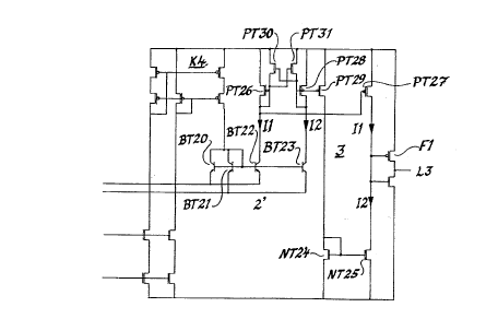
Fig. 5 shows a wiring diagram of a signal-receiving and
signal=processing unit 1 according to Applicant's invention,
where the signal-receiving circuit 2 comprises four NMOS
transistors, NT20, NT21, NT22, NT23 intended for a
pronounced differential signal transmission. w
The transistors NT20, NT21 are supplied with a current
through' a current originating from the cascode circuit K4
comprising PMOS transistors to generate a total current IT
from the sum of the currents II, I2 that pass through the
transistors NT20, NT21. The. current I1 is supposed to pass
through the transistor NT20 and the current I2 is supposed
to pass through the transistor NT21 in dependence on the
momentary voltage differences appearing on the conductors
L1, L2.
The relation between II + I2 and IT is always constant_
The voltages on the conductors L1, L2 are normally
distributed in a way such that either the current I1 or the
current I2 passes, and only during the switching time does a
current pass through both transistors NT20, NT21.
WO 95122853 PCT/SE95/00165
-20-
As voltage pulses appear on the conductors Ll, L2, the
momentary voltage relation that. is received by the signal-
receiving circuit 2, that is detected by its transistors
NT20, NT21, and that generates the corresponding changes in
the momentary currents I1, I2 changes.
Fig. 5 is intended to illustrate that, in accordance with
the invention, the current Il is current-mirror connected
through the transistor NT22 and the current I2 is current-
IO mirror connected through the transistor NT23.
The wiring diagram illustrates that the current I1 is
mirrored in a further current mirror circuit made of
transistors PT26, PT2? before I1 has an effect on the
amplifier Fl. The current I2 is mirrored both in a current
mirror circuit made of transistors PT28, PT29 and in a
current Fnirror circuit made of transistors NT24, NT25 before
it has an effect on the amplifier F1.
The momentary current difference I1-I2 affects the
momentary voltage on the input terminal of the amplifier F1
in the same way as described with reference to Fig. 3.
With differential signal transmission, this circuit provides
a EM area corresponding to that which is specified in Fig.
4, and the limit value of the repetition frequency has
increased to the Gb/s or GHz range to the use of NMOS
transistors and current mirror circuits at least in the
signal-receiving circuit 2.
It should be noticed that NMOS transistors are used in the
upper part of the illustrated wiring diagram and_NMOS
transistors in the lower part.
,. 35 It can, in conclusion, be said that the use of transistors
with a short reaction time, such as NMOS transistors, in the
WO 95/22853 PGTlSE95100165
-2I-
receiver circuit 2 is required to be able to detect the
transition between one information-carrying digital voltage
pulse and another, but it is notyrequired to have such fast
circuits for the following signal processing, once that
S transition is detected.
Differential signal transmission illustrated in Fig. 5 can
be further transformed in a simple way into single-ended
transmission by locking the potential of conductor L2
voltage-wise or by using the simplified wiring diagram shown
in Fig. 5a.
The embodiment illustrated in Fig. 5 indicates that a first
transistor NT20 is connected to a first conductor L1 and
that a second transistor NT21 is connected to a second
conductor L2.
It is further indicated that two transistors NT20, NT22 and
two transistors NT21, NT23, or several transistors, are
respectively connected to one and the same conductor L1, L2.
It is hereby meant that.one..transistor, such as NT20., can
comprise one transistor or several transistors connected in
parallel and that the two or more transistors belonging to a
cu~crent mirror circuit can in this regard differ from one
another.
The transistor NT23 could thus comprise two or several
parallel-connected transistors, while the transistor NT2I
could comprise a single transistor whereby an amplifier
circuit is inserted in between them.
This permits "scaling" the current relations between the
total current IT and the sum of the currents I1 and I2 and
in this manner saving power.
WO 95/22853 PCT/SE95/00165
-22-
Fig. 5 illustrates further that the pair-wise transistors
NT20,. NT22 and NT21,.NT23 for the conductors Ll, L2,
respectively, are connected to each other as a current
mirror circuit each.
The~thereby appearing and received current difference in the
signal-processing circuit 3 can be fed out as ~a pulsed
voltage-related output signal on the conductor L3, having an
internal selected signal structure. The pair-wise
transistors NT20, NT22 and NT21, NT23 from the respective
conductors L1, L2, can be regarded as serving as double
floating current mirror circuits.
There is nothing to prevent each and every one of. the
current mirror circuits, such as the transistors NT24, NT25,
PT28, PT29 and the transistors PT26, PT27, from creating the
conditions -°-for: a - cascode -circuit' or the like ~ and thereby
further improving the internal signal structure of the
output signal appearing on conductor L3.
In the above-described embodiments, the current I1 is
. permitted to be activated by one current mirror circuit
(transistors PT26, PT27) while the current I2 is permitted
to be activated by two current mirror circuits (transistors
PT28, PT29 and transistors NT24, NT25). In principle, this
will produce a time delay of the current pulses from I2 to
the amplifier F1 and a distortion of the switching time for
the amplified and inverted signal on conductor L3.
This distortion can be compensated by giving the two
transistors PT11, NT12 different sizes, thereby changing the
switching level of the amplifier F1. .
The PMOS transistors PT30, PT31 illustrated in Fig. 5 are
" 35 connected to shorten the switching time as the two currents
Il, I2 are switched. The two feedback-connected transistors
W0 95/22853 i PGTISE95100165
-23-
present two loads with a negative impedance, which in turn
helps. to speed up the switching time.
An alternative embodiment to the circuit illustrated in Fig.
5 is illustrated in Fig. 6, which shows-the transistors
NT20, NT20' mutually connected to the conductor L1 and the
transistors NT21, NT21' mutually connected to the conductor
L2.
Also, a cascode circuit is provided at the input stage
(transistors NT20-NT23) that improves the input CM
characteristics. This makes the currents I1, I2 less
dependent on the CM voltage of the input, which in turn
reduces~the time variations in the signal-processing stage
since the sum of the currents is constant. The transistors
NT20', NT21' are for generating the required voltage
reference (Vref) for the cascode circuit. -
The voltage difference between the conductors L1, L2 is
detected by the transistors NT20, NT21 and provides thereby
the required voltage reference for the current transistors
in the cascode circuit (one of them being illustrated as
transistor NT23b).
The voltage difference between the conductors L1, L2 is also
detected by the transistors NT20', NT21' and has thereby an
effect on the cascode transistors in the cascode circuit
(one of them being illustrated as transistor NT23a).
In Fig. 7, a signal-receiving and signal-processing unit 1'
is illustrated in which a signal-receiving circuit 2'
comprises bipolar transistors that are mainly connected in
the way indicated by the wiring diagram in Fig. 5, but where
transistors, such as transistors BT20, BT21, are connected
to respective ones of the conductors L1, L2 by their
respective emitter terminals.
WO 95122853 PGT/SE95I00165
~18Z945
The transistors BT20-BT23 correspond to the transistors
NT20-NT23 in Fig. 5 and are connected in the same way.
The embodiment at large, according to Figs. 5 and 6, can be
applied to Fig. 7.
The now illustrated embodiments have been described with the
understanding that the voltage-related signals appearing on
the conductors L1, L2 are to be evaluated as voltage
differences and converted into current differences (I1-I2).
The above-described circuits will work in the same way for
single-ended signalling, with the difference that one
conductor (for instance, the conductor L2) is given a
constant reference potential (see Figs. 7a and 9).
Fig. 7a-(and Fig.'Sa) illustrates a simplified single-ended-
circuit for single-ended signalling on the conductor L1,
with the transistors BT2la, BT23a forming a current mirror
circuit for keeping the current I2 constant and the
transistor BT22a generating the current variations in the
current I1 corresponding to the voltage variations o_n the .
conductor L1.
In general it can be said that, if NMOS transistors are ,
used, the source terminal is to be connected to the
conductor L1 or L2 having the.lower potential level and the
drain terminal is to be connected to the higher potential.
A CMOS transistor is normally, physically speaking, totally
symmetrical, and thus the question of drain or source
terminal is more a matter of definition. ..
._ 3S It is specifically indicated (in Fig. 5) that the
transistors NT22, NT23 in any case can be doubled, or even
WO 95/22853 PCT/SE95/00165
-25-
consist of more transistors, to thereby create a changed and
_ selected amplification of the reference current IT with the
purpose of saving the total current consumption, which in
the dimensioning instructions also can be relevant for other
illustrated transistor circuits.
Fig. 8 illustrates a wiring diagram with bipolar transistors
BT20, BT21, BT22, BT23 being a part of the signal-receiving
circuit 2~' and with the signal-processing circuit 3
comprising some NMOS transistors and several PMOS
transistors for generating a CMOS-adapted output signal on
the conductor L3.
The PMOS and NMOS transistors in the current mirror circuits
(PT26, PT27, PT28, PT29 and NT24, NT25) are also seen in
Fig. 5.
Variations in the currents I1, I2 will, as described with
reference to Fig. 7, generate a voltage difference across
the resistances RI; R2 that will be amplified by the post-
connected differential stage BT24, BT25, which in turn will
provide a voltage drop across the resistances R3, R4.
The voltage differences across the resistances R3, R4 form
ECL signals on the highest level.
If it is desired to shift the level of the ECL signals down,
this can be achieved with post-connected emitter followers
in a known way.
The transistors BT22, BT23 can each be made of several
parallel-connected transistors, as the respective NMOS
transistors NT22, NT23, for amplifying the reference
current IT.
WO 95122853 PGTISE95/00165
It is further within the scope of Applicant's invention.to
divide one or several of the transistors into parallel-
connected smaller transistors in a known way, thereby
increasing the accuracy.
The'bandwidth or highest rate in the signal-receiving
circuit 2 and/or the signal-processing circuit 3 can be
increased by increasing the reference current IT.
The bandwidth can be selected to correspond to a selected
reference current, and the reference current can be
decreased at lower transmission rates with the result that
power consumption is decreased.
Fig. 9 illustrates a wiring diagram of a compensating
circuit that is specifically adapted to single-ended
signalling and that has~a reference voltage connected to the
conductor L2.
The illustrated compensating circuit is a complement to the
embodiment shown in Fig. 8, but it can also be useful with
the embodiments illustrated in Figs. 5, 6, and 7.
Through two NMOS transistors NT90, NT91, each connected to a
respective one of the conductors L1, L2, the gate terminals
are mutually connected and controlled by a reference current
Iref, which is a current that will represent the total
current IT.
The compensating current IT, passing through both
transistors NT90, NT91, stands in.proportion to Iref and
. thereby also to the current IT + I1 + I2 passing~-~through the
transistors BT20 - BT23 in the signal-receiving circuit 2':
These currents will even each other out, whereby no current
will appear in the conductors L1, L2 when these are in
balance.
WO 95/22853 PGT/sE95/00165
2 ~ 8~~43
~_27-
It will be understood that Applicant's invention is not
restricted to the aforesaid and the illustrated exemplifying
embodiments thereof and that modifications can be made
within the scope of the following claims.