Note: Descriptions are shown in the official language in which they were submitted.
CA 02182974 1999-09-23
1
SYSTEM AND METHOD FOR HIGH SPEED DATA TRANSFER
BACKGROUND
The field of the present invention pertains generally to
data communications equipment, and more particularly to a device
for transmitting digital data over a telephone connection.
Data communication plays an important role in many
aspects of today's society. Banking transactions, facsimiles,
computer networks, remote database access, credit-card validation,
and a plethora of other applications all rely on the ability to
quickly move digital information from one point to another. The
speed of this transmission directly impacts the quality of these
services and, in many cases, applications are infeasible without a
certain critical underlying capacity.
At the lowest levels, most of this digital data traffic
is carried over the telephone system. Computers, facsimile
machines, and other devices frequently communicate with each other
via regular telephone connections or dedicated lines which share
many of the same characteristics. In either case the data must
first be converted into a form compatible with a telephone system
designed primarily for voice transmission. At the receiving end
the telephone signal must be converted back into a data stream.
Both tasks are usually accomplished by modems.
CA 02182974 1999-09-23
2
A modem performs two tasks corresponding to the needs
above: modulation, which converts a data stream into an audio
signal that can be carried by the telephone system, and
demodulation, which takes the audio signal and reconstructs the
data stream. A pair of modems, one at each end of a connection,
allows bidirectional communication between the two points. The
constraints on the audio signal create the limitations on the speed
at which data can be transferred using modems. These constraints
include a limited bandwidth and degradation of data by noise and
crosstalk. The telephone system typically can carry only signals
that range in frequency between 300 Hz and 3.400 Hz. Signals
outside this range are sharply attenuated. This range was built
into the design of the telephone system since it covers a
significant portion of the human voice spectrum. However, the
bandwidth of a channel is one factor that determines the maximum
attainable data rate. With all other factors constant, the data
rate is directly proportional to the bandwidth.
Another factor is the distortion of the audio signal or
any other signal that the communications endpoints cannot control.
This includes electrical pickup of other signals being carried by
the telephone system (crosstalk), electrical noise, and noise
introduced by conversion of the signal from one form to another.
The last type will be expanded upon in later discussion.
CA 02182974 1999-09-23
3
For general utility, modems are designed to be operable
over most telephone connections. Thus, they must be designed for
worst-case scenarios, which include bandwidth limitations and
significant noise that cannot be removed. Even so, substantial
progress has been made on modem design in the past several years.
Devices capable of operating at speeds up to 28,800 bits per second
are now commonly available. See International Telecommunication
Union, Telecommunication Standardization Sector (ITU-T),
Recommendation V.34, Geneva, Switzerland (1994). However,
theoretical arguments based on the channel bandwidth and noise
levels show that the maximum possible speed has nearly been
obtained and further significant increases are highly unlikely with
the given constraints. This is discussed in C.E. Shannon, "A
Mathematical Theory of Communication", Bell System Technical
Journal, 27:379-423, 623-656 (1948).
Unfortunately, although speeds approaching 30,000 bits
per second (or 3,600 bytes per second) make many data
communications applications feasible, conventional modem
transmission is still not fast enough for all uses. At these
speeds, transmission of text is fast, and low-quality audio, such
as digitized speech, is acceptable. However, facsimile or still-
image transmission is slow, while high-quality audio is limited and
full-motion video has not been satisfactorily achieved. In short,
CA 02182974 1999-09-23
3a
what is needed is greater data transmission capability. This is a
prerequisite for the new applications and is a necessity for
maximizing the performance of many existing applications.
Of course, the telephone companies, cable-television
providers, and others are not ignorant of these increasing data
transmission needs. One approach to providing higher speed data
connections to businesses and residences is to provide end-to-end
digital connectivity, eliminating the need for additional modems.
One offering of such a service is the Integrated Services Digital
Network (ISDN). See: International Telecommunication Union,
Telecommunication Standardization Sector (ITU-T), "Integrated
Services Digital Networks (ISDNs)", Recommendation I.120, Geneva,
Switzerland (1993), and John Landwehr, "The Golden Splice:
Beginning a Global Digital Phone NetWOrk", Northwestern University
(1992). ISDN replaces the existing analog local loop with a
160,000 bit/second digital connection. Since the bulk of long-
distance and inter-office traffic is already carried digitally,
this digital local loop can be used for end-to-end digital voice,
computer data or any other type of information transfer. However,
to achieve these data transmission rates on the local loop, special
equipment must be installed at both ends of the line. Indeed, the
entire telephone network is currently undergoing a transformation
CA 02182974 1999-09-23
3b
from a voice transmission network to a general data transmission
service, with voice just being one particular form of data.
Once installed, each basic ISDN link will offer two data
channels capable of 64,000 bits/second, a control channel with a
capacity of 16,000 bits/second, reduced call connection time, and
other benefits. At these rates, facsimile and still image
transmission will be nearly instantaneous, high-quality audio will
be feasible, and remote computer connections will benefit from a
fivefold speed increase. Some progress toward full-motion video
may also be achieved.
~. t~ ~:; i ~:
WO 96!18261 218 2 9 7 4 pCTIUS95115924
-4-
The down side of ISDN is its availability, or lack thereof. To use ISDN, the
user's central office mns~ be upgraded to provide this service, the user must
replace
its on-premises equipment (such as telephones) with their digital equivalents,
and
each individual line interface at the central office must be modified to carry
the
digital data stream. This last step, the conversion to a digital link of the
millions
of analog connections between every telephone and the central office, is
formidable.
The magnitude of this task dictates that the deployment of ISDN will be slow
and
coverage will be sporadic for some time to come. Rural and sparsely populated
areas
may never enjoy these services.
Another existing infrastructure potentially capable of providing high-speed
data
communications services is the cable television system. Unlike the telephone
system,
which connects to users via low-bandwidth, twisted-pair wiring, the cable
system
provides high-bandwidth connectivity to a large fraction of residences. Unused
ca-
pacities on this wiring could provide data rates of tens, or even hundreds, of
millions
of bit per second. This would be more than adequate for all of the services
envi-
sioned above including full-motion digital video. However, the cable system
suffers
from a severe problem-its network architecture. The telephone system provides
point-to-point connectivity. That is, each user has full use of the entire
capacity
of that user's connection-it is not shared with others and does not directly
suffer
due to usage by others. The cable system on the other hand, provides broadcast
connections. The entire capacity is shared by all users since the same signals
appeal
at each user's connection. Thus, although the total capacity is high, it is
divided by
the number of users requiring service. This architecture works well when all
users
require the same data, such as for cable's original design goal, television
distribu-
tion, but it does not serve well a community of users with different data
needs. In a
metropolitan area the data capacity available to each user may be
significantly less
than via an ISDN or modem connection.
To provide high-speed, data connectivity to a large number of users, the cable
system could be modified to isolate different segments of the user population
effec-
CA 02182974 1999-09-23
tively sharing the cable bandwidth over smaller populations.
However, like ISDN, this will be a slow, costly process that will
provide only partial service for many years to come.
The methods used to design modems are based largely on
models of the telephone system that have remained unchanged for
several decades. That is, a modem is modeled as an analog channel
with a finite bandwidth (400-3400 Hz) and an additive noise
component on the order of 30 dB below the signal level. However, a
large portion of the telephone system now uses digital transfer of
a sampled representation of the analog waveforms for inter-office
communications. At each central office, the analog signal is
converted to a 64,000 bit/second pulse code modulated (PCM) signal.
The receiving office then reconstructs the analog signal before
placing it on the subscriber's line. Although the noise introduced
by this procedure is, to a first approximation, similar to that
observed on an analog system, the source of the noise is quite
different. See K. Pahlavan and J.L. Holsinger, "A Model for the
Effects of PCM Compandors on the Performance of High Speed Modems",
Globecom '85, pages 758-762, (1985). Most of the observed noise on
a telephone connection that uses digital switching is due to
quantization by the analog-to-digital converters needed to convert
the analog waveform into a digital representation.
CA 02182974 1999-09-23
6
As noted above, most telephone connections are currently
carried digitally between central offices at rates of 64,000
bits/second. Furthermore, ISDN services demonstrate that it is
possible to transmit significantly more than these rates over the
local loop. It has been suggested that it may be possible to
design a transmission scheme that takes advantage of these factors.
Kalet et al. postulate a system, shown in Figure 2, in which the
transmitting end selects precise analog levels and timing such that
the analog-to-digital conversion that occurs in the transmitter's
central office might be achieved with no quantization error.
I. Kalet, J.E. Mazo, and B.R. Saltzberg, "The Capacity of PCM
Voiceband Channels", IEEE International Conference on
Communications '93, pages 507-511, Geneva, Switzerland (1993). By
making use of the mathematical results of J.E. Mazo it is
conjectured that it should be theoretically possible to reconstruct
the digital samples using only the analog levels available at the
receiver's end of the second local loop in the communications path.
J.E. Mazo, "Faster-Than-Nyquist Signaling", Bell System Technical
Journal, 54:1451-1462 (1975). The resulting system might then be
able to attain data rates of 56,000 to 64,000 bits/second. The
shortcoming of this method is that it is nothing more than a
theoretical possibility that may or may not be realizable. Kalet
et al. State that, "This is a hard practical problem and we can
CA 02182974 1999-09-23
6a
only conjecture if a reasonable solution would be possible." Id. at
page 510.
An example of a conventional attempt to solve the
foregoing problem is found in work by Ohta, described in U.S.
Patent Numbers 5,265,125 and 5,166,955. Ohta disclosed an
apparatus to reconstruct a PCM signal transmitted through a
communications channel or reproduced from a recording medium.
These patents exemplify some conventional techniques abundant in
the literature to deal with the general problem of reconstructing a
multi-valued signal that has passed through a distorting channel.
See also, for example, Richard D. Gitlin, Jeremiah F. Hayes and
Stephen B. Weinstein, "Data Communications Principles", Plenum
(1992). However, such conventional teachings do not consider the
application of methods to handle the output from a nonlinear
quantizer, nor do they deal with the specific problems of decoding
digital data passed over a telephone local loop. Furthermore, the
problem of reconstructing a sampling rate clock from the PCM data
is non-trivial when the PCM signal can take on more than two
values. For example, in the patents by Ohta, a simple clock
recovery scheme which relies on a binary input signal is employed.
This type of clock recovery cannot be used with the multivalued
CA 02182974 1999-09-23
6b
codes used in a telephone system. Also, compensation for drift with
time and changing line conditions requires use of an adaptive
system which the prior art of PCM reconstruction does not include.
,, ,~~ " r.~- 2182974
W0 96/18261 PCTIUS95115924
Thus. there is currently a critical disparity between the required or desired
data
communications capacity and that which is available. Existing modems do not
pro-
~ vide adequate capacities, and new digital connectivity solutions are several
years
away from general availability. Refitting the existing infrastructure with
ISDN ca-
pability is a sizable task and may take a decade before its use is widespread.
A new
method of data transmission could immensely benefit many current applications
as
well as making several new services available which would otherwise have to
wait
until the infrastructure catches up with the requirements.
Accordingly, there is a need for providing a new system of data transfer which
provides the capability to receive data at high raies over existing telephone
lines.
There is also a need for an improved system of data transfer which can enable
systems, equipment, and applications designed for a digital telephone system
(such
as ISDN) to be used with analog connections.
There is also a need for an improved system of data transfer which is capable
of taking advantage of the digital infrastructure of the telephone system
without
requiring costly replacement of all subscribers' lines.
It also would be desirable to create a high speed communication system to pro-
vide a means to distribute high-quality digital audio, music, video, or other
material
to consumers. Such an improved system of data transfer would advantageously
pro-
vide a means to distribute, on-demand, individually-tailored information,
data, or
other digital material to a large number of consumers.
There is also a need for an improved high speed communications system to
provide greater throughput for commercial applications such as facsimile,
point-
of sale systems, remote inventory management, credit-card validation, wide-
area
computer networking, or the like.
2182974
W0 96118261 PCT/US95115924
_g_
SU1~II~iARY
One aspect of the present invention comprises a system for transferring data
over
existing telephone connections at rates higher than known modems or
conventional
methods of data transmission. The present invention achieves a significant
improve-
ment over conventional methods by making use of two critical observations:
I. The underlying phone system is digital using PCM transmission.
2. High data rates are required in one direction only, the source of which has
direct digital access to the telephone system.
An aspect of the present inveniion utilizes the foregoing observations to
achieve
higher data transmission rates than were previously attainable with
conventional
systems. The second observation above addresses the largest use of modems-to
access and retrieve information from centialized servers. In addition, the
present
invention has been found particularly useful for applications that require
higher data
rates, such as database access and video or audio on demand. Such applications
can
be realized, utilizing the high data transmission rates that are attainable
through
the present invention.
An important aspect of the invention is both simple and extremely powerful;
that
is, to allow the data provider to connect directly to a digital telephone
network while
the consumer uses its existing analog connections without change to the line.
This
configuration greatly changes the model under which the consumer's data
equipment
must operate. Existing modems must deal with bandwidth limitations and
multiple
unidentified noise sources that corrupt a signal over the entire transmission
path.
In contrast, an aspect of the present invention carries data digitally over
the bulk
of the path, from the central office to the consumer's home or office, and
converts
it to analog form only for the last segment of that path. Advantageously, one
of
the primary sources of noise to existing modems, quantization noise during
analog-
to-digital conversion, is completely eliminated, since such conversion is no
longer
-, v ,~. r ,~
21829.74
WO 96/18261 PCTlUS95/15924
_g_
required. Furthermore, quantization noise during digital-to-analog conversion.
can
be modeled as a deterministic phenomenon, and thus significantly reduced.
By using the foregoing aspect of the invention, the data source, which has
direct
access to the digital network (for example, by ISDN), can transfer exact data
to
the central office serving the consumer of the data. All that is then required
is a
device at the consumer's end of the local loop that will compensate for
distortion of
the data signal due to the filtering performed at the central office's digital-
to-analog
converters and due to the transmission line. Both distortions can be dealt
with
adequately using existing digital signal processing hardware, as will be
described
herein.
Note that although this method cannot be used for return data from the con-
sumer to the server, existing modems can be used, giving an asymmetrical
channel
with a capacity of up to 64,000 bits/second from server to consumer and 20,000
to
30,000 bits/second return.
It will be appreciated that an aspect of the invention enables digital data of
aay type (audio, video, information, or the like) to be sent to individual
users at
speeds higher than can be obtained with conventional modems, or conventional
methods of data transfer. Flwthermore, unlike cable television distribution
systems,
this invention can service, at the full data rate, any number of users
simultaneously
requesting different data.
Beyond providing greater speed of operation for existing applications, such as
remote computer access, high-speed facsimile transmission, etc., certain
aspects of
the invention make several new applications possible. These include high-
quality
audio or music transmission, video-on-demand, still picture transmission,
video-
phone, teleconferencing, or like applications in which high data transmission
rates
are essential.
Another aspect of the present invention is to reconstruct a multivalued PCM
data signal from an analog representation of that signal. This is achieved
using a
new method which combines a novel clock synchronization technique with
adaptive
CA 02182974 1999-09-23
equalization.
In addition to the foregoing, other aspects and
advantages of the present invention include: (1) the ability to
effectively reconstruct the telephone system's digital pulse-code-
modulated (PCM) data stream using only the analog signal at the
subscriber end of the telephone line; (2) the ability to
reconstruct the clock frequency and phase of the PCM data, using
only the analog signal at the subscriber end of the telephone line;
(3) the ability to increase the effective data rate between a
10 central office and the subscriber end without adding additional
equipment at the central office or otherwise modifying the
telephone system; and (4) the ability to reconstruct said digital
data after such data has been modified due to one or more of
conversion to analog form, filtering, distortion, or corruption by
the addition of noise.
The invention may be summarized, according to one broad
aspect, as a high speed data transfer system for communicating
between a digital data source and an analog subscriber connected to
a digital telephone network by an analog loop comprising: an
encoder coupled to said digital data source, said encoder
converting an input from said data source into a series of
codewords from a set of codewords corresponding to quantizer values
utilized by said digital telephone network; an interface for
CA 02182974 1999-09-23
l0a
transmitting said series of codewords in digital form from said
encoder to said digital telephone network; and a decoder coupled by
said analog loop to said digital telephone network, wherein said
analog loop provides an analog signal to said decoder, which analog
signal is an analog representation of said series of codewords, and
wherein said decoder is responsive to said analog signal to
reconstruct said series of codewords in digital form from said
analog signal.
According to another aspect, the invention provides a
high speed data transfer method for a communications system
connecting a data source to a subscriber, wherein said subscriber
is connected to a digital telephone network by an analog loop and
said data source is connected through a digital connection to said
digital telephone network, said method comprising the steps of:
selecting a subset of digital codewords from a set of digital
telephone network codewords, said digital telephone network
codewords corresponding to a set of quantization values applied at
a line interface which couples said digital telephone network to
said analog loop; mapping a data stream produced by said data
source into a sequence of digital codewords from said subset of
digital codewords; transmitting said sequence of codewords through
said digital connection to said digital telephone network;
converting said sequence of codewords into an analog signal at said
CA 02182974 1999-09-23
lOb
line interface; and at said subscriber, reconstructing said
sequence of codewords from said analog signal.
According to yet another aspect, the invention provides a
method for transferring data between a first party having digital
connectivity to a telephone system and an analog subscriber to said
telephone system comprising the steps of: encoding digital data at
the first party into a sequence of symbols from a set of
quantization symbols corresponding to quantizer values utilized by
said telephone system and utilized at a line interface connecting a
digital portion of said telephone system to said analog subscriber;
transmitting said sequence via said telephone system, said
transmitting step comprising the step of converting said sequence
at said line interface into an analog signal for reception by said
subscriber; and at said analog subscriber, decoding the received
analog signal to recover said digital data.
According to still another aspect, the invention provides
a high speed data transfer system for communicating between a
digital data source and an analog subscriber connected to a digital
telephone network by an analog loop, comprising: an encoder
operatively associated with said digital data source, said encoder
converting an input from said data source into a series of
codewords from a set of codewords associated with quantizer values
determined by said digital telephone network; an interface for
CA 02182974 1999-09-23
10c
transmitting said series of codewords in digital form from said
encoder to said digital telephone network; a digital-to-analog
converter located at a line interface between said digital
telephone network and said analog loop, wherein said converter
provides an analog signal to said subscriber over said analog loop,
which analog signal is a representation of said series of
codewords; and a decoder associated with said subscriber and
connected to said analog loop, said decoder being responsive to
said analog signal provided to said subscriber by said converter to
reconstruct, from said analog signal, said input from said data
source.
DESCRIPTION OF DRAWINGS
These and other features, aspects and advantages of the
present invention will become better understood with regard to the
following descriptions, appended claims and accompanying drawings
in which:
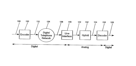
Figure 1 is a block diagram showing a typical modem data
connection;
Figure 2 is a block diagram showing an example of a
hypothetical symmetric digital system;
Figure 3 is a block diagram showing a high speed
distribution system in accordance with an aspect of the present
CA 02182974 1999-09-23
lOd
invention;
Figure 4 is a block diagram of a hardware implementation
of an encoder 150 of Figure 3, in accordance with an aspect of the
present invention;
Figure 5 is a block diagram showing the function of
encoder 150 of Figure 3, in accordance with an aspect of the
present invention;
.. , ~'"~ i ~ 'i4 y ~,
WO 96!18261 2 ~ 8 2 9 ~ 4 PCT/US95/15924
-11-
Figure 6 is a block diagram showing the function of a DC eliminator 184 of
Figure
5, in accordance with an aspect of the present invention;
Figure 7a is a graph of a data stream 100 as a function of time. such as would
be
applied to encoder 150 in accordance with an aspect of the present invention;
Figure 7b is a graph of a typical output from encoder 150 as a function of
time,
such as would be applied to a digital network connection 132 of Figure 3, in
accordance with an aspect of the present invention;
Figure 7c is a graph of a linear value 194 of Figure 6 as a function of time;
this is the output signal from encoder 150 after conversion to linear form, in
accordance with an aspect of the present invention:
Figure 8 is a block diagram showing the function of existing digital line
interfaces,
for reference in understanding an aspect of the present invention;
Figure 9 is a block diagram of a hardware implementation of a decoder 156
shown
in Figure 3, in accordance with an aspect of the present invention;
Figure 10 is a block diagram showing the function of decoder 156 of Figure 3,
in
accordance with an aspect of the present invention;
Figure lla is a graph of an analog signal 154 of Figure 10 as a function of
time,
in accordance with an aspect of the present invention;
Figure lIb is a graph of a compensated signal 274 of Figure 10 as a function
of
time, formed within decoder 158 in accordance with an aspect of the present
invention;
Figure llc is a graph of an estimated code stream 280 of Figure 10 as a
function of
time, formed within decoder 156 in accordance with an aspect of the present
invention;
2182914
t l
WO 96118261 ~ PCTlUS95115924
-12-
Figure lld is a graph of a data stream 126 of Figure 3 as a function of time,
gen- .
crated by decoder 156 in accordance with an aspect of the present invention;
Figure lle is a graph of an error signal 272 of Figure 10 as a function of
time,
generated by decoder 15B in accordance with an aspect of the present inven-
tion;
Figure 12 is a block diagram showing an inverse filter 268 of Figure 10, in
accor-
dance with an aspect of the present invention;
Figure 13 is a block diagram showing a feed-forward equalizer 300 of Figure
12,
in accordance with an aspect of the present invention;
Figure 14 is a block diagram showing a filter tap 330 of Figure 13, in
accordance
with an aspect of the present invention;
Figure 15 is a block diagram showing a clock estimator 264 of Figure 10, in
accordance with an aspect of the present invention;
Figure 1B is a block diagram showing the function of a clock synchronizer 260
of
Figure l0,in accordance with ~n aspect of the present invention;
Figure 17 is a block diagram showing a,n end-to-end asymmetric system with a
reverse channelin accordance with an aspect of the present invention;
Figure 18 is a block diagram showing an application of an aspect of the
present
invention with a database server;
Figure 18 is a black diagram showing an aspect of the present invention in an
application to a high speed facsimile system;
Figure 20 is a block diagram showing a digital telephony relay in accordance
with
an aspect of the present invention.
r,
2182974
WO 96!18261 PCTIUS95/15924
-13-
DESCRIPTION
Conventional Modem Data Connection
A conventional modem data connection is shown in Figure I. Operation of such a
system is well known and has been standardized by government agencies such as
the
International Telecommunications Union. Depending on the types of a modem 104
and a modem 124, data may be applied at rates of up to 28,800 bits/second via
the
first user's data stream 100. Modem 104 converts data stream 100 into an
analog
signal, which is applied to a local loop 106, which in turn connects to a
telephone
switch 108. The analog signal is then carried through a telephone network 114
via
a network connection 112 and eventually reaches, via a network connection 118,
a
telephone switch 120 serving the second user. The signal is then passed, in
analog
form, via a local loop 122 to the second user's modem 124, which converts the
signal to data stream 126, which will be a delayed version of data stream 100.
In
an exactly analogous way, a data stream 128 travels through the telephone
network
via modem 124, local loop 122, telephone switch 120, a network connection 116,
telephone network 114, a network connection 110, telephone switch 108, local
loop
108, and modem 104 to form a delayed version as a data stream 102.
This system assumes that the telephone system reproduces the analog signal,
applied at one user's telephone connection, at the other user's end with
distortion
and delay not greater than a set of standard values specified for the
telephone system.
One can show that, based only on these values, it is not possible to transmit
data
at rates greater than approximately 35,000 bits/second. This system ignores
many
details of the distortion, which may, in fact, be deterministic changes to the
signal
rather than unpredictable changes. One such deterministic change is
quantization
noise if telephone network 114 is implemented digitally. Existing modems
cannot
make use of knowledge of this significant noise source in eliminating
distortion and
are thus limited in their data rates. This is the key shortcoming of existing
modem
systems-low data rate and a theoretical limit on the maximum improvement that
~: :._,. ;; ~ ~~_ 2182974
WO 9G/18261 PCT/US95115924
-14-
will ever be possible within the current framework of assumptions. ,
In an attempt to overcome the foregoing shortcomings and disadvantages of a
conventional modem data connection as shown in Figure 1. an approach to
increas- ,
ing the rate of data transfer has resulted in a hypothetical symmetric digital
com-
munication system. Such a system is shown in combination with a digital
telephone
network in Figure 2.
This system, described by Kalet et al. in the previously cited reference, is
similar
to exisiing modems but with a new assumption: that the underlying
infrastructure
is a digital telephone network 134. The operation is similar to that of the
conven-
tional modem system described above except that the signals are carried in
digital
form within digital telephone network 134 and on a digital network connection
130,
digital network connection 132, a digital network connection 136, and a
digital net-
work connection 138. Each user still requires a modem to transfer the
information
via local loop 122 and local loop lOB to telephone switch 120 and telephone
switch
108 respectively where conversion between analog and a standard digital format
used by digital telephone network 134 is performed.
Unlike conventional modems, no theoretical argument has yet been found which
would limit the speed of such a system to less than that used internally
within
digital telephone network 134, typically 56,000 or 64,000 bits/second. Thus,
it
is hypothetically possible that such a system could obtain data rates up to
64,000
bits/second. However; such a system has never been reduced to practice nor is
there
any evidence that it would be possible to implement such a system. The authors
of
this system state that "This is a hard practical problem and we can only
conjecture
if a reasonable solution would be possible."
The problem is that to make use of the knowledge that the underlying network
is
digital and a large part of the observed signal distortion is due to
quantization noise,
the transmitting modem must control, via only its analog output, the digital
levels
chosen by the network to encode the signal. Furthermore, the receiving modem
must, via only its analog input, accurately infer those digital levels.
Distortion
r~ l i'~~_; f ~ 2182974
WO 96118261 PCT/US95/15924
-15-
due to analog/digital conversion occurs at both the transmitter and receiver's
end
yet only the combined distortion added to the desired signalis directly
observable.
a Furthermore, additional distortion due to electrical noise and crosstalk
also occurs
on local loop 122 and local loop 106. Separating out these distortion
components
from the desired signal and each other is a difficult, perhaps impossible,
task.
One aspect of the present invention is a method by which the shortcomings of
this approach are eliminated. It makes use of knowledge of the underlying
digital
network in a way that is realizable, providing higher attainable data rates
than
possible with any other known solution.
Sampling Rate Conversion
As will be seen in subsequent discussion, a system for recovering PCM data
from
a distorted analog representation requires a method of synchronizing the
decoding
clock with that used to convert the PCM data from a digital stream to analog
values. Digital implementations of this synchronization require that a digital
data
sequence be resampled, changing its rate From that used by an analog-to-
digital con-
verter to one which is closer to that used in conversion from PCM data.
Previously
known techniques for achieving this are either strictly limited in their
capabilities, or
are computationally intensive. See, for example, R.E. Crochiere and L.R.
Rabiner,
"Mullirate Digital Signal Processing," Prentice-Hall, Englewood Cli$'s, NJ,
1983,
which is hereby incorporated herein by reference. Performing sampling rate
conver-
sion between two independent clocks whose relationship may change as a
function
of time further complicates the task.
One aspect of the present invention is a method which can perform such conver-
sion with a minimum of computational overhead. It accepts a continuously-
variable
input/output sampling rate ratio and performs the conversion with high
accuracy.
The techniques described can obtain greater than 90dB anti-aliasing rejection
and
can be implemented in real-time on existing processors.
.,"v s ~. 2182974
WO 96118261 PCTIU595115924
-16-
Overall System
Figure 3 shows an overview of the proposed system. The method of use of the
system
shown in Figure 3 is identical to that for current data communications
circuits or
modems. Data applied at data stream 100 will appear some time later at data
stream 126. Data stream 100 to applied to encoder 150 whose function is to
convert
the data stream into a format compatible with the telephone system. The
converted
data is applied to digital telephone network 134 via digital network
connection 132.
The converted data emerges verbatim via digital network connection 138 at a
client's
telephone central office where a line interface 140 is located. At this point,
if the
client also had direct digital access to the digital connection to the
client's line
interface from digital network connection 138, the transmission would be
complete.
However, where the client, like the majority of users, does not have direct
digital
access to the telephone network, this is not possible, and the following
additional
operations are required.
Line interface 140 converts the digital data on digital network connection 138
into an analog form in a manner conforming to the standardized specifications
of dig-
ital telephony. The analog form is carried on local loop 122 to the client's
premises
where a hybrid network 152 terminates the line and produces analog signal 154.
Hybrid network 152 is a standard part which converts the two-wire
bidirectionaI
signal to a pair of one-way signals. Decoder 156 uses analog signal 154 to
estimate
and compensate for the distortion introduced by the conversion to analog farm
per-
formed by line interface 140, resulting in an estimate of the digital data at
digital
network connection 138, which is assumed to be identical to the digital data
that
was applied at digital network connection 132. The transformation performed by
encoder 150 is then inverted and decoder 156 outputs data stream 126, which is
a
delayed estimate of the original data stream 100.
Note that within Figure 3, all elements are well known and exist within
current
digital telephone systems except encoder 150 and decoder 15B, which will be de-
,; ~:~, ;.~. 2182974
W0 96/18261 PCTIUS95/15924
-17-
scribed in detail below. Also to be described below. is a method of
initializing and
adapting decoder 156 to the exact conditions encountered in normal operation.
Physical Implementation of Encoder
Figure 4 shows a block diagram of one possible realization of encoder 150 of
Figure
3. Data stream 100 from Figure 3 is applied to the serial data input of a
digital
signal processor 160 such as an AT&T DSP32C. This processor uses a processor
bus
162 to communicate with a read-only memory 168. a random access memory 166,
and an ISDN interface circuit 164 such as an Advanced Micro Devices Am79C30A.
Read-only memory 168 contains a stored-program whose functional
characteristics
will be described in following seciions. Random access memory 166 is used for
program storage and parameters. ISDN interface circuit 164 also has an ISDN
connection 170, which is connected to a network terminator 172, such as
Northern
Telecom NTl, and subsequently to digital network connection 132, which was
also
shown in Figure 3.
To produce a fully-functional implementation, additional secondary elements
such as decoders, oscillators, and glue logic would need to be added to the
basic
block diagram shown in Figure 4. Such additions are well known and will be
evident
to those skilled in the art.
Subsequent discussion of encoder 150 will refer to functional rather than
physi-
cal components, all of which can, for example, be implemented as programs or
sub-
routines for digital signal processor 160 using well-known digital signal-
processing
techniques.
Encoder Operation
Figure 5 shows a functional block diagram of encoder 150 of Figure 3. The
channel
from server to client begins with arbitrary digital data provided as data
stream 100.
Encoder 150 converts this bitstream into a sequence of eight-bit words
sampled,
,, ;,.;, ~;:, 21$2974
W0 96118261 PCTIUS95115924
-18-
preferably, at the telephone system's clock rate of 8.000 samples/second. This
is
achieved by a sequence of operations beginning with a serial-to-parallel
converter
180, which groups together each eight bits read from data stream 100,
outputting
a stream of parallel eight-bit values as an 8-bit code stream 182. This
mapping
may preferably be performed such that the first of each eight bits read from
data
stream 100 is placed in the least-significant bit position of 8-bit code
stream 182
with subsequent bits occupying consecutively more significant bit positions
until
the output word is complete, at which point the process repeats. DC eliminator
184 then inserts additional eight-bit values at regular intervals, preferably
once per
eight samples. such that the analog value associated with the inserted value
is the
negaiive of the sum of all prior values on 8-bit code stream 182. This is
necessary
since telephone systems frequently attenuate or remove any DC bias on a
signal.
DC eliminator 184 is one example of a circuit means for reducing DC components
in the received analog signal.
A detail of the functional elements of DC eliminator 184 of Figure 5 is shown
in
Figure 6. A code stream 188 output from a two-input selector 190 is also
converted
to linear value 194 by a ~-law-to-linear converter 192, which can be
implemented
as a 256-element lookup table using the standard p-law-to-linear conversion
table.
Values of linear value 194 are accumulated and negated by a summer 196 and a
unit delay 200 to form a DC offset 198 and a previous DC offset 202, which is
the corresponding unit-delayed value. DC offset 198 is applied to a linear-to-
p-law
converter 204, which can use the same lookup table as p-law-to-linear
converter
192, but performing the inverse mapping. Note that if DC offset 198 is greater
than or less than the maximum or minimum value in the table, the respectively
largest or smallest entry will be used. A DC restoration code 206 is produced
by
linear-to-p-law converter 204 and applied as one input to two-input selector
190.
Two-input selector 190 operates by reading, preferably seven, sequential
values from
8-bit code stream 182 and outputting these values as code stream 188. followed
by
reading and outputting a single value from DC restoration code 206. It then
repeats
~; ,. ~.: y r..~ 2 i 8 2 ° l 4
WO 96!18261 PCTIITS95115924
-19-
this sequence of operations continually. .
Returning to Figure 5, code stream 186 is applied to the input lead of an
ISDN converter 188, which provides the well-known conversion to an ISDN
signal.
The function of ISDN converter I88 is implemented directly by several existing
integrated circuits, including an Advanced Micro Devices Am79C30. The output
of
ISDN converter 188 forms digital network connection 132, which is also the
output
of encoder 150 of Figure 3.
For further understanding, some of the signals used by encoder 150 are illus-
trated in Figures 7a through 7c. Figure 7a shows a sequence of samples of data
stream 100. After processing by serial-to-parallel converter 180 and DC
eliminator
184. code stream 186 is shown in Figure 7b. Within DC eliminator 184, the
linear
equivalent of code stream 186, namely linear value 194, is shown in Figure 7c.
Line Interface
For reference during subsequent descriptions, Figure 8 shows a functional
model of
line interface 140 of Figure 3, such as would be found in a typical telephone
sys-
tem for use with an aspect of the present invention. Note that such interfaces
are
well known and are currently used in digital telephone switches. Digital
telephone
network 134 of Figure 3 passes an eight-bit-per-sample, ~C-law-encoded,
digital data-
stream via digital network connection 138 to a ~-law-to-linear converter 210,
shown
in Figure 8. p-law-to-linear converter 210 implements the well-known IC-law-to-
linear conversion, converting each sample to a linear value 212. Linear value
212 is
then converted to an analog signal 21B by a digital-to-analog converter 214
that is
sampled using a telephone system clock 236 in a well known manner. Although
not
shown in Figure 3 for reasons of clarity, telephone system clock 236 is
generated by
digital telephone network 134. Analog signal 216 is then smoothed by a lowpass
filter 218 to form a filtered signal 220. The main purpose of lowpass filter
218 is
to provide a low-pass function with a cutoff frequency of approximately 3100
Hz.
The International Telecommunications Union has standardized the specifications
for
~~'~'~' ' ~ 2182974
R'O 96118261 PCTIU595115924
-20-
digital-to-analog converter 214 and lowpass filter 218 in International
Telecommu-
nication Union, Telecommunication Standardization Sector (ITU-T),
"Transmission
Performance Characteristics of Pulse Code Alodutation," Recommendation 6.712,
Geneva. Switzerland. September 1992, which is hereby incorporated by
reference.
Filtered signal 220 is multiplexed onto local loop 122 by a four-to-two-wire
converter 222. Local Iqop 122 is bidirectional: incoming signals on local loop
122
are applied to four-to-two-wire converter 222 and are output as an unfiltered
signal
234. Unfiltered signal 234 is applied to a bandpass filter 232, which has also
been
standardized by ITU-T in the above cited reference. The output from ba,ndpass
filter
232, a filtered signal 230, is converted to a linear value 22B by an analog-to-
digital
converter 228. Linear value 226 is then converted to digital network
connection 136
by a linear-to-~-law converter 224, which implements the standard linear-to--
law
conversion. Note that in the system shown in Figure 3, digital network
connection
13B is not used and has been omitted for clarity.
Physical Implementation of Decoder
Figure 9 shows a block diagram of one possible realization of decoder 158 of
Figure
3. Analog signal 154 from Figure 3 is sampled by an analog-to-digital
converter
240, which exists as an integrated circuit, such as a Crystal Semiconductor
CS5016.
This uses a clock signal 244, preferably at 16 kHz, generated by an oscillator
242,
to form a digital input signal 248, which is connected to a bank of digital
signal
processors 245, such as AT&T DSP32C's, via one of their serial digital input
leads.
The processors are also connected to each other and to a random access memory
254 and a read-only memory 252 via a processor bus 250. Read-only memory
252 contains a stored-program whose functional characteristics will be
described in
following sections. Bank of digital signal processors 248 produces data stream
126,
which is the final output of decoder 156 of Figure 3.
To produce a fully-functional implementation, additional secondary elements
such as decoders, oscillators, and glue logic would need to be added to the
basic
C n t~' ~ 1'.
WO 96/18261 2 1 8 2 9 7 4 pCT/US95115924
-21-
block diagram shown in Figure 9. Such additions are well known and will be
evident
to those skilled in the art.
Subsequent discussion of decoder 156 will refer to functional rather than phys-
ical components, all of which can, for example, be implemented as programs or
subroutines for the bank of digital signal processors 248 using well-known
digital
signal-processing techniques.
Decoder Operation
Figure 10 shows the functional structure of decoder 156 of Figure 3. Analog
signal
154 from Figure 3 provides the input data to decoder 156. Analog signal 154 is
fed to analog-to-digital converter 240 and converted to digital input signal
246,
preferably sampled at 16,000 samples per second with 16 bits per sample
precision.
Analog-to-digital converter 240 exists as an integrated circuit, such as a
Crystal
Semiconductor CS5016. Digital input signal 246 is then processed by clock syn-
chronizer 280 which interpolates and resamples digital input signal 248 at
intervals
separated by a period estimate 262 to produce a synchronized signal 286. The
operation of clock synchronizer 280 will be detailed in following sections.
Synchro-
nized signal 288 is filtered by inverse filter 268, which will be described
below, to
reconstruct compensated signal 274. The purpose of inverse filter 268 is to
invert
the transformation performed by line interface 140 of Figure S of which the
primary
component is lowpass filter 218 of Figure 8. Returning to Figure 10, inverse
filter
268 also outputs a delay error estimate 270 giving the timing error inherent
in syn-
chronized signal 28B, which will be used by clock estimator 2B4, described
below,
to compute the period estimate 262 used by clock synchronizer 280. A decision
means is then used to convert compensated signal 274 to a sequence of values
from
a discrete set. As an example, compensated signal 274 is converted to the
nearest
equivalent eight-bit ~-law word using a linear-to-p-law converter 276 to give
esti-
mated code stream 280. As described earlier, linear-to--law converter 276 may
be
implemented as a simple lookup table.
,.;, i ~ 2182974
WO 96118261 PCT/US95/15924
During normal operation. a switch 292 gates estimated code stream 280 back as
a desired output signal 286, which is converted back to a linear signal by a ~-
law-to-
linear converter 278 to form a linear value 284. p-law-to-linear converter 278
can ,
be implemented as a simple lookup table as earlier described. During
initialization,
switch 292 will be set such that apredetermined training pattern 288 (not
shown
in Figure 3) is gated to desired output signal 286. This usage will be
described
below.
Linear value 284 provides an estimate of the desired value of compensated
signal
274. It is used to adaptively update inverse filter 268 such that compensated
signal
274 is as close as possible to linear value 284. This adaptation is one
example of a
training means for adjusting the parameters of decoder 156, which will be
further
explained in the discussion of inverse filter 268 below. A subtracter 282
computes
error signal 272 using compensated signal 274 and linear value 284. Error
signal
272 is fed back to an input lead of inverse filter 288 in a feedback loop.
Estimated
code stream 280 is also passed through a data extractor 290, which inverts the
transformations performed by encoder 150 of Figure 3, to form the decoder's
final
output data stream 128.
For purposes of understanding only, examples of same of the signals present in
Figure 10 are plotted in Figures lla through lle. Figure lIa shows a typical
input
analog signal 154 to decoder 156, as a function of time. During processing of
this
signal, decoder 158 forms compensated signal 274, which is illustrated in
Figure
llb. This signal is further processed to form estimated code stream 280, shown
in Figure lle. Finally, data extractor 290 of Figure 10 outputs data stream
126
shown in Figure lld. Error signal 272, formed for internal use within decoder
158,
is shown in Figure lle.
As mentioned above, analog-to-digital converter 240, subtracter 282, linear-to-
p-law converter 276, switch 292, and ~e-law-to-linear converter 278, all of
Figure
10, are well known and may be easily implemented by anyone skilled in the art.
Following discussion will expand upon the implementation and operation of the
s: r:..,r).i (,
3 , 2182974
W0 96118261 PCTlLTS95115924
-23-
. remaining blocks; inverse filter 288, clock estimator 264, clock
synchronizer 280,
and data extractor 290.
Inverse Filter
Figure 12 shows the internal details of inverse filter 288 of Figure 10.
Inverse filter
288 is an example of an equalization means, which operates by performing
linear
filtering operations on an input signal (synchronized signal 286), to produce
an
output signal (compensated signal 274). Inverse filter 268 also receives error
signal
272 that indicates the mismatch between compensated signal 274 and a desired
value. It uses error signal 272 to update its filtering function such that
error signal
272 in minimized. Such adaptive filter structures are well known; See for
example
Richard D. Gitlin, Jeremiah F. Hayes and Stephen B. Weinstein, "Data Commu-
nicaEions Principles," Plenum (1992), incorporated herein by reference.
However,
far purposes of clarification we will describe herein a preferred
implementation of
inverse filter 288. In addition, inverse filter 288 forms delay error estimate
270,
which is used by clock estimator 284 of Figure 10.
Synchronized signal 28B is fed to feed-forward equalizer 300, which produces
a partially-compensated signal 302 while using a correction signal 324 to
perform
adaptive updates. The operation of feed-forward equalizer 300 will be
described
below. Feed-forward equalizer 300 also outputs delay error estimate 270, which
will be used by clock estimator 284 of Figure 10. Partially-compensated signal
302
is subsequently down-sampled by a factor of two by a downsampler 304 to form
a downsampled signal 30B. Downsampler 304 operates by repeatedly reading two
consecutive values from its input lead and placing the first of these on its
output
lead, discarding the second value. Downsampled signal 306 is then applied to a
subtracter 308 to form compensated signal 274. Compensated signal 274 is used
by subsequent stages in Figure 10 and is also fed into a unit delay 310 to
form a
delayed signal 312. Delayed signal 312 is then applied to the input lead of a
feed-
back equalizer 314 to form a distortion estimate 318. Feed-back equalizer 314
is
, ,~ ,;; r, r ;;
WO 96/18261 PCT/US95115924
-24-
similar to feed-forward equalizer 300 and will be further described below.
Distortion
estimate 316 provides the second input to subtracter 308.
Error signal 272 of Figure 10 is scaled by a constant factor at a gain element
_
318 of Figure 12 to form a correction signal 320. which is applied as a second
input signal to feed-back equalizer 314. Feed-back equalizer 314 uses
correction
signal 320 to perform adaptive updates. Error signal 272 is also up-sampled by
a factor of two by an upsampler 326, which inserts a zero between each sample
of
error signal 272. Upsampler 328 produces an up-sampled error signal 328, which
is
subsequently scaled by a gain element 322 to provide correction signal 324.
The use
of correction signal 320 and correction signal 324 by feed-back equalizer 314
and
feed-forward equalizer 300 respectively will be described below. The values of
the
parameters kf and kb of gain element 322 and gain element 318 respectively
may,
preferably, be in the range 10-a to 10-ls. Optimal values may easily be
obtained
by those skilled in the art without undue experimentation.
Feed-forward and Feed-back Equalizers
Figure 13 shows the internal structure of feed-forward equalizer 300 of Figure
12.
Feed-forward equalizer 300 is composed of, preferably 8 - 128, identical
copies of
filter tap 330 connected in a chain. Any convenient number of tap can be imple-
mented. The first filter tap 330 accepts synchronized signal 2B8 of Figure 12
and
the last filter tap 330 outputs partially-compensated signal 302 used in
Figure 12.
Each intermediate tap takes two input signals: a primary input 332 and a
target
input 336, to form two output signals: a primary output 334 and a target
output
338. Each filter tap 330 also provides, as an output signal, a tap weight 340,
which
is used by a delay estimator 342 to compute delay error estimate 270. During
op-
eration, each filter tap 330 performs adaptive updates using, as an input,
correction
signal 324.
Figure 14 shows the details of the function of each filter tap 330 of Figure
13.
Each tap has two inputs, primary input 332 and target input 336, and provides
=-a~~~~~;~ 2182974
W0 96118261 PCTIITS95/15924
-25-
two outputs, primary output 334 and target output 338, using standard signal
processing blocks as shown in Figure 14. Primary input 332 is delayed by one
sample by a unit delay 350 to form primary output 334. Meanwhile, primary
input
332 is also multiplied by tap weight 340 using a multiplier 352 to give a
weighted
input 354. Weighted input 354 is added to target input 336 by a summer 356 to
give target output 338.
Adaptive update of tap weight 340 is performed by multiplying correction
signal
324 by primary input 332 using a multiplier 366. A multiplier output value 364
provides a tap error estimate and is subtracted from a previous value 360 to
form
tap weight 340 using a subtracter 362. Previous value 360 is formed by a unit
delay
358 using tap weight 340 as input. Each filter tap 330 also outputs tap weight
340.
Returning to Figure 13, each filter tap 330 is fed to delay estimator 342.
Delay
estimator 342 calculates delay error estimate 270 of the overall filter using
the
equation:
i=N
~_~i=lZ~~i__N _.
i=N
~.i=1 ~i 2
where mi is an abbreviation for the i - th tap weight 340. In this way~, delay
estimator 342 provides an estimation means for determining a degree of error
in
period estimate 262 of Figure 10.
The above description of feed-forward equalizer 300 of Figure 10 also applies
to feed-back equalizer 314. The structure and operation of feed-back equalizer
314
are identical to that of feed-forward equalizer 300 with the exception that
delay
estimator 342 is not needed, so there is no equivalent to the delay error
estimate
2T0 output. Also, feed-back equalizer 314 may use a different number of taps
than feed-forward equalizer 300, preferably between one-quarter and on~half
the
number. The optimal number of taps to use for both feed-forward equalizer 300
and feed-back equalizer 314 can be easily obtained by one skilled in the art
without
undue experimentation.
~i8~q74
WO 96118261 PCTIUS95115924
-26-
Clock Estimator ,
Figure 15 shows the functional components of clock estimator 264 of Figure 10.
Clock estimator 264 is one example of a circuit means that uses delay error
estimate
270 to update period estimate 262. The signal input to clock estimator 264,
delay
error estimate 270, is scaled by a factor of kl, preferably in the range 10-~
to 10-s,
but dependent on the accuracy of the clock used for analog-to-digital
converter 240,
by a loop gain 370 to form phase error 374. Phase error 374 is then filtered
with
loop filter 376 to form period offset 378. Loop filter 376 is a low-pass
filter whose
design will be evident to those skilled in the design of phase-locked loops.
Period
offset 378 is added to nominal period 380 by summer 372 to create period
estimate
262. Nominal period 380 is the a priori estimate of the ratio of half of the
sampling
rate of analog-to-digital converter 240 of Figure 10 to the frequency of
telephone
system clock 238 of Figure 8. Since telephone system clock 236 and the clock
used
by analog-to-digital converter 240 are not derived from a common source, the
exact
ratio will differ very slightly from 1.0 for the preferred choices of
parameters. During
operation, period estimate 262 will refine and track this ratio using
estimates of the
current error provided by inverse filter 288 of Figure 10.
Clock Synchronizer
A functional block diagram of clock synchronizer 260 of Figure 10 is shown in
Figure 16. The function of clock synchronizer 260 is to interpolate and
resample
its input signal (digital input signal 246) at intervals separated by period
estimate
262. For example, if period estimate 262 had a value of 2.0, every second
sample
read from digital input signal 24B would be output as synchronized signal 266.
If
period estimate 262 is not an integer, then clock synchronizer 260 will be
required
to appropriately interpolate between input samples to form the output samples.
Clock synchronizer 280 performs one cycle of operation for each output sample
required. Each cycle begins with an accumulator 424 reading the value of
period
v ~ ~ j ~. ~., ~~a~ 218 2 9 7 4
WO 96118261 PCT/US95115924
_27_
estimate 262 of Figure I0. Accumulator 424 forms a running sum of all inputs
values read and outputs this sum as a real-valued sample index 426. This is
scaled
by a factor of Nu, preferably in the range of 10-400, using a gain element 428
to
form an upsampled sample index 430. The optimal value of N" can easily be ob-
tained by one skilled in the art without undue experimentation. An
integer/fraction
sputter 432 decomposes upsampled sample index 430 into a sample index 422 and
a fractional value 414. For example. if upsampled sample index 430 had a value
of
10.7, integer/fraction splitter 432 would set sample index 422 to 10.0 and
fractional
value 414 to 0.7.
One of the input signals applied to a sample selector 398 is formed by a
string of
operations starting with digital input signal 246. An upsampler 390 reads a
value
from digital input signal 246 and outputs N" samples consisting of the value
read
from digital input signal 246 followed by Nu - 1 zero values. The output
stream
from upsampler 390, an upsampled input signal 392, is applied to a low-pass
filter
394, which has a passba.nd cutoff frequency equivalent to 4 kHz. The design of
upsampler 390 and low-pass filter 394 are well known. See, for example, R.E.
Crochiere and L.R. Rabiner, "Multirate Digital Signal Processing," Prentice-
Hall,
Englewood Cliffs, NJ, 1983, which is hereby incorporated herein by reference.
Low-
pass filter 394 forms a filtered upsampled signal 39B, which is used as an
input to
sample selector 398.
Sample selector 398 is an example of a selection means, which reads a value
from sample index 422 and interprets this as a sample number, s". It also
maintains
an internal count of how many samples it has read from its input lead
connected
to filtered upsa.mpled signal 396 since the system was initialized. It then
reads
additional samples from filtered upsampled signal 396 and forms output samples
such that a sample 400 is a copy of sample sn read from filtered upsampled
signal
396 and a sample 402 is a copy of sample s"+i.
Sample 400 is then scaled by fractional value 414 using a multiplier 404 to
form a sample component 408. Similarly, sample 402 is scaled by a fractional
value
:',..f' ;. Y \~
'., ; . .. ~ _. 2182974
W0 96118261 PCTIUS95115924
_28-
416 using a multiplier 406 to form a sample component 410. The magnitude of
fractional value 416 is one minus the magnitude of fractional value 414, as
computed
using a subtracter 420, and a unit constant 418. Sample component 408 and
sample -
component 410 are then added by a summer 412 to form synchronized signal 266,
which is also the output of clock synchronizer 260 of Figure 10. The
combination of
multiplier 404, multiplier 406, and summer 412 is an example of an
interpolation
means for combining the samples selected by sample selector 398.
Clock synchronizer 260 can also be used in other applications or as a
standalone
sampling-rate converter. In general, synchronized signal 266 is equivalent to
digital
input signal 246 but with a different sampling rate. The ratio of the two
rates is
specified by period estimate 262 which may change as a function of time.
Note also that although the linear interpolation may appear to be a coarse
approximation to the desired result, it is in fact quite accurate. By virtue
of the
oversampling performed by upsampler 390, filtered upsampled signal 398 has a
frequency spectra that is near zero everywhere except for a narrow band around
DC.
The interpolation operation effectively creates images of this narrow passband
in the
frequency domain. The function of the linear interpolation is then to filter
out these
images. Conventional implementations use a sharp, computationally-expensive,
low-
pass filter to achieve this. Although the linear interpolator is a very poor
low-pass
filter, it does have very deep spectral notches at exactly the frequencies
where the
undesired images will appeal. It is the combination of the placement of these
notches
with the narrow alias images that makes this method very accurate while
eliminating
much of the computation from traditional techniques.
Data Extractor
The last stage of decoder 156 of Figure 3 is data extractor 290 of Figure 10.
The
function of data extractor 290 is to invert the transformations performed by
encoder
150 of Figure 3. These transformations consist of serial-to-parallel converter
180
and DC eliminator 184 shown in Figure 5.
2182974
v. ~ ' . i Y'.
WO 96118261 PCT/US95/15924
-29-
To invert these transformations, data extractor 290 first removes the values
in-
serted into the data stream by DC eliminator 184. This is done by simply
discarding
every eighth sample read from the input (assuming the DC elimination was done
by
DC eliminator 184 using the preferred rate of once per eight samples). Once
this is
done, the stream of eight-bit values remaining can be converted back into a
serial
data stream 126 by outputting one bit of each word at a time, starting with
the
least-significant bit. Such techniques are well known by those skilled in the
art.
Initialization of System
When a connection is first established between a server and a client, both
encoder
150 and decoder 156 of Figure 3 must commence in a state known to each other.
Within encoder 150 the following initialization is performed:
1. DC eliminator 184 of Figure 5 is initialized with two-input selector 190 of
Figure 8 set such that its next output will be a copy of DC restoration code
206.
2. The output of unit delay 200 of Figure 6, previous DC offset 202, is
initialized
to 0Ø
3. Code stream 186 of Figure 5 is temporarily disconnected from DC eliminator
184. Instead a known sequence of N~, preferably 16-128, values is repeated
Nt, preferably 100-5000, times. The optimal values to use for N~ and N~ can
be easily obtained by one skilled in the art without undue experimentation.
The choice of N~ above is tied to the design of decoder 156. 'N~ is preferably
one-half of the number of taps in feed-forward equalizer 300 of Figure 12.
Without
loss of generality, one possible choice of the sequence of code values
repeatedly
transmitted by encoder 150 is shown in Table 1. An identical sequence is
adsoused
by encoder 150, applied as training pattern 288 in Figure 10.
. ., ;° c. r :-
~. ,
WO 96!18261 218 ~ 9 7 4 pCTIUS95115924
-30-
Table :
1 Typical
Training
Pattern
1.1182 29 140 20 138 153 16
132205 157170 -1 162 129 12
-
8 144 54 134 10 128 G 34
13642 77 25 1481 142 0
Once the N~ repetitions of the sequence have been output, code stream 186 will
be reconnected to DC eliminator 184 and subsequent output from decoder 156
will
correspond to the input applied as data stream 100 of Figure 3.
Within decoder 156 of Figure 3. the following initialization is performed
before
the first sample is read from analog signal 154:
1. Switch 292 of Figure 10 is set to gate training pattern 288 to desired
output
signal 286.
2. Data extractor 290 of Figure 10 is set so the next input value, estimated
code
stream 280, will be considered a DC equalization value and thus be discarded.
3. Unit delay 310 of Figure 12 is initialized to output zero as delayed signal
312.
4. Upsampler 32B of Figure 12 is initialized such that its next output, up
sampled error signal 328, will be a copy of error signal 272.
5. Downsampler 304 of Figure 12 is initialized such that its next input value,
partially-compensated signal 302, will be copied out as downsampled signal
30B.
6. Within feed-back equalizer 314 and feed-forward equalizer 300 of Figure 12,
each unit delay 350 of Figure 14 is initialized to have a zero output.
7. Within feed-back equalizer 314 of Figure 12, each unit delay 358 of Figure
14 is initialized to zero.
v' ; ~~'a' ~ '~ 2l 82974
W0 96/18261 PCT/US95l15924
-31-
8. Within feed-forward equalizer 300, each unit delay 358 of Figure 14 is ini-
tialized to zero.
9. Accumulator 424 of Figure 16 is initialized to output a value of zero as
real-
valued sample index 426.
10. Low-pass filter 394 is initialized with an all-zero internal state.
11. Upsampler 390 is initialized such that its next output. upsampled input
signal
392, will be the value of digital input signal 246.
Decoder 156 then operates as described earlier until N~ ~ Nt values have been
formed at estimated code stream 280 of Figure 10. At this point, switch 292 is
moved to gate estimated code stream 280 to desired output signal 286. From
this
point on, data stream 126 should correspond to data read from data stream 128
as
shown in Figure 3.
It must also be ensured that encoder 150 and decoder 156 enter and leave
initialization mode such that the values on data stream 100 and data stream
126
of Figure 3 are in exact correspondence. One example of a method to achieve
this synchronization is to violate the DC restoration performed by DC
eliminator
184. To signal the beginning of training, code stream 186 is set to the
maximum
legal code value for longer than the normal DG restoration period, for example
for
16 samples. This is followed by setting code stream 186 to the minimum legal
code value for the same number of samples. The training pattern then follows
this synchronization pattern. Similarly, the end of training ca.n be signaled
by
reversing the order of the above synchronization pattern-repeating the minimum
value followed by the maximum value. These synchronization patterns can then
be
detected by decoder 156 and used to control switch 292.
Other techniques for such synchronization are well known and are used in
existing
modems. See, for example, ITU-T, V.34, previously cited.
- . :~-t, f t 2182914
.;., .
WO 96118261 PCTIUS95/15924
-32-
Alternate Delay Estimator
In previous discussion, delay estimator 342 was formed by examination of the
filter
tap weights within feed-forward equalizer 300. Other delay estimation means
are
also possible. For example, error signal 272 and compensated signal 274 of
Figure
can be used to form delay error estimate 270 as follows:
_ a
+k
where D is delay error estimate 270, v is compensated signal 274, a is error
signal
272, and k is a parameter which can be easily obtained by those skilled in the
art
without undue experimentation. The value of k will depend upon the the
relative
contributions of signal noise and clock fitter observed. Any other methods of
im-
plementing a delay estimation means to form delay error estimate 270 may also
be
used in the present invention.
Alternate Decoder Initialization Method
As described above, the parameters of decoder 156 may be established using
fixed
initialization values followed by a training period during which a known data
se-
quence is transmitted. The previously described method uses the training
sequence
to perform sequential updates of the parameters of inverse filter 208 and
clock
estimator 264 on a sample-by-sample basis.
It is also possible to perform a single block update of all parameters. During
the transmission of the training sequence, decoder I58 merely stores the
values
that appear as digital input signal 246. Once the entire traaning sequence has
been transmitted, decoder 158 can perform an analysis of the acquired values
and
calculate values for its internal parameters.
The calculations needed to perform the parameter estimation are as follows:
1. Calculate the fundamental digital period, Tu, of the acquired signal using
a rate estimation means. This can be done using any of a variety of well
2182974
WO 96118261 PCT/US95115924
-33-
known signal processing techniques, such as an autocorrelation analysis. It is
known in advance that Tu is approximately twice N~. the length of the training
. sequence, assuming the use of the preferred sampling rate for analog-to-
digital
converter 240. The only source of difference will be due to differences
between
the sampling rate of telephone system clock 236 and half the sampling rate
of analog-to-digital converter 240.
2. Initialize nominal period 380 of Figure 15 as z~.
3. Resample digital input signal 246 by passing it through clock synchronizer
260 with delay error estimate 270 set to zero, to form synchronized signal
288.
4. Form a matrix Y' with 2 ~ N~ columns and NL rows. The elements of Y are the
values of synchronized signal 28B as computed above. These are stored in the
matrix by filling the first row with sequential samples of synchronized signal
288, then the second row, and so on.
5. Compute the mean of each column of Y to form r, a 2 - N~ element vector.
6. Compute an estimate of the energy, a2, of the noise component of the input
signal using:
1 N~ ~N-~.
~=N~.N=~,~,~Yj-T~i)2
j=1!-I
where Y;j is the element in column i, row j of Y.
7. Compute the N~ element vector, c, by passing the training sequence values,
such as those shown in Table l, through a converter such as ~-law-to-linear
converter 278.
282974
W0 96/18261 PCTlUS95115924
-34-
8. Form a matrix, A. with N~ + Nb columns and Iv'~ rows as follows:
rl r2 ... rNi cN~_hb+i cw,-Nb+2 . .. cN
Tg T,I ... rN~.n.2 CN~_ynT2 C:1'c-Ny+3.. Cl
.
A rs r~ . . , rly~+4 ClVc-N6+3 Ch'c-Np+4. . C2
-
r2Nc-1 r2IJc . , rnr~+2h'c-2 Clv'c-,S'p.. CNc-1
CNc-Np+1 .
where
N~
is
the
number
of
filter
taps
in
feed-forward
equalizer
300
of
Figure
12 For example,
and
Nb
is
the
number
of
filter
taps
in
feed-back
equalizer
314.
if
N~
=-3,
NJ
=
~l,
and
Nb
=
2.
then:
rl r2 r.1 r-1 C2 C3
AesamPle = r3 r4 rs r6 C3 Cl
r5 rs rt r2 ci c2
9. Find the value of a N~ + Nb element vector, x, which minimizes e2 in the
following equation:
ez - (Ax - c)T (Ax - c) + a2 ~ x? + e2 N~ 6 xz
N s i
a i=1 i=N~+1
This can be solved using well-known techniques from linear algebra, calculus
and iterative methods, which will be obvious to those skilled in the art.
10. Initialize previous value SBO of Figure 14 for each tap of feed-forward
equalizer
300 with xi ... xNf respectively.
11. Initialize previous value 360 for each tap of feed-back equalizer 314 with
xN~+I ,-. xN~+N, respectively.
12. Once these parameters have been computed, normal operation can commence.
Note that the parameters will subsequently change due to adaptive updates
based on error signal 272, as previously discussed.
r, .; .
,. 2?82974
WO 96!18261 PCTlUS95115924
-35-
The above sequence should be viewed as an example of another method of doing
initialization of decoder 156 using a training sequence. Other methods and
numer-
ous variants are also possible. For example, the received training sequence
may be
truncated at each end to remove effects of the transient in switching between
nor-
mal and training modes: the exact transition levels in linear-to-le-law
converter 276
and ~-law-to-linear converter 278 may be adjusted using the training
information,
modified equations for each previous value 360 may be used, etc.
Addition of a Reverse Channel
Description
Figure 17 shows an aspect of the present invention that combines the
previously
described communication system with a reverse channel. Data stream 100 is
applied
to encoder 150 as was described in reference to Figure 3. This in turn
connects
to digital telephone network 134 via digital network connection 132. The data
emerges verbatim from the network at the client's central office via digital
network
connection 138. The digital information is converted to analog form by line
interface
140 and placed in analog form on local loop 122. At the client's premises,
hybrid
network 152 forms incoming analog signal 448 and an echo canceler 442 removes
contributions to incoming analog signal 448 from an outgoing analog signal 444
to
form analog signal 154. Analog signal 154 is then applied to decoder 156,
which
provides data stream 126.
Data stream 128 from the client is converted to outgoing analog signal 444 by
a modulator 448 in accordance with well-known techniques such as used in
existing
modems, and then applied to echo canceler 442 as well as fed onto local loop
122
via hybrid network 152. At the central office, this is converted to digital
network
connection 136 by line interface 140. Digital telephone network I34 transfers
the data on digital network connection 136 to digital network connection 130.
A
demodulator 440 then converts this to data stream 102 for the server.
2?82974
v r e1 ~ ' -~. f t~ -
W0 96118261 PCTlUS95115924
-36-
Operation
The system shown in Figure 17 provides full duplex communication between two
telephone subscribers: one with digital connectivity. and the other with
analog
connectivity. The operation of the forward channel is as described above in
reference
to Figure 3, with one addition. Echo canceler 442, inserted between hybrid
network
152 and decoder 156 has been added to reduce the effects of the reverse
channel.
Echo canceler 442 scales outgoing analog signal 444 and subtracts it from a
incoming analog signal 44S to produce analog signal 154. The techniques and
implementation of echo cancellers are well known.
The reverse channel can be implemented using a variant of existing modem
technology. See, for example. International Telecommunication Union, Telecommu-
nication Standardization Sector (ITU-T), "A Duplez Modern Operating at
Signaling
Rates of up to 14,/,00 Bits for Use on the General Switched Telephone Netruork
and on Leased Point to Point 2-urine Telephone-Type Circuits," Recommendation
V.32bis, Geneva, Switzerland (1991), incorporated herein by reference. Data
are
modulated by modulator 448 to form outgoing analog signal 444 that can be car-
ried by the telephone system. The modulation techniques that may be employed
are
well known. For example, methods capable of transfers at up to 14,400
bits/second
are described above. Similarly, methods capable of transfer rates up to 28,800
bits/second are described in International Telecommunication Union, Telecommu-
nication Standardization Sector (ITU-T), Recommendation V.34, Geneva, Switzer-
land (1994), also incorporated herein by reference.
Outgoing analog signal 444 is placed on local loop 122, using hybrid network
152, such as is employed in virtually all telephone equipment. Hybrid network
152
converts between a four-wire interface (two independent, unidirectional
signals) on
one side and a two-wire interface (one bidirectional signal) on the other
side. The
two-wire signal is simply the sum of the two signals on the four-wire side.
At the client's central office, the telephone company's equipment converts the
S
w r~ .1 ~' i'r t ;S
.. .~ :., ~ .3
WO 96118261 2 l 8 2 9 l 4 p~.~s95/15924
-37-
analog signal on local loop 122 to digital petwork connection 136, which is
sampled
at 8,000 samples/second using telephone system clock 236. In North America,
this
conversion is performed to provide eight bits per sample using a nonlinear
mapping
known as ~-law to improve the signal-to-noise ratio of typical audio signals.
Once converted to p-law, the client's signal is carried by digital telephone
net-
work 134 until it reaches the server's premises. Note that since the server
has a
digital connection to the phone system, the signal is not converted to analog
form by
the server's central of$ce. There may, however, be several layers of
interfaces (such
as ISDN 'U' or 'S', etc.) intervening between the server and digital network
connec-
tion 136. However, since the same data presented at digital network connection
136
also appears at digital network connection 130 later, this intervening
hardware can
be ignored. Demodulator 440 performs the inverse function of modulator 446, as
done by existing modems, with one small exception. Since both its input and
output
are digital, it can be implemented completely in digital hardware, whereas
existing
modems must work with an analog input. As with modulator 44B, the implemen-
tation of demodulator 440 is well known and is described in the literature
such as
International Telecommunication Union, Telecommunication Standardization Sec-
tor (ITU-T), "A Duplex Modem Operating at Signaling hates of up to 1/",ø00
bills
for Use on the General Sruilched Telephone Nelmork and on Leased Pofnl-lo-
Point
2-mire Telephone-type Circuits," Recommendation V.32 bis, Geneva, Switzerland
( 1991).
Note that even the reverse channel ca.n exhibit performance superior to tradi-
tional modems since degradation of the signal will occur only at the
consumer's local
loop. Existing modems must deal with distortions occurring on local loops at
both
ends of the communications path.
Alternative implementations of this invention may use other well-known methods
or techniques to provide a reverse channel or may eliminate it altogether.
Thus, the
description of one possible reverse channel implementation is provided merely
for
illustration and should not be construed as limiting the scope of this aspect
of the
,,, t°~' ~; ~ ~, 218 2 9 7 4
WO 96118261 PCT/U595115924
-38-
invention.
Note that the provision of a reverse channel also simplifies the
synchronization
of decoder 156 and encoder 150 and allows the system to be reinitialized if
needed.
The performance of the system may be monitored by decoder 156 by examination
of error signal 272 of Figuie 10. If error signal 272 exceeds a given level,
preferably
one-third of the average difference between ~C-law linear values, decoder 156
can
notify encoder 150 via the reverse channel that the system should be re-
initialized.
Combination with a Source Coder
It is possible to extend the function of encoder 150 and decoder 156 shown in
Figure 3 to perform additional invertible transformations on data stream 100
before
application to encoder 150. The effects of these transformations can be
removed by
applying the inverse transformation to the output of decoder 156 before
producing
data stream 126. This transformation advantageously may provide any invertible
function including, but not limited to:
Error Correction
Bits may be added to the data stream to provide error correction and/or
detection
using any of the well-known methods for such operations. These include, for
exam-
ple, convolutional coding, block codes or other error correction or detection
schemes
well documented in the literature. Note that if the same error processing
applied to
data stream 12B is also inserted in the signal path from linear-to-u-law
converter
276 to p-law-to-linear converter 278, shown in Figure 10, the quality of
desired
output signal 286, linear value 284, and error signal 272 will be improved and
the
performance of decoder 156 will benefit.
.. ~. ~,.t ~~ 2182974
WO 96/18261 PCTlUS95115924
-39-
Subset of Source Alphabet:
Although there are 256 possible u-law codewords available for data
transmission, the
Ea-law mapping results in these words being unequally spaced in the linear
domain.
Thus, some pairs of codewords will be more easily confused by decoder 156 due
to line noise or other impairments. Tlie source coder can restrict its output
to a
subset of these codewords to improve the accuracy of decoder 156 at the
expense
of reduced gross data rate.
This can also be used to adapt decoder 156 to poor line conditions by reducing
the codeword alphabet if the decoder detects that it is unable to separate
code
words within a given error criterion. By reducing the codeword set, improved
error
margins will result at the cost of decreased data rate. Thus, the system can
handle
degraded connections by lowering the data rate.
Use With 56,000 bit/second Telephone Systems
In some PCM transmission schemes used by the telephone systems, the least
signif
ica.nt bit of each eight-bit codeword is used for internal synchronization.
This can
be handled by transforming data stream 100 by inserting a zero bit once per
eight
bits such that the encoding process described in reference to Figure 5 will
place the
inserted bit into the least-significant bit position of each encoded value
applied to
digital network connection 132. These inserted zeroes will then be removed at
de-
coder 15B by post-processing data stream 126. In this way, the telephone
system's
use of the low order bit will not damage the transmitted data, but the maximum
data rate will be reduced to 56,000 bits/second.
Data Compression
The source coder may provide lossless (or lossy) compression of the data
stream 100
using any of the various known techniques well known to those skilled in the
art.
These include, but are not limited to, Lempel-Ziv compression, run-length
coding,
w 2182974
W0 96118261 PCTlUS95115924
-40-
and Huffman encoding. The inversion of the chosen compression transformation,
which is also well known. can be applied to data stream 126.
Use with Other Telephone Systems
The above methods can also be used with telephone systems that use nonlinear
companding operations other than ~-law to transport the audio signal. For
example,
many parts of the world use a similar encoding, known as A-law. Aspects of the
present inventions can be adapted to such systems by replacing all p-law-to-
linear
and linear-to-~e-law converters-with their A-law equivalents. These
equivalents can
also be implemented using a 256-element lookup table. In this case the table
would
be populated with the well-known A-law mapping. These modifications will be
evident to those skilled in the art.
Combination with Existing Modems
An aspect of the present invention may also be used in conjunction with
existing
modems. In a traditional system, such as shown in Figure 1, modem 104 may be
modified to also incorporate the functionality of encoder 150 described above.
Fur-
thermore, modem 124 may be modified to also include the functionality of
decoder
156.
When a call is connected between the modified modem 104 and modem 124,
both operate as for a normal connection between unmodified modems. After they
have completed their initialization, modem 104 can send a negotiation request
to
modem 124 using well-known negotiation protocols such as those standardized by
the International Telecommunications Union. If modem 124 includes an imple-
mentation of decoder 156, it can respond positively to the request. Otherwise
the
request will be rejected and normal modem communications will be used.
Once a positive response has been received, modem 124 and modem 104 can
switch to operating as shown in Figure 17, beginning with an initialization
sequence.
" ,.. r~, ;~ ° r. r (" 21$ 2 9 .7 4
W0 96/18261 PCTlUS95115924
-41-
In this way~, a combined modem/decoder can interoperate with existing modems
and,
when possible, also advantageously provide increased throughput using an
aspect of
the present invention.
Combination with a Database Server
An aspect of the present invention may be used with a central server to
provide data
communications of any type (information, audio, video, etc.) between a central
site
and multiple users as shown in Figure 18.
A server 450 provides a server data 452 to a server interface 454 which
consists
of an array of encoders, such as encoder 150 described herein, and, possibly,
an
array of demodulators such as demodulator 440. Server interface 454 connects
to
digital telephone network 134 via a server connection 456 such as an ISDN PRI
interface. Each subscriber to the service has a client interface 460
consisting of
decoder 156 and, optionally, echo canceler 442 and modulator 446 similar to
those
shown in Figure 17. Client interface 460 operates on a client connection 458
to
provide a client data stream 462.
Overall, this configuration allows multiple users to independently communicate
with a central server or servers. This configuration is usable for any type of
data
service including, but not limited to: audio or music distribution, online
services,
access to netnvorking services, video or television distribution, voice,
information
distribution, credit-card validation, banking, interactive computer access.
remote
inventory management, point-of sale terminals, multimedia. Other
implementations
or configurations of this invention are also applicable to these and other
applications.
High-Speed Facsimile Transmission
An aspect of the present invention, shown in Figure 19. may be used for high-
speed
transmission of facsimiles. A transmitting FAX 470 scans an image and
translates
it into a transmitted data stream 472 in a well-known manner. Transmitted data
s" i-' ff
. : . . ; :~ 2182974
R'O 96118261 PCTIIlS95115924
-42-
stream 472 is transmitted to a received data stream 476 via a distribution
system ,
474 as shown, for example, in Figure 17. A receiving fax 478 converts the data
stream back into an image and prints or otherwise displays it. Distribution
system -
474 may be implemented as shown in Figure 17 with data stream 100 replaced by
transmitted data stream 472 and data stream 126 replaced by received data
stream
476. Furthermore, data stream 128 and data stream 126 may be used for protocol
negotiations between receiving fax 478 and transmitting FAX 470 as described
in
International Telecommunication Union, Telecommunication Standardization
Sector
(ITU-T), Recommendation V.1 i, "A 2-LY'ire Modem for Facsimile Applications
With
Rates up to 1/"I,00 6/s," Geneva, Switzerland (1991) which is hereby
incorporated
herein by reference. - In this way, facsimiles from transmitting FAX 470 can
be
advantageously transmitted to receiving fax 478 at rates higher than possible
using
conventional transmission schemes.
ISDN/Digital Telephony Relay
An aspect of the present invention can also be used in conjunction with any
applica-
tion that can make use of ISDN or digital telephony. This can provide a
functional
equivalent to ISDN for transmission from a digitally connected party to a
second
party who has only analog connectivity to the telephone network. This could be
done either directly using a system such as shown in Figure 17, or by use of a
mediating relay as shown in Figure 20.
A digital subscriber 480 can make a digital call to an analog subscriber 490,
who
does not have direct digital access to the digital telephone network but has
instead
an analog subscriber connection 488. A fully digital connection is opened
between
digital subscriber 480 and a relay server 484 using a digital connection 482
such as
ISDN, Switched-56, Tl, or the like. Relay server 484 then communicates along a
relay connection 486 with analog subscriber 490 using any means available such
as
a traditional modem or a system such as was shown in Figure 17. With
appropriate
flow-control methods, which are well known to those skilled in the art, it
will appear
2i8291~.
WO 96118261 PCT/US95115924
-43-
to the digital subscriber that a digital connection has been opened to the
analog-
only subscriber. Such a connection can be used for any digital communication,
such
as voice, data, digital FAX, video, audio, etc.
Note that it is also possible to incorporate relay server 484 into the actual
digital
telephone network 134 to provide apparent digital connectivity to analog
subscribers
transparently.
SCOPE
While the invention has been described in connection with, what is presently
con-
sidered to be, the most practical and preferred embodiments, it is to be
understood
that the invention is not limited to the disclosed embodiments, but on the
contrary,
it is intended to cover various modifications and equivalent arrangements
included
within the spirit and scope of the appended claims.
For example, an equivalent training request can be accomplished by using the
reverse channel in Figure 17. The reverse channel of Figure 17 also ca.n
provide
other equivalent configurations for the control of information flow from
decoder I58
to the encoder 150. However, in such a configuration, the present invention
still
provides the transfer of data between the data provider and consumer.
In addition, compensation of a telephone line may be accomplished by other
equivalent configurations, which are well known to those skilled in the art;
equivalent
training procedures may be used, different equalization methods may be
utilized,
and the system may be adapted to other central once equipment without
departing
from the scope of the invention. Therefore, persons of ordinary skill in this
field
are to understand that all such equivalent arrangements and modifications are
to
be included within the scope of the following claims.
2182974
W0 96!18261 PCT/US95115924
APPE1~DIX - Example Pseudo-code Implementations
The following pseudo-code segments are provided to aid in understanding the
various
parts of the present invention. They should not be construed as complete or
optimal
implementations. Note that these codes illustrate the operation of the basic
system
described above, without any of the additional enhancements discussed.
Although
given as software code, the actual implementations may be as stored-programs)
used by a processor, as dedicated hardware, or as a combination of the two.
21$2914
WO 96/15261 PCT/CTS95115924
-45-
. Example Implementation of decoder 156
/* Output begin training sync pattern */
for (i=O;i<syncPhaseLength;i++)
Output maximum code value
for (i=O;i<syncPhaseLength;i++)
Output minimum code value
/* Output training data */
for (i=O;i<trainRepeat;i++)
for (j=O;j<trainLeagth;j++)
Output training pattern element j
/* Output ead training sync pattern */
for (i=O;i<syncPhaseLength;i++)
Output minimum code value
for (i=O;i<syncPhaseLength;i++)
Output maximum code value
sum=0
loop forever
Read as input data byte
Output data byte
Convert byte to equivalent linear value, x
sum +-_ x:
if (current output sample number is a multiple of dcPeriod)
if (sum > 1.0)
recover = maximum code value
else if (sum < -1.0)
recover = minimum code value
else
recover = code value having linear value closest to -sum
Output recover
sum -= linear eauivalent of recover
~.~~s.~, ~~; 218294
WO 96118261 PCTIUS95115924
-46-
Example Implementation of clock synchronizer 260
Initialize filters array to be the impulse response of a low-pass
filter with digital cutoff frequency PI/Nu.
Initialize lpiBuffer stray to all zeroes.
snum = -lpfLen/2;
lpfPos = 0;
Loop forever
Read an input sample into val
/* Store value in circular buffer, lpfSuffer[] */
lpfBufferClpfPos] = val;
lpfPos = (lpfPos+1)%lpfLea;
snum++;
while (snum >= period) -
/* Extract an output from resampler at 'period' units after the
previous extracted sample */
snum = snum - period;
phase = (int)(snum*Nu);
frac = saum*Nu-phase;
/* Compute output from tvo adjacent phases of filter */
lpf0utl = lpf0ut2 = 0;
for (i=O,p=lpfPos;i<lpfLen:i++,p=(p+1)%lpfLea)
lpf0utl += lpfBuffer[p]*filtersCi*Nu+phase];
lpf0ut2 += lpfBuffer[p]*filtersli*Nu+phase+1];
/* Interpolate */
result = lpf0utl*(1-frac)+lpf0ut2*frac;
Write result as an output sample
2182974
WO 96118261 v -~ PCTIUS95/15924
-47-
Example Implementation of decoder 156
Loop forever
Read a sample from clock synchronizer into 'samp'
/* Put samp at the end of 'inHuffer' */
inButfer[inPos] = samp;
iaPos = (inPos+1)%inBufLen;
/* Check if we are just finishing a sync pattern */
if (last syncLength samples read are all negative and previous
syacLength samples are all positive)
inTraining = 1;
else if (last syacLength samples read are all positive sad previous
syacLength samples are all negative)
inTraining = 0;
/* Add sample to FFE buffer */
ffeBuffer[ffePos] = samp;
ffePos = (ffePos+1)%ffeLea;
/* Daly need to compete output every second sample */
if (ffePos%2 =~ 0)
/* Perform FFE equalization */
fte0ut = DotProd(8cffeBuffer[ffePos],kffeWts[0],ffeLen-ftePos);
ffe0ut += DotProd(dcffeBufter[0],~ffeWts[ffeLea-ffePos],ffePos);
/* Subtract FBE output */
ffe0ut -= fbe0ut;
/* Convert output to aearast code */
code0ut = Linear2Code(ffe0ut);
if (inTraining)
/* Use training pattern to calculate error */
eEat = ffe0ut - Code2Linear(train[tpos])
tpos = (tpos+1)%trainLength;
else
/* Calculate decision feedback error */
eEst = ffe0ut-Code2Linear(code0ut);
/* Update equalizers */
for (i=O;i<ffeLen;i++)
ffeWts[i] += ffeGain*eEst*ffeBuffer[(ffePos+i)%ffeLea];
for (i=O;i<fbeLen;i++)
ibeWts[i] += fbeGain*eEst*fbeBuffer((fbePos+i)%fbeLen];
,:: \ ~; 1 h
WO 96!18261 ~ ~ ~ PCT/US95115924
-48-
/* Calculate derivative of output with respect to time */
out [0] = out [1] ;
out[i] = out[2];
out[2] = ffe0ut;
deriv = (out[2]-out[0])/2;
/* Calculate phase error */
num *= pllPole;
denom *= pllPole;
num += prevEEst*deriv;
denom += deriv*deriv;
pdAdjust = num/denom;
/* Update resampler period (fed to clock synchronizer) */
period = midPeriod+pllGain*pdAdjust;
/* Save error estimate for next cycle */
prevEEst = eEst;
/* Compute next FBE output */
fbeBuffer[fbePos] = ffe0ut;
fbePos = (fbePoa+I)'/fbeLen;
fbe0ut = DotProd(&fbeBuffer[fbePos],8cfbeWts[0],fbeLen-fbePos);
fbe0ut += DotProd(&fbeBuffer[0],&fbeWts[fbeLea-fbePos],fbePos);
/* Output a sample (delayed) if we are active */
if (outputting)
if (oSampNum>0 k~ (oSampNum'/dcPeriod) != 0).
Output outBuffer[outBufPos]
oSampNum++;
/* Store new sample in output buffer */
outBuffer[outHufPos] = code0ut;
outBufPos = (outBufPos+1)%outBufLen;
/* Check if sync is buffer and set outputting accordingly */
if (last syacLength/2 samples placed is outBuffer are negative
and previous syacLength/2 samples are positive)
outputting = 0;
else if (last syacLength/2 samples placed in outBuffer are
negative and prev. syncLength/2 samples are positive)
outputting = 1;
oSampNum = -syacLeagth + 1;