Note: Descriptions are shown in the official language in which they were submitted.
2t~176
-1- 059237: 0113
HIGH POlVER D~ RT n~ _ DBVIC~ FOR AC
AND FAU iT CURRENT ., _ -
FIBLD OF T~E lQ~V~
This inventiorl pertains generally to the field of
high power AC electrica] systems and apparatus therefor,
and more particularly to devices for blocking the flow of
DC current in such systems while providing AC and fault
current grounding.
BAuA~inu OF TIIE INVENTION
High power transformers are used for the
transmission and distribution of electrical power. ~hese
three phase transformers include a neutral line which is
connected to ground . Unwanted stray DC current can f low
from ground into the transformer through this neutral to
ground connection. Such transformers are not designed to
a~ te a DC currenl: flowing through the transformer
windings. DC currents as low as several amperes can cause
partial core saturation" resulting in excessive power
losses in the transformer (i.e., excessive heating~, a drop
in system voltage, the introduction of undesirable
harmonics, and a signif icant increases in noise level .
Sources of DC current that can cause this problem include
gPn--~nPtically induced currents (GIC) caused by solar
f lares, stray DC curren1: from rapid transit systems
typically fourld irl larg~ cities, and stray DC current
as60ciated with high-voltage DC transmission systems,
2 ~ 8~ ~ 76
.
--2--
particularly when operal:ing in the monopolar mode ( i . e .,
earth return mode).
Unwanted DC current can be blocked by inserting a
DC hl nrl-; ng device between the transformer neutral
connection and ground. This device must both block DC
current and simultaneously allow the flow of normal AC
current to ground. The device must also allow for the flow
of transient fault curr~nts to ground. Such fault currents
can be several orders o f magnitude higher than the normal
currents found in the transformer.
DC blocking devices may also be used in
association with systems which protect metal structures
against corrosion by th~ application of a DC bias voltage.
Nany 11 ic 2.1_LUL:LUl~la and systems are protected against
corrosion by cathodic m~thods. For e~ample, metallic gas
trAn~-;Cc;nn and distribution lines are protected against
corrosion to prevent gas leaks, particularly in certain
environments. Metal en~ased high-voltage underground
tr~n-- ;cc;nn lines, and the metal hulls of ships, are other
examples of metallic objects which are often cathnrl;rAl ly
protected .
The most common method of cathodic corrosion
protection of metallic systems is to apply a negative DC
potential to the system to be protected. The negative DC
potential applied to the system will typically be in the
0. 6 volt to 3 . 0 volt range relative to ground. The
cathn~;rAlly protected system is isolated from ground to
prevent the flow of DC current from tlle protected system.
While this yr ,cedu ~ helps eliminate corrosion, it
introduces a potential safety problem. O~ten, the
protected system is an inherent part of an AC power system,
or is coupled to such a power system ~hrough resistive,
capacitive, or inductive coupling. In the event of a
fault, e.g., a short circuit, within the power system, or
between the power system and the protected device, the
voltage on the electrically isolated corrosion protected
system may rise to unsafe levels.
21831 76
--3--
To prevent such cathn~l i C~ 11 y protected systems
from reaching unsafe voltage levels in the event of a
fault, lightning, switching transient, or other system
disturbance, it is desirable that the protected system be
~-nnnPrtPd to ground thrcugh a DC hl ol~ki r~ device. The
hlc~rk;nq device presents a high i ~n~ e to DC, at least
up to the DC voltage level of interest, but ~Lesc:llLs a low
to AC at all times so that the voltage level on
the corrosion protected system is limited to values safe
for personnel and PT1;. L.
A prior art device for providing such a function
is a polarization cell. A polarization cell is an
ele~:LL - An; cal device which has the ability to present a
relatively high i -n~e to DC (up to about 1.2 volts DC)
and simultaneously present a low; ,-~;~n~-P to AC. Due to
the relatively low DC hlo- kinq level of polarization cells,
it is often necessaLy to connect several polarization cells
in series to isolate the desired DC voltage level.
MJLeuver ~ as an ele~;LLI - -nit ll device, the polarization
cell requires routine maintenance. Also, the polarization
cell contains an electrolyte which is ~LL~ ly caustic and
hazardous and which re~uires eventual 9 i cros 11,
Another application of DC hlorkinq devices is for
the prevention of stray electrical ~.uLLe~lLS as60ciated with
farm installations, part:icularly dairying PT'i. L. Such
stray electrical current 5 can present a significant
e ~ problem for fal-m operations. Dairy operations are
suE~ceptible to stray el~actricity because cow8 are tXLL~ ly
sensitive to electricit~, much more so than humans, and
will respond to potentials as low as one volt or less. One
col ~lt; nn to 8uch a problem i8 to ingert a blocking device
ketween the primary and secondary neutrals of the
distribution transforme~- serving the farm. The hlorkinq
device opens the link between the transformer neutrals
during normal operation, and closes the link very rapidly
anytime the voltage betlb~een the neutrals exceeds the
predetermined level. Such an over voltage might be caused
76
--4--
by a transformer failure, lightning surg~, or other surge
condition. For dairy farm applications, a blocking device
will normally be required to block nor~al AC currents as
well as DC.
Prior DC hl nrk; nq devices, also known as isolator
surge protectors (ISPs), have inrl~ o-l a main DC hlo~ kinq
capacitor which prevents the flow of DC current, while
allowing the flow of normal AC ~;ULL~.~LS to ground. These
ISPs preferably also include a bypass circuit, which
provides a low; path across the capacitor when the
voltage across the capacitor exceeds a pro~lotorm; noA3 level
as a result of an AC or DC f ault or surge condition . High
speed electronic switching devices capable of h~n~ll ;nq
large ~:ULLell-q, such as silicon controlled rectifiers
(SCRs), have been used to; 1~ ~ the low;
bypass path. E~owever, for applications in which the DC
blocking device is connorted to sy6tems which are subject
to an eYternal DC bias, such as ca~hn~l i rR 1 1 y protected
systems, the oYtorn~ 1 DC bias may be ~reater than the turn-
off voltage of the switching devices employed in thQ bypass
circuit. Thus, the external DC bias can operate to hold
the electronic switches of the hlo~-k i nq device in a
conductive state, there3~y maintaining the low i - --n- e
path, and bypassing the DC blocking capacitor, even though
the event which caused ~the triggering of the switches has
ended. In such a state, the bypass path is stuck in
rnn~llrt;nn, with the external DC bias preventing proper
operation of the DC hl ork; nq device.
The isolation surge protector described in U. S .
30 patent 5,436,786, to Pellv. et al.. resolves the problem of
a DC blocking device being stuck in conduction by the
of a DC bias voltage. In accordance with Pell~.
et al ., a blocking device ; nrlt~Aoc an auxiliary bypass path
which short circuits the high current capacity SCRs of the
main bypass path after the triggering event ha~ passed.
The auxiliary path thus shunts the DC current which is
maintaining the SCRS in a cnn~ t;nq ctate away from the
_ _ _ _ _ _ _ _ _ _ _ . _ _ _ _ _ _ _ _ _ _ _ . _ . .. . _
2 1 83 1 76
,
--5--
SCRS, so that the voltage across the SCRs falls below their
holding voltages. Thus, the SCRs will not become
p_. -- _ l ly stuck in comduction by the external DC bias.
The basic purpose of any DC blocking device i5 to
restrict the flow of DC current to or from the sy6tem to
which the device i8 connected. In many applications, it
will bc ~ to en~ure that the blo~k~ng device i8
performing this function properly. One way o~ ensuring
proper performance is to cnntiml~lly monitor for a DC
current ~ L throu~h the blocking device, and to
activate an alarm if the DC current exceeds a certain
limit. Such an alarm would indlcate a failure of the DC
hlorkinq device. For hLgh power applications, however,
such an alarm system requires a current sensing device
which can accurately discern a DC current of approximately
lA within a normal AC operating current of, e.g., 120 Amps
rms with a peak current of 170A. Such a current sensing
device must also be abl~ to handle fault ~ ULLtl~LS of
several tens of thn~c~n~lc of amps AC rms without being
damaged. These requirements can not be met with currently
commercially available current sensing devices. For
example, available Hall-Sensor current transformers do not
have the required accuracy. ~I.Le:.,vt:~, these sensors cannot
sustain the high surge currents required without
experiencing loss of accuracy after the fault oL:~ uLL~s-ce,
or, even worse, complete destruction of the sensor.
8~al~Y OF T}ll!: lh ~
In accordance with the present invention, a high
power DC hl nr~lr i n~ device is provided which blocks DC
current, passes AC curr~nt, and self-limits the voltage
across it under current fault conditions. The DC hlo~kinq
device provided is particularly suitable to application in
the neutral to ground connection of three phase high power
transformers used for the trAn-~i c -inn or distribution of
electrical power. However, the present invention may also
21~3176
--6--
be effectively employed iLl any application requiring the
blocking of DC current and the pa6sing of normal AC
currents and AC and DC f ault currents . One such
alternative application includes connecting a cathodically
protected metal structure to ground. Tlle blnrk;nq device
of the present invention is also effective for blocking
very low f reyuency AC currents , i . e ., AC currents at a
freyuency o~ less than approximately 1 Hz. Such lou
rL~yu~ AC currents are quasi-DC. G~ Lic induced
currents (GIC) are examples of such low freyuency AC
currents . GICs are time varying at a f reyuency which is
typically a fraction of 1 ~z. Thus, GICs are typically
treated as DC currents.
The DC blocking device of the present invention
includes a DC hlnrk;nq capacitor which blocks normal levels
of DC current while allowing the free flow of normal AC
currents. A main bypags path is rnnn ~rtP~l across the DC
blocking capacitor. This bypass path; nr~ os high power
switching devices, such as SCRs, which are turned on to
provide a low i - - ~ypass path across the DC hlorl-1 nq
device under fault conditions. An auxiliary bypass path is
.e. L~d in parallel with the DC hlorl'inq capacitor and
main bypass path . ~he auxiliary bypass path; nr~ c a
storage capacitor connected in series with a set of
auxiliary switching devices. The auxiliary switching
devices and storage capacitor are used to Ldte of f the
main bypass path switching devices after a fault condition
has passed. Thus, the ~ain bypass path of the blocking
device will not become stuck in conduction due to the
~ Sc~ .d of DC currents on the system being protected by
the device.
During normal operation, DC ~u L ~,..t 5 are blocked
by the DC hlork;nq capacitor which passes normal AC
currents. When a ~ault occurs, the voltage across the
blocking capacitor riseG rapidly. Sensing this voltage
rise, the control syste~n of the DC blnrk;nq device turns on
the switching devices i]l the auxiliary bypass path f or a
_ _ . , _ _ . . _ . . .
2 ~ i 76
--7--
short period of time. The~ auxiliary switching devices are
turned on for a sufficien1: amount of time to allow the
fault current to charge the 6torage cap~citor, which is
connected in series with ~he auxiliary switching devices,
to a pre-selected stored ~oltage level. When the storage
capacitor is sufficiently charged, the control system turns
off the auxiliary switchi~g devices and turns on the main
bypass path switching devices, thereby providing a low
_ path through the hlorl~;n~ device. The main
bypass path conducts the fault current until the fault
period passes.
After the external fault clears, the main bypass
path switching devices are kept in cnn~lllr~;nn for a
cooldown period before being turned off. The ability of an
SCR to turn off and block re-applied voltage may be
significantly degraded immediately after carrying a surge
current, due to high junction ~ u~ ~s reached during a
surge. The cooldown peri od allows the SCR' 8 time to cool
before attempting to turrl them off. After the cooldown
period has passed, and the control system checks to ensure
that the fault has p~ n--ntly cleared, the main bypass
path SCRs are turned of f ~
Due to the ~ sence of an external DC voltage on
the system being protected by the DC blocking device, a DC
- L of current will have built up Ln the main bypass
path SCRs during the fault period. Therefore, the main
bypass SCRs can become s ~uck in conduction with a
unidirect~n~l pulsating current (AC + DC current). In
order to commutate off the main bypass path SCRs, the
3 0 auxiliary bypass path SCRa are f ired once again . The pre-
c~ptured voltage on the storage capacitor is thereby
applied across the main SCR6, diverting the current from
the main bypass path SCRs into the secul~la. y bypass path
SCRs. This ext;ngu;f:h~ the main bypass path SCRs.
Preferably, this commutation process is initiated when the
AC current in the system is opposing the DC current, thus
m;n;~;~;n~ the current ~hich must be _ L~Led.
21~76
--8--
During the fault period, DC current is allowed to
flow, along with the fault current, through the main bypass
path. Thus, DC energy will become stored in the
inductances associated with the system to which the DC
hlork1n~ device i5 attached, as well as in the internal
inductances of the DC blocking device itself. For example,
DC energy may become stored in the windings of a power
transformer and the trAn-~i AA; r~n system to which the DC
hl o~ i nq device i5 cnnn~ct~d . This stored DC energy will
cause the voltage across the blot~l~;n~ device to rise once
the main bypass path SC~ls have been turned off, and could
cause a false fault triggering. To dissipate this energy,
a voltage clamp circuit is preferably provided which
~L~:V.:IlL~ any voltage rise beyond a certain level. The
clamp bypasses the DC current into a resistor, which
dissipates the stored system energy. The voltage clamp is
preferably connected across the storage capacitor. The
storage capacitor thus llas a dual role. It acts as a
storage device f or voltage used to commutate of f the main
bypass path SCRs, and a~3 a part of the voltage clamp
circuit. When the DC L of current reaches zero,
all the DC energy stored in the system i n~ tAn~ has been
removed. The auxiliary bypass path SCRs thus turn off
naturally, having becom~ deprived of current. At this
point, operation may return to its original pre-~ault
state .
Under fault conditions, triggering of the main
and auxiliary SCRs i5 normally initiated via the hlonk~n~
device control system. The control system sends timing
signals to firing circuits which send isolated firing
pul6es to the gates of the SCRs. The control system may be
using discrete logic . Ls, a ~JLVyL hle
logic device, or in whole or in part using software
implemented using a mivLV~Lu~es6ul.
It is preferable that backup firing circuits be
provided for the main SCRs in the event of ;Ihnnrr-l
circumstances which prevent the main firing circuits from
`` 21~?6
.~ , .
g
delivering the reSLuirQd f iring pulses to the SCRs . This
may occur due to failure of the control system, failure of
the main firing circuit~, or failure of the control
system's or firing circuit's power supply. Preferably the
backup firing circuits ~o not rely on any auxiliary power
source, being powered directly from the instantaneous
c,nodc ~Ithode voltage across the main bypass path SCRs.
IIJLeUV~L ~ it is preferable that at least two sets of backup
f iring circuits be provi ded . Each set of backup f iring
circuits is fired at successively higher voltage levels
across the DC blocking device. The primary backup f iring
circuit fires only if the main firing system fails. The
secondary backup f iring circuit f ires the SCRs only if both
the main f iring system and primary backup f iring system
fail. Preferably at least the primary backup firing
circuit is ~lPqi~no~ to ensure that all parallel SCRs in the
main bypass path will be f ired in order to evenly
distribute high f ault currents .
In order to ensure that the DC hl ork; n~ device is
performing its basic pu~-pose of hlo~ in~ DC current, the
current through the DC ]~ n~ device is pref erably
~;n~ cly monitored Eor a DC current L An
alarm is activated if tlle DC current exceeds a current
limit, about lA. A DC current sensing circuit is employed
which r ` ;nPs the outputs o~ a shunt and a current
transformer in phase op]?osition to cancel the AC r
of the current. The 6h~lnt is ~Pq;gnPrl to have a resistance
which is as low as is practical, in order to limit power
dissipation requirement~ under AC fault ~;ULL~IIL~.. The DC
current sensing circuit is capable of separating a low
amplitude DC current si~nal from a much greater amplitude
AC current signal. The current sensing circuit also avoids
the need for significantly added filtering that would give
the current sensing circuit an unacceptably slow r~:,y~--se.
The current sensing circuit employed can accurately discern
a DC current of 1 A within a normal current of 120 A AC
rms, 170 A peak. ~ 2VV~L, the current sensing circuit can
_ _ . _ _ _ _ _ _ _ _ _ _ _ _ _ _ _ _ _ _
`, , 2~g~16
--10--
handle AC fault currents of 27, 000 A rms without being
damaged. The DC current sensing circuit is itself
continually monitored for proper operation.
Further objects, features and advantages of the
present invention are apparent from the following rlP~AilPCI~
description when taken in conjunction with the A,~ nying
drawings .
BRIEF ~ - C~ OF T~
In the drawings:
Fig. 1 is a schematic circuit diagram of a high
power three phase transformer system inrlu~l;n~ a high power
DC hl~-~inq device in accordance with the present
invention, showing one application of ~!;he present
invention .
Fig. 2 is a schematic circuit diagram of a power
system ;n~ rl;n~ a high power ~C hl~ b;n~ device in
2 0 accordance with the pre~ent invention, showing another
application of the present invention.
Fig. 3 is 2 schematic circuit diagram of a high
power DC blocking device in accordance with the present
invention .
Fig. 4 is a schematic circuit diagram of multiple
parallel pairs of SCRs and associated ;nr~ t~n--Ps for the
main bypass path of a DC blocking device in ac~uL~a..~,e with
the present invention.
Fig. 5 is a waveform diagram illustrating the
operating seuu~.. ce of the DC hlo-~k;nq device of the present
invention in L~s,uu-~se to an AC fault.
Fig. 6 is a schematic circuit diagram
illustrating the flow of fault current through a stor~ge
capacitor of the DC blocking device immediately following
the initiation of a fault.
2~8~176
--11--
Fig. 7 is a schematic circuit diagram
illustrating the f low O e current through the main bypass
path SCRs of the DC blocking device during a ~ault period.
Figs. 8-10 are waveform osci l l oqrams illustra~ing
voltages across the blocking and storage capacitors of the
DC hlo~ k;nq device during the first two cycles of AC fault
currents of various mag;nitudes.
Fig. 11 is a schematic circuit diagram of a
portion of the DC blocking device of the present invention,
illustrating the commut~tion of DC current in the main SCRs
of the DC blocking devi_e when the storage capacitor is
pre-charged negatively.
Figs. 12-13 are schematic circuit diagrams of
portions of the DC hlc- kinq device of the present
invention, illustrating the commutation of DC current in
the lmain bypass path SCRs of the hl nrl~i n~ device when the
storage capacitor is ~)LL. _llaL~cd positively.
Flg. 14 is a schematic circuit diagram
illustrating the f low of DC current through a voltage clamp
to dissipate stored system energy following a fault period.
Fig. 15 is a schematic circuit diagram of a
voltage clamp circuit for the DC blo~-k;~q device of the
present invention.
Fig. 16 is a waveform diagram illustrating the
operation of the voltage clamp circuit of Fig. 15.
Fig. 17 is a functional block diagram of the
control system logic circuit for the DC blork;nq device of
the present invention.
Fig. 18 is a waveform ~qc;lloqram illustrating
the capture of voltage across a storage capacitor in
LC:,~u..se to a control signal generated by the control
circuit of Fig. 17.
Fig. 19 is a pictorial LC~Lt:S ..Lation of the
relative operating, clamp, triggering, and backup
triggering levels for the DC hlnrk;nq device of the present
invention .
2 I g3 ~ 7~
.
--12--
Fig. 20 is a schematic circuit diagram Or a
primary backup SCR firing circuit for the DC hlnrkinq
device of the present in~ention.
Fig. 21 i5 a block diagram of multiple primary
backup f iring circuits cclnnected to ensure the f iring of
multiple SCRs cnnnPrt~d in parallel.
~ig. 22 is an 05C'i 11 oqram of the voltage across
the DC hlo~k;nq device of the present invention with the
main f iring circuits disabled where the primary SCRs are
being fired to conduct a fault current by the primary
backup f iring circuits .
Fig. 23 is a schematic circuit diagram of a
secu..~t-,y backup SCR firing circuit for the DC blocking
device of the present in~irention.
Fig. 24 is a schematic circuit diagram of a DC
current sensing circuit used f or monitoring operation o~
the DC h~n~kinq device of the pre3ent invention.
Fig. 25 is an PYploctP~t p~:r ,~e~;Live view of a
current shunt assembly used in the DC current sensing
circuit of Fig. 24.
Fig. 26 is a schematic circuit diagram of a
backup SCR AC current checking circuit f~r the DC blocking
device of the present invention.
nel~TT.~n DE~ OF T~ lh~
With ref erence to the drawings, a schematic
illustration of a DC hlockinq device in ac.iuLd~ with the
present invention 30 cnnnec~ed to a three phase power
transformer 32 is shown in Fig. 1 for puL~o6e8 of
illustrating one application of the present invention. The
DC blocking device 30 is cnnnPctecl between the neutral of
the wy~ ~ P~ t transformer 32 and ground 34. Normal AC
current, indicated by al-rows 36 and 37, flows through the
3S transformer windings 38 and i5 allowect to pass freely
through the blocking deYice 30 to ground 34 during normal
operations. Contrarily, stray DC current, ;n~;t atP~l by
2~&3~76
--13--
arrow 40, such as geomagnetically induced current (GIC), is
blocked by the DC ~locking device 30, and is prevented from
flowing into the transfon~er 32. Similarly, unwanted DC
current, indicated by arrow 41, such as current induced by
cathodic protection systems, is prevented f rom f lowing to
ground throuqh the transf~rmer 32 by the blocking device
30. Under fault conditions, the DC blocking device 30
becomes an effective short circuit, allowing free flow of
AC and DC fault currents from the transformer 32 through
the blocking device 30 to ground 34.
A schematic view of the inteL~ P~l ;nn of power
system lines 42 and a DC isolated 2.LLU- LUL~: 44 is shown in
Fig. 2 for ~uL~vSeS of illustrating an alternative
application of the DC hl~rking device 30 of the present
invention. The isolated ~Lu~.~uL~: 44 may be, for eYample,
a pipe used in a metal encased high voltage system, a
ground stake, or a gas trAne-^;ee;on line. ;3ecause of
crm~ t;n~ line resistance, imperfect electrical contact
with the 2.LLU~;LUL.~ 44, aJ~d the character of the ground 34,
a certain finite resistance 46 eYists between the ~LLU~ LUL
44 and the true ground potential, which is illustratively
rspresented at a node 48 in Fig. 2. An PYtn~nAl DC source
50 may be ~nnPctPd to tlle structure 44 to apply a DC bias
voltage to the .LLu~.LuLe 44 to cafh~ ;rAlly protect the
structure from corrosion by m;n;m;7;n~ the oxidation of the
~LLU- LUL= 44. The DC ble~-k;nq device 30 may be c~ ,e- Led
to the structure 44 at n~de 52 and the ground 34 at node 48
as illustrated. The DC hlt~rk;ng device 30 normally
~L~ se..Ls a very high DC; nre between nodes 48 and 52
3 0 50 that substantially no DC current f lows between the
nodes. Thus, DC voltages appearinq on the DLLu~;LuL~ 44 are
not transmitted through the DC hl~ckinq device 30 to the
ground 34. In the event, however, of a fault on the
structure 44, such that voltages above a 6~1et-t~ threshold
voltage are applied to the ~LLUI;LULC: 44, the DC blocking
device 30 switches to p~ovide a low; ,-~-n~e path between
the nodes 48 and S2, thereby shunting any fault current
2 ~3 1 76
--14--
back to the ground 34. For example, if the power system
lines 42 short circuit l:o the structure 44, the DC blocking
device 3 0 provides a pa1:h to ground 3 4 .
A DC blocking device 3 0 in accordance with the
present invention is deacribed in more detail with
reference to the schemal:ic circuit diagram of Fig. 3. The
i- of the DC hlo~k;ng device 30 to be described is
particularly well suited to application in the neutral to
ground cnnn~-rtinn of a power transformer, as shown in Fig.
l. Thus, one terminal 54 of blocking device 30 may be
considered cnnn~tc~A to the neutral of a power transformer
32, with the other terminal 56 connected to ground 34. The
-nt values shown in Fig. 3, and Lh~uuylluuL the
r ;ntl--r of this description, as well as the voltage
levels used in this des4ription, will implement a DC
blnrk;n~ device for use with a high power transformer
having the design speci eications shown in Table l .
course, the present inv,~ntion is not limited to this
pnrticular application, the particular . L values
described, nor the exemplary triggering levels ~L~a~llL~d.
The particular example presented in this description is
used, however, in order to more clearly explain the
operation of the DC blocking device 30 of the present
invention in general.
TABLE 1
Ex~mplury DC B~o~ Dovic:i~ 8p~ rtlon~
NORlSaI, OPERaTION:
VDC 50V maximum
30 IDC l00A maximum
IAC 120A rms maximum
pFRMT.C.CTRT.R P_AK AC VOLTAGE 130V maximum
AT IAC
35C0 H~ FAIJLT:
RMS SYXMETRICAL 27, 000A
PEAK ASYMMETRIC FIRST CYCLE 65, 000A
2~83~76
, .
--15--
p~TlMT~STP.T~ PEAK TRANS}E~T 1500V
VOLTAGE*
T.-- :
PEaK 8/20 75,000A
The design o E the device limits the peak voltage that
can appear across the device tprmin~l~ to less than 1500V
regardless of the peak voltage the ~Y~rn~ l system attempts
to impress. The peak voltage level only occurs under
lightning type transient conditions.
The DC hlorkin~ device 30 ;nrl~ a DC blocking
capacitor 58 rnnn~rtP-l between the t~m;n~lC 54 and 56.
The blocking capacitor 58 blocks DC current from passing
between the t~r~in~lc 54 and 56, while allowing the flow of
normal AC operating Curl-ent on the lirle 59. For a blnrkin~
capacitor 58 having a 60 E~z; ~ nre of 0.76 ohms, at a
normal maYimum AC opera1:ing current of 120 amps, the peak
AC operating voltage ac~oss the hlnrk;n~ capacitor 58 is:
~f2 X 120 X 0.76 = 130V.
A varistor 60 is cnnnPct~l acros8 the t rmins~l c
54 and 56 in parallel with the blocking capacitor 58. The
varistor 60 is preferabLy a metal-oxide varistor providing
protection of the DC hlorkin~ device circuit 30 from the
very high ~ULLt:llL~ (e.g., 75,000A) associated with
l; qhtn; nq strikes .
The r~ ;n~l~r of the DC hlnrk;n~ device circuit
30 only plays a role under transient external system fault
conditions. A main byp ISS path is cnnn~rta~l in series with
an inductor 61 across tLIe te~r~inAl-: 54 and 56. The main
bypass path ; nrl llrll~s an inductor 62 cnnnoctecl in series
with a "forward" conducting switching device 64 and a
"~ackward" conducting switching device 66 which are
cnnn~-ct~ in parallel with each other. The switching
devices 64 and 66 are preferably implemented as power
switching devices capable of h~n~ll ;n7 large fault currents,
such as silicon controlled rectifiers (SCRs).
2183i75
, .
--16--
While shown conceptually in Fig. 3 as a single
inductor 62 in series with a single pair of SCRs 64 and 66,
for high power applicatior~s it is preferable to ;rrl
the main bypass path usin~ multiple pairs of SCRs 64a-c and
66a-c, with each pair c~nn~cfe~ in series with an
;n~ t~n--e 62a-c, a5 ghowl- in Fig. 4. Parallel SCR pairs
are employed to increase ~he current hAnAling ~rahility of
the blocking device 30. ~ith parallel SCRs, high fault
currents can be divided a~ongst the SCRs, minimizing the
aLr~ ~5.:5 on each individu~l SCR, and thereby rA;n;r;Yin~ the
chances of SCR failure. In operation, all parallel SCRs
64a-c and 66a-c are fired simultaneously ~y pulses from the
same f iring circuit . The individual inductors 62a-c ensure
that if one SCR turns on first, sufficient anvde .~ .ode
voltage is developed across the other SCRs for them to turn
on also. For example, for a 10,000 amp, 60 Hz fault
current, di/dt 2 5.3A/~s. For the 3 ~H inductors shown in
Fig. 4, the voltage developed across any single cnnAl~ct;nq
SCR pair and associated lnductor will be L di/dt = 5 . 3 X 3
# 15V, which is sufficient voltage for the other SCRs to be
turned on when the firin~ pulse, which may be delayed,
reaches them . Of' course, more or f ewer than 3 SCR pairs
may be employed in the main bypass path d~r~n5in~ on the
desired current h~n~ll in~ r~r~h; 1 ;ty of the hlork;n~ device
30. For simplicity of explanation, a single SCR pair and
inductor will be referre~ to for the remainder of this
cll~tnn, it being r~- o~n; 7ed that tlle single SCR pair 64
and 66 and inductor 62 are the conceptual equivalent of the
multiple pairs of SCRs 64a-c and 66a-c and ir-du-:Lura 62a-c
shown in Fig. 4.
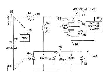
C~ 1 in parallel with the main bypass
inductor 62 and SCRs 64 and 66 is an auxiliary bypass path.
The auxiliary bypass path consists of a storage capacitor
68 connected in series with the parallel combination of a
"forward" conducting swiitching device 70 and a "backward"
rnn~ t;ng switching de~rice 72. Both switching devices 70
and 72 may be impl, n t~ as SCRs. As shown in Fig. 3, the
2 ~3i 76
--17--
storage capacitor 68 may be implemented as two
unidir~ctinn~l capacitors 74 and 76 connected in series,
with each capacitor 74 and 76 cnnnPct~ in parallel with a
diode 78 and 80, respectively. ~he anodes of the diodes 78
and 80 are connected together, and are al60 connected to
the node 82 where the capacitors 74 and 76 are cnnnpct~d
together. ~he resultinq bridge structure allows capacitor
74 to be charged from a positive voltage on the t~rmin~l~
54 and 56 by a current through diode 80, and capacitor 76
to be charged from a negative voltage on the t~rm;nAl~: by a
current through diode 78. A voltage clamp 84 is cnnn~ct~-d
aeross the capacitor 68 at t~ n~ 85 and 86. The
operation of the voltage clamp 84 will be described in more
dQtail below.
Under external system fault conditions, a voltage
transient will force the, voltage acro5s the hlork;n~
capacitor 58 to exceed z preset trigger level, e.g., 270
volts . This causes the SC~a 64, 66, 70, and 72 to be f ired
in a Sr~r~ nre which ultimately results in a low 1
path for the fault curre~nt through the main bypas6 path
SCRs 64 and 66, bypass path inductor 62, and inductor 61.
For il-~u~ LOL. 61 and 62 having a ~-in~ 60 Hz i - --
of about 4 milliohms, the peak voltage across the blocking
capacitor 58 will be kept to about ~2 X 27kA X 4mn - 153 V
under a maximum 60 llz fault current of 27kA.
If, at the initial triggering instant of a fault,
a reSIuisite stored voltage level does not already exist
aeross the storage capacitor 68, the auxiliary SCRs 70 and
72 are turned on prior to the main bypass path SCRs 64 and
66. This causes curren~ to flow to the auxiliary bypass
path and into the capacitor 68 which ~ yl,ULeS a
predetermined voltage level. This voltage stored in the
capacitor 68 will be used later to te of ~ any DC
current in the main SC~3 64 and 66 which may have built up
during the fault interval. Capturing a voltage on storage
capacitor 68 from the external system, e.g., the
transformer 32, connected to the t~rmin~l~ 54 and 56 avoids
_ _ _ _ _ _ _ _ _ _ _ _ _ _ _ _ , , , . _, .,, . ,, _,
2i$3~76
--18--
the need f or an i ~ rPn~ ~nt power source to charge the
capacitor 68. This makes it possible for the DC blocking
device 30 to be fully autonomou6. When the requisite
voltage leYel on the storage capacitor 68 is reached, the
main SCRs 64 an~ 66 are fired to provide a low 1 -
path for the fault current.
A more det~ 1 description of the operation of
the DC blocking device 30 in L~ e to a fault condition
i8 described with reference to Fig. 5. Prior to time to~
the AC current IAC~ flowing into the DC hlorkinq device 30
is normal . Since there is no DC current f low through the
capacitor 58 the total current 90 includes only an AC
, L. All of the SCRs, 64, 66, 70, and 72 are turned
off. The voltage across the DC hlorkin~ device 30 is IAC X
Xcl, where Xc~ is the; ~- of the blocking capacitor
58 .
At time to~ an over current begins to occur.
Shortly thereafter, at time tl, the voltage across the
hlf-rking capacitor 58 reaches the pr~ PtPrminp~l trigger
level. This i8 shown by the 6pike in the voltage waveform
91. At this point, the auxiliary SCRs 70 and 72 are turned
on to capture a prP~lPtPl~m; nP-l stored voltage level on
storage capacitor 68. The flow of fault current 92 through
the storage capacitor 68 and auxiliary SCRs, is ~hown in
Fig. 6. ~Iowever, this ~nly occurs if the storage capacitor
68 does not already hav,e the prp~lptprminpr~ voltage charge
level. If the storage capacitor 68 is already sufficiently
charged, the auxiliary SCRs 70 and 72 are not turned on to
charge the capacitor, instead, the main SCRs 64 and 66 are
turned on immediately after the trigger level is reached.
I~ the auxiliary SCRs 70 and 72 are turned on, once the
storage capacitor 68 reaches its stored voltage level,
e.g., 50V, the main SCRs 64 and 66 are fired. This results
in a low i -- nre bypass path between the tPrmin~l~ 54 and
56. The flow of fault current 92 is now through the
inductor 62 and main bypass path SCRs 64 and 66 as shown in
Fig. 7. Since the current to the auxiliary SCRs 70 and 72
2 1 ~ i 76
--19--
i5 now shunted through mai n SCRs 64 and 66, the auxiliary
SCRs, which are no longer receiving firin~ signals, are
deprived of current and t~lrn off, leaving the stored
voltage c~LuLcd on storage capacitor 68.
For simplicity, waveform details for thQ short
initial c~nr~ tinn period of auxiliary SCRs 70 and 72 are
not shown in Fig. 5. Fig~3. 8-10 are actual oscillograms of
the voltages across the blocking capacitor 58 and storage
capacitor 68 during the first two cycles of AC fault
_urL~:I.L-~ of 11.6, 17.6, and 27.2 kA rms, respectively.
Waveforms 100, 102, and 104 ~1 LL~te the capture of
voltage on the storage capacitor 68 at the triggering
instant . Note that the ~torage capacitor 6 8 becomes
quickly charged to the stored voltage level at the
beginning of the fault. Waveforms 106, 108, and 110
illustrate that the voltage across the blocking capacitor
58 uvcLal.ooLs the triggering level, e.g., 270V, even after
the main ScR~s 64 and 66 are f ired after the storage
capacitor 68 reaches its stored voltage level. The level
of the overshoot increasos as the fault increases. This
.I-oo~ is caused by t~le; ~ n. e (Ll + ~2) of inductors
61 and 62 which does not allow in-LallLd~eous transfer of
the fault current to the main SCRs 64 and 66 when they are
triggered. NotQ, however, that the peak voltage across the
SCR~s 64 and 66 themgelves, does not exceed the trigger
level. This is because the SCRs are turned on at the
trigger level, before the ovcLDllo~t voltage on the bl~l~ k;n~
capacitor 58 occurs. As can be seen from waveforms 106,
108, and 110, the volta~e across the bl-~ck;n~ capacitor 58
will oscillate for a period after the SCRs 64 and 66 are
triggered. Thig oscill~tion is caused by the C~/ tLI + ~)
es~ flL circuit formed by the hlnrkinq capacitor 58 and
inductors 61 and 6 2 .
R~tl~rninq now to Fig. 5, during the fault period,
the main SCRs 64 and 66 carry the fault current. The
voltage across the }~ ;nq device, shown by waveform 91
remains low, and, for simplicity, may be assumed to be 0.
218~l7~
. ~ .
--20--
At time t~, the external fault clears. At this point, the
main SCR6 64 and 66 are kept in conduction for a further
"cooldown" period. The cooldown period allows the SCR6 64
and 66 time to cool ~efor~ attempting to turn them off.
The ability of an SCR to turn off and block reapplied
voltage may be signif icantly degraded immediately after a
current surge, due to the high SCR ~unction temperatures
reached during the surge. After the cooldown period, and
after the control system of the blorkln~ device 30 checks
lo to ensure that the fault llas p~ n~ntly cleared, th~
conditions are satisfled ~or turning off the main SCRs 64
and 6 6 .
Due to the application of an external DC voltage
across the ~erminals 54 and 56 of the blocking device 30, a
DC ~ --,t of current IDC will have built up in the main
SCRs 64 and 66 during the fault and cooldown periods from
time tl to time t3. Thu6, the forward conducting SCR 64
will be stuck in conduction with a uni-directional
pulsating current, which is the sum of the DC current IDC
and the normal AC current IAC passing through it.
At time t3, the fault has pas~3ed, the cooldown
period is completed and the window for keeping the main
SCRs 64 and 66 in conduction is terminated. At this point,
the DC current ~ -n~t IDC must be removed from the ~ain
SCR 64 in order to commut:ate it off to return the blocking
device 3 0 to the DC current blocking state . Thus, at time
t3, the All~illAry SCRs 70 and 72 are fired. This causes the
pre-captured voltage on storage capacitor 68 to divert the
current from the main SC]~s 64 and 66 into the Aln~ Ary
SCRs 70 and 72. This extinguishes the c~n~ rtirn of the
main bypass path SCRs 64 and 66.
Fig. ll shows the initial and final current flows
through the blocking device 30 for commutation off of the
main SCR 64 in the case where the storage capacitor 68 wa~
charged "negatively" during the initial charging period
following the be7~nnin~ of a fault. The storage capacitor
68 will become negatively charged when the initial fault
_ _ _ _ _ _ _ _ _ . . _ _ _ _ _
21~i76
. ~ .
--21--
condition voltage at terminal 54 is negative with respect
to terminal 56. In this case, when the auxiliary SCRs 70
and 72 are fired, a reverse voltage from the storage
capacitor 68 is i ~sDed across the conducting main SCR
64, turning it off. The initial current flow 120 through
the main bypass path is thus re-directed through the
capacitor 68 and auxiliary SCR 70 to become the final
current flow 122.
Figs. 12 and 13 illustrate commutation of the
forward cnnA-lrt;nq main SCR 64 in the case where the
storage capacitor 68 has been pre-charged "positively"
during the initial charging period following the initiation
of a fault. The storage capacitor 68 may become positively
charged, for example, when the initial fault voltage at
terminal 54 is positive with respect to terminal 56. As
shown in Fig. 12, the initial current 120 is flowing
through the forward cnnS~lct;nq main bypass path SCR 64.
When the auxiliary SCRs 70 and 72 are fired, the stored
voltage in the storage capacitor 68 sends a forward
oscillatory current 124 through the forward main SCR 64,
the backward cnnrlll~rt;nq auxiliary SCR 72, and back into the
storage capacitor 68. At the end of a half cycle of the
oscillation, the voltage in the storage capacitor 60 har~
Le~,eLDed. At this point, as shown in Fig. 13, the, now
~ L~ed, voltage acros& the storage capacitor 68 is
essed across the corl~ducting main SCR 64 diverting the
current 120 from the SCF~ 64 through the storage capacitor
68 and forward connected auxiliary SCR 70 resulting in the
final current flow 122. Thus, the forward conducting main
SCR 64 is commutated of~ the stored voltage on the
storage capacitor 68 ex.eeds the pr~ t~m; n-~d stored
voltage level, e.g., 50~r, before the commutation process
begins, the control system o~ the DC hlnrkinq device 30
waits until the storage capacitor 68 discharges to the
3~ prP~t~m;n~-cl stored vo]tage level before -;nq
commutation. This is done in order to avoid excessive
amplitude on the oscillatory current 124.
2 1 8~ i 7S
--2 2--
It is also pref erable that the commutation
process be initiated only when the AC current in the
~1 ork ~ n~ device ig OppQ8 1 n~ the DC current in the device .
This reduces the amount of current which must be removed
from the main SCRs to turn them of f .
During the fau~t and cooldown periods, time tl to
time t3, during which the main bypass path SCRs 64 and 66
are conducting, DC energ~r, from stray or applied DC voltage
on the external system to which the DC blocking device 3 0
is attached, ~ay become stored in the 6ystem inductances
Lsys of the external system. For example, such DC energy
may become stored on the windings 38 of the transformer 32
to which the DC blol king device 30 i6 attached, as shown in
Fig. l. The DC energy sl:ored in this case will be:
l/2LsysIl~c2~ (DC energy c~n simila~ly become stored in the
inductances 61 and 62 of the blocking device 30 itself . )
This stored DC energy causes the voltage across the
blocking device 3 0 to rise once the main bypass path SCRs
64 and 66 have been turn~d off. The voltage rise may
result in false re-triggering of a fault hAnAl in~ se~uence
by the blocking device 3 ~ . Thus, the stored energy can
cause continuous cycling into and out of fault operations.
The current in the system inductances may also be forced
through the inductor 61, the storage capacitor 68 and the
forward connected A~ ry SCR 70, preventing turn-off of
the SCR 70. Some current will also flow in the hlo~ n~
capacitor 58.
To deal with these potential problems, a clamp
circuit 84 is preferably provided. Whe~ the stored DC
energy causes the voltage across the hlo~kin~ device 30 to
reach a certain level, the clamp circuit 84 prevents a
further rise in the voltage beyond this clamping level. As
shown in Fig. 14, the current flow 126 is directed through
the voltage clamp 84 and the forward conducting auxiliary
SCR 70 during the clamping period. The active voltage
clamp 84 bypasses the c~rrent 126 into a resistor, which
dissipates the stored sy stem energy . The voltage across
_ _ . . . _ _ = = = = = _ _ =
2 ~ 76
--23--
the clamp 84, VCI~AP~ is much higher than the PYt
applied or stray DC fault voltage. Since the sy6tem
; nr~ t~nre Lh.S is typical ly much higher than the inductance
of inductors 61 and 62, L~ + L2, the stored DC current will
be effectively decreased by the clamp 84 at a rate of
VC~Up/Lsy~ amps/6.
The active vol1:age clamp 84 is described in more
detail with reference to the schematic circuit diagram of
Fig. 15. Resistors 130 and 132 form a voltage divider
across the tprm; nAl R 85 dnd 86 of the clamp 84 . The values
of the resistors 130 and 132 are 5PlP~'l Pd such that when
the voltage across the clamp terminals 85 and 86 is less
than the clamping voltag~e level, e.g., 220V, a voltage
level is 2pplied to the positive terminal of a comparator
134 which is less than the voltage applied to the negative
terminal of the comparator 134 as set by the zener diode
136. Thus, when the voltage acros6 the tprminAlc: 85 and 86
i5 less than the clamp voltage level, th~ output of the
- Lor 134 is ;~pproximately 0 volts . The output of the
c.Lor 134 i5 connected to the gate of a switching
device, such all a insulated gate bipolar tr~nsistor (IGBT)
138. A low input voltage on the gate of the transistor 138
ensures that the transistor 138 will be turned off, and
will not be c~ t;ng any current.
When the voltage across the clamp tprminAl~ 85
and 86 exceeds the clamp voltage level, during the clamping
period, the voltage on ~he positive input of the . Lur
13~ eYceeds the voltage on the negative input of the
lltUL 134 and the output of the ~- ~Lor becomes
HIGH. This turns on th~ trangistor 138, c-~nnPctin~7
resistor 140 in series with diode 142 across the tPrminAlR
85 and 86. Current is thus conducted through, and
dissipated by, the resistor 140. Hysteresis in the
comparator 134 keep!3 the transistor 138 on until the
voltage across the tPrm;nAlR 85 and 86 falls below a lower
clamping level, e.g., 180V.
218~l76
--24--
As shown by the waveforms of Fig. 16, the storage
capacitor 68 acts in concert with the active clamp circuit
84 to produce a voltage waveform 91 across the blocking
device 30 that D~wLo~,Ll-s between the upper clamp voltage
level, 220V, and the lower clamp voltage level, 180V.
Thus, the storage capacitor 68 has a dual role. It i5 used
to commutate current from the main SCRs 64 and 66 to turn
them o~f after a fault period, as well as serving as an
integral part of the cla~p circuit 84. It can be seen that
the active clamp 84, as ~;hown, has an effective constant
average clamp voltage value of 200V, the average of 180V
and 220V. This clamp voltage level is ;n,lPr~n,l~-nt of the
value of the DC current, I~c. Maintaining the clamp voltage
at a constant average value of the current is desirable as
this min;mi7~: the fall t:ime of the DC current as shown by
waveform 146 in Fig. 16.
The clamp circuit 84 shown in Fig. 14 is
unidirec~inn~l, i.e., only positively oriented voltages
will be clamped, and positively directed currents will be
dissipated. For various applications, a bi-direct;nn~l
clamp may be pre~erred. Such a bi-dirP~ t~;nn~l clamping
circuit may be i ~1~ L~d using two clamp circuits 84 as
shown in Fig. 14 connect~Qd in anti-parallel. The resulting
bi-directional clamping ~ircuit will dissipate inductive
~:u~- . .ts flowing in either direction through the b]n~ k;nq
device 3 0 .
The purpose of the resistor 144 and zener diode
146 i5 to discharge slowly excess voltag~ across the
storage capacitor 68 after the clamp period has finished.
The breakdown voltage of the zener diode 146 is set to
egual thQ desired stored voltage level in the capacitor 68.
Thus, when the voltage across the capacitor 68 eYceeds this
level, the zener diode 146 will conduct current through the
resistor 144 which will dissipate the excess energy. The
resistor 144 and zener diode 146 also act to remove eYCes6
voltage on the storage capacitor 68 if the voltage captured
on the capacitor 68 durlng initial triggering of thQ
_ _ _ _ _ _ _
21~ 76
--25--
hlo~rin ~ device 30 overshoots to a level higher than the
prPri~fo~n;n~l stored voltage level.
Returning once again to Fig. 5, at time t4 the DC
~ of the current through the blocking device 3 0
reaches 0. Thus, all the DC energy stored in the system
inductances has been re~loved . The f orward conducting
auxiliary SCR 70 turns off naturally, since it now has
become deprived of current. The residual AC system
current, IAC~ diverts in its entirety from the auxiliary
bypass path to the DC b3 ocking capacitor 58. The voltage
across the hl~-kin~ device 30 returns to its normal value.
The storage capacitor 6~ initially remains charged to the
clamping level VCL~ but is 810wly discharged to the
residual voltage storage level by action of the resistor
144 and zener diode 146 Operation of the hl~-kin~ device
30 then returns to its original pre-fault state, i.e.,
bef ore time to-
A preferred ' '; L of a control system 150
for the DC hlockinq device 30 of the present invention is
described with reference to Fig. 17. Though shown
l ~ Led with discre1:e logic ,_ Ls, the control
system 150 for the hlo~-lrinJ device 30 may also be
implemented using, for ~axample, ~LVyL hle logic devices.
The control logic syste~1 for the blocking device 30 may
also be implemented, in whole or in part, using a software
hle microprocessor or similar device.
Power for the logic and firing circuits of the
control system 150 may preferably be provided by an
; nti-~r~nri~nt power 8upply (not shown) . Alternatively, power
for the control system may be provided by the fault
currents themselves. Tllerefore, since power for
commutation of the main SCRs 64 and 66 is also provided by
the fault current, as s~ored in storage capacitor 68, the
entire hlor~lr;n~ device of the presenf invention 30 may be
made autonomous, i.e., ~ithout the need for any auxiliary
power supply. An autonomous blocking device 30 is
particularly suitable to applications in remote locations.
2 1~ 1 76
--26--
In an autonomous blocking device 30, the control 6ystem 150
may be powered durinq the initial period following the
initiation of a fault fro~n energy stored in the main
hlo-~king capacitor 58. Oalce the storage capacitor 68,
which is much larger than the blocking capacitor 58, is
fully charged by the fault current, power for the control
system 150 may be obtained from the energy stored in the
storage capacitor 68. The energy stored in the storage
capacitor 68 will typically be sllff-icipnt both to power the
control system 150 through the fault hAn-ll ;n~ period and to
commutate off the main SCRs 64 and 66 after the fault has
passed .
The control logic circuit 150 i n~] ll~oC monostaole
timing circuits 152, 154 and 156. In normal operation,
monostables 152, 154 and 156 have a logic 1 input and a
.L~ ling logic 0 output. When the input is driven to
logic 0, the output beco~e6 logic 1. The output remains at
logic 1 until a sQt time after the input returns to logic
1, at which time the outL~ut returns to logic 0.
Monostable timing circuits 158, 160, 162, 164,
166 and 167 also have a logic 1 input and uLL~iuull.ling
logic 0 output in normal operation. When the input of
these monostables is driven to logic 0, the output becomes
logic l. The output remains at logic 1 for a set time
after the input first becomes logic 0. The output then
return6 to logic 0 until the next transition of the input
f rom logic 1 to logic 0 .
Voltage sensing circuit 168 has a logic 1 output
when the voltage across the DC blocking capacitor 58
eYceeds the fault trigger level, e.g., 270V. The voltage
sensing circuit 168 has a logic 0 output when the voltage
across the DC h1~ ;n~ capacitor 58 ~s less than the fault
trigger level.
Voltage sensing circuit 170 has a logic 1 output
at terminal A, and a logic 0 output at terminal /A, when
the voltage across the storage capacitor 68 is greater than
the prPdPtPrm; nP~ 6tored voltage level, e. g ., 50V . When
`` 2~3176
--27--
the voltage across the Etorage capacitor 68 is less than
the stored voltage level, the /A output of voltage sensing
circuit 170 is loqic l, and the output A of voltage sensing
circuit 170 i5 logic 0.
The voltage sensing circuit 172 has a logic l
output when the voltage across the main bypass path SCRs 64
and 66 is greater than a, re-triggering level, e.g., 20V.
Voltage sensing circuit 172 has a logic 0 output when the
voltage across the main bypass path SCR3 64 and 66 is less
than the re-triggering level.
The voltage sensing circuit 174 has a logic 1
output when the voltage across the forward conducting
auxiliary SCR 70 is greater than a set level, e.g., 5V.
Voltage sensing circuit 174 has a logic 0 output when the
voltage across the forward crn~ tinq auxiliary SCR 70 is
less l;han the set level
Current sensiIIg circuit 176 has a logic 1 output
when the system AC current through the hl~ inq device 30
is greater than the maximum normal value, e.g., 120 AC rm3.
Current sensing circuit 176 has a logic 0 output when the
system AC current is less than or equal to the maximum
normal value.
Current sensing circuit 178 delivers a logic 1
output when the AC current through the hlo-~kinq device 30
is in~L~.. L,Iilevusly posil:ive, i.e., current is flowing into
the blocking device 30 ~hrough terminal 54 and out of the
hlorlrinq device 30 throllgh terminal 56. The current
sensing circuit 178 has a logic 0 output when the AC
current through the DC l~lo- kinq device 30 is
3 0 instantaneously negative.
Each of the voltage sensing circuit5 168, 170,
172 and 174 and current sensing circuits 176, and 178 may
be implemented as convelltional voltage and current sensing
circuits which are knowL~ to those having skill in the art.
SCR firing circuits 180, 182, and 184, deliver
isolated firing pulses to the backward conducting auxiliary
SCR 72, the forward con~ucting auxiliary SCR 70, and the
2~8~176
.
--28--
main bypass path SCRs 64 and 66, respectively. The firing
circuits 180, 182 and 184 deliver isolated firing pulses at
their outputs to their respective SCRs in rc~,~uu..se to logic
1 signals at their inputs. The firing circuits 180, 182,
and 184 may be of a conventional design.
During normal operation, i.e., not during or just
after a fault condition, the outputs of the monostables
160, 162, 166 and 167 are logic 0. Thus, the inputs to the
firing circuits 180, 182 and 184 are logic 0, and no firing
pulses are delivered to the SCRs 64, 66, 70, and 72.
During normal operation, the voltage Vcl acrosg the hlot-k;n7
capacitor 58 is less than the fault triggering level,
therefore, the output of voltage sensing circuit 168 is
logic 0. The outputs of the other monostable circuits 152,
154, lS6, 158, and 164 are also at logic 0.
When a fault occurs that increases the voltage
level across the blocking capacitor 58 to the triggering
level, the output of voltage sensing circuit 168 becomes
logic 1. The output of voltage sensing circuit 168 is
passed through inverter 188, appearing as a logic 0 input
to monostable circuit lS8. Thus, the output of monostable
circuit lS8 becomes logic 1. I~ the voltage Vcl across the
storage capacitor 68 is less than the prP~lPtPrmi"Pd stored
voltage level, e.g., so~r, the output /A of voltage sensing
circuit 170 will be logic 1, making all the inputs to the
AND gate l90 logic 1. ~Recall that the output of
monostable lS2 is logic 0 during normal operation, which
signal is inverted by inverter 191. ) The output of the AND
gate 190, will thus become logic 1, causing differentiator
circuit 192 to generate a positive going pulse which is
inverted by inverter 194. This causes the input to the
monostable circuit 160 t:o be driven to logic 0 for a period
~PtPr~ninPd by the diffel-entiator 192. The output of
monostable circuit 160 t:herefore becomes logic 1, for,
3S e.g., 10 mi- . ,g~ . This pulse is delivered to the ûR
gates 196 and 198. The logic 1 on the ûR gates 196 and 198
causes a firing pulse to be delivered via firing circuits
21~3176
,
--29--
180 and 182 to the auxiliary bypass path SCRs 72 and 70,
respectively. Note that while the output of monostable
circuit 160 is at logic 1, the output of thQ inverter 200
is logic 0. This prevents a logic 0 from appearing at the
output of NAND gate 202, and at the input of monostable
circuit 167. Thus, monostable circuit 167 is positively
prevented from initiating a firing pulse from firing
circuit 184 to the main b~pass path SCRs 64 and 66 while
the auxiliary bypass path SCRs 70 and 72 are being fired.
As soon as the storage capacitor 68 charges to
the stored voltage level, the output /A of voltage sensing
circuit 170 becomes logic 0. Shortly thereafter, the
output A of voltage sensil~g circuit 170 becomes logic 1.
The outputs of voltage sel~sing circuit 170 do not change
simultaneously in order to provide a short rl~A~lhAnA to
ensure that the main SCRs 64 and 66 and auxiliary SCRs 70
and 72 are not fired simultaneously. At this point, the
output of monostable circuit 158 is still logic 1. Thus,
the output of AND gate 204 becomes logic 1. This causes
the output of NOR gate 206 and the input to monostable
circuit 152 to become logic 0. This causes the output of
monostable circuit 152 to become logic 1, the output o~ NOR
gate 208 to become logic 0, and the output of inverter 210
to become logic 1. At this point, the output of the
inverter 200 is also logic 1 as is the output of voltage
sensing circuit 172, since the insta~,L~ us voltage across
the main bypass path SCRæ 64 and 66 is the fault voltage
level, which is greater than the pre-set re-triggering
level, e.g., 20 V. Thus, the output of NAND gate 202
become logic 0, causing monostable circuit 167 to deliver a
logic 1 input pulse to the SCR firing circuit 184. In
turn, the firing circuit 184 causes firing pulses to be
delivered to the main bypass path SCRs 64 and 66.
Waveforms illustrating the relationship between
the voltage across the main bypass path SCRs 64 and 66
(waveform 203), the outp~t signal from the monostable
circuit 158 (waveform 205), and the voltage across the
2~83176
, .
--30--
storage capacitor 68 (waveform 207), are shown in Fig. 18.
At time tlo the output of monostable 158 goes to logic 1,
initiating triggering of the auxiliary SCR6 70 and 72.
This connects the storage capacitor 68 across the inputs of
the blocking device 30 via the inductor 61, causing the
capacitor 68 to begin the charge from the fault current.
Since the fault current is now flowing through the
auxiliary bypass path, the voltage across the main sCRs 64
and 66 immediately drops, then begins to increase with the
voltage across capacitor 68. At time t~l the voltage on
capacitor 68 has reached the stored voltage level. Thus,
the auxiliary SCRs 70 and 72 are turned off, stopping the
voltage rise on capacitor 68, and the main SCRs 64 and 66
are turned on, causing the voltage across them to drop to
zero. At t~2, after the predetermined delay of the
monostable circuit 158, the output of monostable 158
returns to logic 0.
The pre-de~QrminP~l delay of monostable 158 is
more than sufficient to allow the voltage on the storage
capacitor 68 to reach the stored voltage level, resulting
in a change in the outpu~s of voltage sensing circuit 170
which, in turn, initiate~ firing of the main ScRs 64 and
66. If the storage capacitor 68 faLls to charge, or the
voltage sensing circuit 170 fails to indicate that the
storage capacitor 68 is l~harged to the stored voltage
level, the return of the output of monostable 158 to logic
0 will cause differentiator 209 to output a negative going
pulse which is inverted by inverter 211. The positive
pulse output of inverter 211 activates NOR gate 206,
initiating firing of the main scRs 64 and 66. Thus, the
delay of monostable 158 ~Qt~rminQ-~ the maximum allowed time
for voltage sensing circuit 170 to indicate that the
storage capacitor 68 has been charged to the stored voltage
level. If the output of voltage sensing circuit 170 does
not ch~nge within the allowed time, a failure is assumed,
and the return of the output of monosta~le 158 to logic
zero initiates f iring o~ the main sCRs 64 and 66 to provide
21~ 76
--31--
a low i mrt~ n~-e path across the blocking device 3 0 . Thus,
a failure of the voltage sensing circuit 170, for example,
will not result in a fail~re of the blocking device to pass
f ault current through the main bypass path .
When thQ main ~ypass path SCRs 64 and 66 fire,
the voltage across them falls below the firing voltage
level. Thus, the output of voltage sensing circuit 172
becomes logic 0. This ca~lses the output of NAND gate 202
to become logic 1, and prevents further firing pulses from
being delivered by the firing circuit 184 as long as the
voltage across the main b~rpass path SCRs 64 and 66 remains
less than the re-triggerillg voltage of 20 V.
So long as the f ault condition remains, the
output of monostable circuit 152 remains at logic 1. This
causes the output of inve~-ter 210 to also remain at logic
1. II~L=UVC:L, the output of inverter 200 remains at logic 1
through the fault because the output of the monostable 152
is inverted by inverter 1~1 to assure that the output of
NAND gate 190 remains at logic 0, preventing f iring of the
auxiliary SCRs 70 and 72 via monostable circuit 160. ~hus,
a window for firing of thl~ main bypass path SCRs 64 and 66
is maintained. New f iring pulses are delivered to the main
bypass path SCR~ 64 and 66 each time that the current
through the main bypass path f alls to 0 and tries to
reverse. When the AC fault current through the SCRs 64 and
66 falls to 0, the SCRs commutate off. Thus, when the
current L~_ =,es on the opposite half of the cycle, the
voltage acro~s the SCRs 64 and 66 rapidly increases to the
re-triggering level set by the voltage sensing circuit 172.
This causes the NAND gate 202 to produce a logic 0 output.
In turn, monostable circuit 167 initiates a new firing
pulse to the main SCRs 64 and 66 through the firing circuit
184 .
Therefore, after the initial firing of the main
bypass path SCRs 64 and 66 at the fault triggering level,
270V, the bypass path SCRs 64 and 66 are fired each time
that their anode voltage exceeds the re-triggering voltage
I , 21~76
--32--
level, 20V. Holding back firing until the voltage reaches
20V ensures that all par211el bypass path SCRs, as shown in
Fig. 4, are fired, even at moderate levels of fault
current. A side effect of the 20V firing threshold is that
it creates a local oscil latory current, of about 300 amps
peak, through the inductors 61 and 62. If the external
fault current is low, this local oscillatory current can
periodically reduce the net current through the SCRs 64 and
66 to 0, thereby naturally turning off the main SCRs 64 and
66 after about 1.5 ms. Re-triggering will occur, however,
when the instantaneous voltage again exceeds the re-
triggering level 20V. If the externally applled fault
current is more than a few hundred amps, the main SCRs 64
and 66 will stay in cr~nrillr~tie~n for the full 60 Hz half
cycle of the f ault current . This is because the
oscillatory current ~LUd~'.'ad by the 20 V firing threshold
in such a case will not be suf f icient to peri o~l 1 r 111 y
reduce the current throllgh the SCRs 64 and 66 to zero,
therefore, they will re~ain in cAn~ rti-~n
The output of monostable circuit 152 is fed as an
input to the AND gate 212. The other input to AND gate 212
i5 the output of OR gate 214. Thus, once the output of
monostable circuit 152 ]~ecomes logic 1, it stays at logic
so long as the output oE OR gate 214 is logic 1. This is
because a logic 1 outpu~ on OR gate 214 results in a logic
1 output on AND gate 212 and a logic 0 output on NOR gate
206 which keeps the out]?ut of monostable 152 at logic 1.
The output of OR gate 214 is logic 1 so long as the AC
current through the hlo~ ; nq device 3 0 is greater than
normal, the voltage Vc~ across the storage capacitor 68 is
greater than the pre-determined stored voltage value, or
both. So long as the AC current in the hlorkinq device 30
is greater than the nor~al value, the output of current
sensor 176 is logic 1. Also, as described earlier, so long
as the voltage across the storage capacitor 68 is greater
than the pre-~ete~min~cl stored voltage value, the A output
of voltage sensing circuit 170 is logic 1. Thus, the
r 2 i ~3~;1 7 6
--33--
output of monostable 152 is kept at logic 1, and the firing
window for the main bypa6s path SCRs 64 and 66 is
maintained, until the AC current has rsturned to normal and
any excess voltage abov~ the stored voltage level on
storage capacitor 68 ha~ been dissipated. The f irst
conditionr requiring a return to normal AC current, ensures
that the cooldown perio~ for the main SCRs 64 and 66, as
set by monostable 152, is started only after the fault has
cleared. The second condition, requiring no excess voltage
on storage capacitor 68, is necessary to avoid excessive
current from the storage capacitor 68 when firing the
auxiliary SCR6 70 and 72 to commutate off the main SCRs 64
and 66.
Once these two conditions have been met, the
output of AND gate 212 goes to logic 0, the output of NOR
gate 206 goes to logic 1, the input to monostable circuit
152 goes to logic 1, and a cooldown period, e.g. of 2.5
seconds, i3 initiated. The duration of the coo~ ., period
is set by the monostable circuit 152. The output of the
monostable circuit 152 qoes to logic 0 after the cooldown
period. This sets the stage for termination of the firing
window for the main bypass path SCR6 64 and 66.
The output of monostable circuit 154 is connected
via AND gate 216 as an input to NOR gate 208. The other
input to the AND gate 216 is the output of the current
sensing circuit 178, which provides a logic 1 signal when
the current through the h~lockin~ device 30 is positive.
Thus, when the output of monostable circuit 152 goes to
logic 0, the input to monostable circuit 154 goes to logic
1 if the output of the current sensing circuit 178 is logic
0 at the same time. Otherwise, the input to the monostable
circuit 154 goes to logic 1 as soon as the output of
current sensing circuit 178 goes to logic 0. This will
occur as soon as the next negative half cycle of the
current through the hlo~ k~n~ device 30 begins. Since the
output of monostable circuit 154 going to logic 0 controls
the initiation of turn-of f of the main bypass path SCRs 64
_ _ _ _ _ _ _ _ _ _ _ _ _ _ _ _ _
2 ~ 83 i 76
--34--
and 66, the requirement f~r the output of the current
sen6ing circuit 178 to be logic 0 before turn-off is
initiated a6sures that the commutation of current in the
main bypass path SCRs 64 and 66 cannot take place during a
positive half cycle o~ the AC system current when the AC
current would be in addition to any DC current through SCRs
64 and 66.
The output of monostable circuit 154 going to
logic 0 controls the initiation of firing pulses to the
auYiliary SCRs 70 and 72. The built in delay of the
monostable circuit lS4, e.g., 1.3 ms, a3sures that the
output of the circuit 154 won't go to 0 for a period after
the firing window for the main SCRs 64 and 66 is terminated
by the output of monosta~le circuit 152 going to logic 0.
During this delay period, the main SCR6 64 and 66 are left
without f iring pulses . This ensures that no f iring pulses
for the main SCRs 64 and 66 are pre6ent when the auxiliary
SCRs 70 and 72 are fired. This, in turn, avoids the
p~t~;hil;ty for high internal circulating current and
~ tion failure.
When the output of monostable circuit 154 goes to
logic 0, the input to monostable circuit 156 goes to logic
1 through action of the inverter 218. A set time later,
the output of monostable circuit 156 goes to 0. (Note that
monostable 156 merely adds an extra delay which may be
eliminated. ) This cause~; the output of the differentiator
220 to deliver a logic 0 pulse to the inputs of monostable
oircuits 162 and 164. T~lis causes the output of monostable
circuit 162 to become logic 1 ~or 20 mi~:L~ e~ , causing
a 20 mi.:Lv~e~ d firing pulse to be delivered to the
backward c~n~ ;n~ auxi:Liary SCR 72 by firing circuit 180.
Simultaneously, the output of monostable circuit
164 becomes logic 1 for a set period, e.g., between about 2
and 7 second6. During t}lis period, the forward connected
auxiliary SCR 70 is free to conduct. This allows for
connection of the voltage clamp circuit ~4 into the DC
blocking device 30. PreEerably, this voltage clamping
218~t76
--35--
period is adjustable, providing fl~Yih; l 1ty for
optimization of the cla3Ilping period to suit the particular
external system parameters. Throughout the period that the
monostable circuit 164 has a logic l output, the output of
the NAND gate 222 will be driven to logic 0 by the voltage
sensing circuit 174 whic.h ~3 oduces a logic 1 output when
the voltage across the 3Eorward rnn~ rt;nq auYiliary SCR 70
eYceeds a selected voltz,ge level, e.g., 5V. When the
output of NAND gate 222 goes to logic 0, the output of
monostable circuit 166 initiates a 20 us firing pulse to be
delivered to the forward cnn~tllrt-;nq auxiliary SCR 70 by the
firing circuit 182. Thus, a 20 ,us firing pulse is
delivered to the forward conducting auxiliary SCR 70
vu3L the voltage across it exceeds 5 V. This ensures
that the forward rnn~lllrt-inq auxiliary SCR 70 keeps the
clamp circuit 84 c f~ throughout the clamp period
Y~:L positive current wants to flow into the clamp
circuit. I3t a bi-direc~t innAl clamping circuit is employed,
a similar ~ may be used to fire the backward
connected auxiliary SCR 72 to keep the clamp circuit
connected through the clamp period lr~lle:llt:Vt:L either positive
or negative current wan1:s to f low in the clamp circuit.
When the output of mono6table circuit 164 goes to
logic 0, the output of IJAND gate 222 is disenabled. Thus,
further firing of the forward cnn~llrtinq auxiliary SCR 70
i5 prevented, r3i~ ing the voltage clamp 84 from the
hlorkinq device 30. At this point the state of the control
system circuit 150 retu3^ns to its state prior to the
initiation of the fault.
Under fault conditions, triggering of the main
bypass path SCRs 64 and 66 and the auxiliary SCRs 70 and 72
is initiated via a cont rol system such as that shown in
Fig. 17. The control system sends timing signals to the
main firing circuits 180, 182 and 184, which, in turn, send
i~olated firing pulse6 to the gates of the SCRs 64, 66, 70,
and 72.
2 l~i 76
, .
--36--
Preferably, th~e DC blocking device 30 is provided
with backup f iring circuits f or the main bypass path SCRs
64 and 66 . The backup f iring circuits will f ire the main
SCRs 64 and 66 only in abnormal circumstances, namely, in
the event that the main firing circuits 180, 182, and 184
fail to deliver the firing pulses. This failure may occur
due to failure of the control system 150, failure of one or
more of the main firing circuits 180, 182, or 184, or a
failure of the supply of power to the control system 150 or
the firing circuits. The function of the backup firing
circuits may be restricted to simply f iring the main SC~s
64 and 66 to prevent a voltage rise across the hl ~ i nq
device 30. In this situation, it may be acceptable that
the main SCRs 64 and 66 remain in c~ rti~n after a fault
clear~i, due to inability to turn off due to DC follow-
through current. Preferably, the backup f iring circuits do
not rely on any auxiliary power source. The backup f iring
circuits may, therefore, be powered directly from the
rl~nl~: anodE ~ ode voltage across the main SCRs 64
Z0 and 66.
Preferably, multiple sets of backup firing
circuits are provided. The relative voltage levels at
which these backup f iring circuits may come into action is
described with reference to Fig. 19. This chart shows the
maYimum allowed DC voltage during normal operation 230 at
50 V, the permissible peak AC voltage 232 at 130 V, the
average voltage 234 across the voltage clamp 84 at 220 V,
the normal triggering level 236 at 270 V, the triggering
level of a primary back~p firing circuit 238 at 330 V, and
the firing level of a secondary backup firing circuit 240
at 420 V. Thus, the primary backup firing circuits may be
set to fire at an ar.o~ t~ode voltage across the main
SCRs 64 and 66 approximztely 229~ higher than the normal
trigger level set by the main control system 150. The
secondary backup firing circuit may be set to fire at an
~l~odE ~_dL~ode voltage, æpproximately 27% higher than the
voltage required for triggering by the primary backup
2i~ 76
,
--37--
f iring circuit . O~ course, the voltage levels provided in
Fig. 19 may be adjusted for the requirements of particular
applications of the DC b3 ocking device 30 of the present
invention .
So long as f iri ng of the SCRs 64 and 66 occurs
via the main control syst:em 150, the backup firing circuits
are inoperative. If, however, the main firing r- ' iF-
fails, the main bypass path SCRs 64 and 66 will be fired by
the primary backup f iring circuit, and the secondary backup
firing circuit will remaLn inoperative. If the main firing
'~nic-- and the primar~r backup firing system both fail,
then the main SCRs 64 and 66 are f ired by the secondary
backup f iring circuit.
A preferred primary backup firing circuit 250 ~or
the DC hl~ king device 30 is described with reference to
the schematic circuit diagram of Flg. 20. The tP~-m;nAlc
252 and 254 are cr~nnP~-~P~l across the main bypass path SCRs
64 and 66. The peak anod~ c ~LIlode voltage across the main
SCRs 64 and 66 is thus captured on capacitor 256 via diodes
258 and 260. If, under fault conditions, the main firing
circuits 180, 182, and 1~4 have failed to fire, the peak
voltage across the capacitor 256 will exceed the first
backup triggering level causing the zener diode 262 to
conduct. This will cause a voltage to appear at the gate
of the switching device 264, e.g., a MOSFET, turning it on.
In turn, the gate of the transistor 266 will be c-~nnPCtP~
to the common line 267 t~lrough transistor 264, turning it
on. This causes a voltage to appear on the gate of
transistor 268, turning it on as well. This causes a
firing current to flow f1-om capacitor 256, through resistor
270, the transi6tor 268, the resistor 272, and diode 274 to
the terminal 276 which i3 C-----P~ LP~l to the gate of a main
bypa6s path SCR 64 or 66 Thus, a backup firing pulse is
provided from the energy stored on the capacitor 256, which
also provides the power ~'or the backup firing circuit 250
itself .
21~ 76
, .
--38--
As was describe~ earlier, the high power DC
hlo--k1i-1g device of the present invention preferably
includes multiple bypass path SCRs connected in parallel
for each direction of current, as shown in Fig. 4.
Although the trigger levels of the backup f iring circuit
for each parallel SCR are n- in~l ly the 6ame, small
differences inevitably eYist. Thus, in the absence of
additional circuitry, when the trigger level for the first
to fire SCR is reached, that SCR will fire, preventing
further rise of the anode voltage of the other, paralleled,
SCRs . Thus, the backup f iring circuits of the other SCRs
will not reach their trigger levels, and will never fire
their SCRs. This i5 undesirable, since the one SCR which
fires will be required to carry the entire fault current
intended to be carried by multiple SCRs in parallel. This
could readily damage the SCR required to carry the current.
The r~nnc" ti~n of multiple primary backup firing
circuits for parallel c~nnoct~c~ main SCRs i8 shown in Fig.
21. To avoid the problem caused by one of the backup
firing circuits 250a-c firing before the others, an output
pulse associated with th~ firing of the backup firing
circuit is fed from each backup firing circuit to an input
of the next circuit to form a circular chain. Thus, for
example, an output pulse is fed on lines 278 and 279 from
backup firing circuit 250a to backup firing circuit 250b
when circuit 250a fires it3 SCR 64a. Lines 280 and 281
carry an output pulse from backup firing circuit 250b to
backup firing circuit 250c when firing circuit 250b
provides a firing pulsQ to its main SCR 64b. Finally,
lines 282 and 283 carry a pulse ~rom backup firing circuit
250c to backup firing circuit 250a when circuit 250c
delivers a firing pulse t:o it~l main SCR 64c.
The output pulses of each primary backup f iring
circuit is received via an opto-isolator 284 at the input
of the next backup firing circuit in the chain, as shown in
Fig. 20. When a pulse is received at the t~rmin~ 286 and
288 of the opto-isolator 284, a voltage is delivered to
,, 21~i76
--39--
turn on tran6istor 264, which, as described earlier,
results in a firing pulse being deliYered at terminal 276
of the backup firing circuit 250 which, in turn, is
connected to the gate o~ a main SCR. Note that this also
causes a voltage to appear on the tprminAlc 290 and 292,
which are the tPrminAl~ which are connected, via the
configuration shown in Fig. 21, to the opto-isolator
tPrminll~ of the adjacent primary backup firing circuit.
This intt:L.~ , P~ I ;on of primary backup firing circuits
ensures that all primary backup ~iring circuits generate an
output f`iring pulse. Thus, all of the main SCRs will turn
on, regardless of which S~R triggers first.
The 05~;11 n~ram shown in Fig. 22 shows the
voltage waveform 294 across the hlori-;n~ capacitor 58 o~
the blocking device 30 wh,en the main SCRs 64 and 66 are
fired by the primary backup firing circuit 250. To make
this waveform, the main firing circuits 180, 182 and 184
were ~ Ah1ad~ A fault c~rrent of 17 . 6 kA was then applied
to the blo~ ;n~ device 30. Note that the continuing
oscillation of the voltag,~ acros~s the hlo~kin~ capacitor
58, in combination with inductors 61 and 62, is due to the
main SCRs 64 and 66 being continually re~ired by the
primary backup firing circuits 250. The primary backup
firing circuits will re-trigger the main SCRs only when the
primary backup trigger level, e.g., 330V, is reached each
half cycle. Thus, the re3ulting oscillations are quite
significant, at least as ~ .:d with the minor continuous
oscillations resulting fr~m continual re-firing of the main
SCRs at 20V when they are fired by the control system 150
and main firing circuits 180, 182 and 184. Note also that,
since the primary backup firing circuits 150 do not apply
any firing pulses to the auxiliary SCRs 70 and 72, no
voltage will be ~ yLuLe:d on the storage capacitor 68, as
shown by waveform 296 in Fig. 22.
A preferred Pmho~li of a secondary backup
firing circuit 300 is described with reference to the
schematic circuit diagram of Fig. 23. The secondary backup
2 ~ ~ 3 i 7 6
--40--
firing circuit 300 is t~onnpctpd at tPnmin~lc 302 and 304
between the anode and cathode of the SCI~, e.g., SCR 64,
which it is to f ire . When the anode-cathode voltage of the
SCR 64 exceeds the breakover voltage of the series string
of zener diodes 306-311, current flows from the anode
terminal 302 through terminal 312 of the secondary backup
firing circuit 300 to the gate of the SCR 64, turning the
SCR on. One backup secondary firing circuit 300 i5
provided for each parallel ~nnnpct~d SCR in the blocking
device 30.
While all secondary backup firing circuits 300
have r ;n 11 ly the same trigger voltage, one backup firing
circuit for the parallel SCRs inevitably will fire first.
This will cause the voltage across the other paralleled
SCRs to drop, preventing the other SCRs from being turned
on by their secondary backup f iring circuit . This is
considered acceptable in this case. The secondary backup
firing circuit only operates if both the main firing
circuits and the primary backup firing circuits fail to
2 0 operate . The purpose of the secondary backup f iring
circuit is as almost a last resort backup to prevent
excessive volts from being developed across the hlorkintJ
device 3 0 under highly abnormal circumstances . It is
accepted that under these abnormal conditions the main SCRs
64 and 66 may be destroye~ and become shorted. The very
last resort to avoid exce~sive voltage across the blocking
device 30, if even the ~,e~ y backup firing circuits 300
should fail to operate, i~ anode breakover of the SCRs 64
and 66 themselves.
Since the basic purpose of the DC hlo~ inq device
30 of the present invention ig to restrict flow of DC
current, it is important to ensure that the device 30 is
performing this function properly. This is preferably
accomplished by continually monitoring the current through
the blocking device 30 fo]- a DC r, --It, and activating
an alarm if the DC currenl: exceeds an alarm limit, e.g., 1
amp. A preferred current sensing circuit which can
2~3i76
--41--
accurately discern a current of approximately lA DC within
a normal operating current of 120A AC is described with
reference to the schematic circuit diagram of Fig. 24.
A convPnt;r~n~l current transformer 322 is
connected in series with ,a low resistance shunt 324 on th2
line 59 which carries current into the hl~ r~k;n~ device 30.
The resistance of the shunt 324 must be as low as practical
in order to limit power dissipation under AC fault current
conditions . A shunt value of 1 m; 11 i nhm gives a DC voltage
across the shunt 324 of 1 millivolt at one amp AC. With 27
kA AC surge current, the power dissipated in the one
m; 11; ~hm shunt is 27 V X 27 kA = 729 kW. The total energy
absorbed by the shunt over a 1/2 second period is then 365
kJ .
A preferred design of a low resistance shunt 324,
which is able to withstan~l the required ~ault current
levels, is described with reference to Fig. 25. Tests of
this shunt design at 27 k~ AC for 1/2 second, with a
resulting ~ ~LUL~ ris~ of 225 degrees C, confirms the
ability of the shunt 324 to handle large fault ~:ULL~:~IL5.
The shunt ; nr~ oq two co~ducting blades, 326 and 328 . The
inner blade 326 fits inside the outer blade 328. The
blades may be made of a 1/8 inch by 3 inch strip of
~ -.Lc-..La.-, e.g., Harrison alloy #106, which is 2.65%
r-n~s~n~ce, 41.796 nickel, ~nd the balance copper, bent into
a T shape. The shunt blales 326 and 328 are approximately
18 inches in their longest 1 i ~ n, and 9 inches across
the top of the T formed by their top surfaces 330 and 332,
respectively. The blades 326 and 328 are placed one inside
the other and may be joined by brazing together at the ends
of their top surfaces 330 and 332. A blade former 334,
made o~ 1/4 inch rhPnl~l;r~ is placed in the center of the
inner blade 326. Inner clamp blocks 336 and 338, and outer
clamp blocks 340 and 342, made of 1/2 inch thick phenolic,
enclose the blades 326 an~ 328 on their open ends. The
clamp blocks 336, 338, 340, and 342 are crlnnP~ tPcl together
with bolt ~ Pmhl ;PC, including bolts 344, washers 346 and
2~ 76
. .
--42--
348, and nuts 350, which extend through holes 352, 354, 356
and 358 in clamp blocks 342, 338, 336, and 340,
respectively. Outer clamp block 340 in~ fl~q a hole 360 in
which a BNC rnnn~ctnr 362 may be placed. The hole 360 is
S aligned with a wiring groove 3 64 in the inner clamp block
336. When ~ , the wiring groove 364 may contain a
wire which connects the BNC connector 362 to the blades 326
and 328. From the BNC connector, a cable, not shown, may
be run to the amplifier 366 as shown in Fig. 24. Finally,
the shunt assembly 324 in l~ .c a shunt base 368, made,
e.g., of 1/2 inch phenolic, which rnn~;nq holes 370
aligned with holes 372 and 374, in the positive and
negative sides of the nr,n8~ in~ blades 326 and 328.
Thereby, the conducting line 59, shown in Fig. 24, is
connected to the blades 326 and 328 through the shunt base
368 .
Referring once again to Fig. 24, the voltage
across the shunt 324 ~ L~5e~ the total current, i.e., AC
and DC q, IAC ~ IDC~ through the DC hlo~l-;n~ device
30. The output of the ourrent transformer 322, however,
represents only the AC ~ of the current, IAC. The
current transformer 322 cannot transmit the DC ~ ~,
IDC -
The output of the current transformer is
25connected to an amplifier 376. As has already been
mentioned, the voltage across the shunt is nnnn~cted to
amplifier 366. The outputs of the ampli~iers 366 and 376
are connected, in phase opposition, to the inputs of a
summing amplifier 378. At the summing amplifier 378, the
30AC ~ o~ the signals from the current ~L~--,,L~
322 and shunt 324 cancel each other. Thus, the output of
the summing amplifier 378 represents just the residual DC
- of the current. In practice, it may be found
that perfect nslnr~ tion of the AC ~ at the
output of the summing amplifier 378 is not poq~ihl~. This
may be because of small practical inaccuracies in the
circuit 320 and a small phase error i~.~L~,duced by the
218~i76
l .
--43--
current transformer 322. E~owever, these small residual AC
Ls can be removed with relatively modest low pass
f iltering.
A key feature of the current monitoring circuit
320 is the removal of the bulk of the AC --t of the
current signal from the DC signal which is to be monitored.
This is accomplished by connecting the outputs of the
current transformer 322 a]ld the resistive shunt 324 in
phase opposition. A more obvious way of removing the AC
~ ~ from the shunt æignal would be to conf igure the
amplifier 366 as a low-pass filter to attenuate the AC
,t.:l of the current while amplifying the DC
A-ts. In such an a~ L , L, the transformer 322
and amplifier 376 would not be needed. However, for the
high power DC hl ork; rq device of the present invention, it
is reyuired that the AC ' ~ be attenuated from a peak
input value of, e.g., 170 times greater than the DC
~, to an output value about 1/100 of the DC
The ~OL L -~IJ , l ~ nq AC attenuation ratio would be
about 6 X 10~. With such a large attenuation ratio, the DC
output signal could lag tlle input by tens of seconds. Such
a slow Leay~ Se may be acceptable rrOm the viewpoint of the
time lag before an alarm signal is delivered. However, a
much faster L~:a~o~lSe is needed for the purpose of
peri~ r_l ly checking the operation of the DC current
sensing circuit 320 itsel~, as describe~ in more detail
below .
A comparator 380 compares the output voltage of
the summing amplifier 378 with a fixed reference voltage,
Le~, _cQ.,I inq, e.g., lA DC If the output of the summing
amplifier 378 exceeds the reference, the output of the
comparator 380 applies a voltage that excites the coil of a
protective relay 382. Tho relay 382 may thu5 be c.-,nnPrt
to produce an alarm when 1:he DC - ~ of the total
current exceeds the refercnce level.
Preferably, the DC current monitoring circuit 320
is peri~ r~--l ly checked for proper operation. This is
, ~ 2l8~l7~
--44--
preferably accomplished by pas6ing a short, e.g., less than
one second duration pulse of DC test current through the
shunt 324. This current pulse may be applied from an
i n~PrQn-lPnt local source (not shown) . The output of the
circuit 3 2 0 can then be observed to ensure that a correct
response is obtained to the test current.
A preferable test ~P ~ e for the DC current
sensing circuit 320 includes applying a pulse to the shunt
324 by turning on a switch, such as a transistor 384, to
connect the i n~lnrnn~lnnt local power so~rce to the shunt
for, e.g., a 0 . 4 second duration approximately every 5
minutes. The turning on of the transistor 384 causes a
current of about 1 amp DC to f low from the 12 volt local
power supply via a resistor 386 through the shunt 324. The
one amp DC pulse current causes the output of the
comparator 380 to deliver a ~uLL~ in~ pulse of voltage
to the coil of the relay 382. However, duration of the
test pulse is chosen such that the pick-up time delay of
the relay 382 i8 greater than the duration of the test
pulse. Thus, the relay 382 does not pick up during the
test, and no alarm is ~t:A~L~Led. Instead, the test pulse
voltage 2cross relay 382 is detected by a circuit ;nnllltiin~
a diode 388, a capacitor 390, a resistor 392, and a
transistor 394. The discharge time of tlle capacitor 390 is
set by the resistor 392 to be greater than the five minute
repetition rate of the test pulses . Note that a f ive
minute hold-up period may ~e beyond the pr21cticality of a
simple RC circuit, therefore, the hold-up of the voltage in
between test pulses may be achieved by means of a counter
which is reset bl~ r a test pulse is received. Thus, so
long as test pulses cnnt~n~P to arrive at relay 382 at
regular intervals, the transistor 394 will be ON and a test
relay 396 will remain energized. The test relay may, for
example, be used to connect an indicator light which will
indicate the state of health o~ the DC current sensing
circuit 320. If test pulses stop arriving, indicating a
failure of the DC current sensing circuit 320, the
.. _ . .. . _ _ _ _ _ _ _
2 1 ~ 76
--45--
transistor 394 will turn off, and the test relay 396 will
dc C.,tLYiZe. The de-energizing of the test relay 396 may
preferAbly result in the ~ctivation of a DC sensing circuit
failure alarm. Note that the test relay 396 will also
deactivate if the i n~ r--nrlPnt power supply fails.
Preferably, the DC blocking device 30 of the
present inventicn also inaludes an AC current sensing
circuit, which provides an additional back-up alarm. A
preferred circuit for AC current sensing 400 is described
with reference to the schematic circuit diagram of Fig. 26,
showing a portion of the DC hl~rl~ing device 30. In normal
operation, the main SCRs 64 and 66 are off. Thus, no
current flows through the current transfor!ner 402. Current
~hrough the transformer 4a~2 is detected using a
conventional AC current ~l~t~ction circuit 404. me current
detection circuit 404 is connected to activate an AC
current detection relay 406 when AC current is ~e~r~Pd at
the current transformer 402. Thus, when no current is
flowing through the transformer 402, the relay 406 is de-
energized.
I~ AC current above an AC current threshold,
e.g., 3 amps, flows through the current transformer 402,
the AC current detection circuit 404 will energize the
relay 406. This, in turn, will activate an alarm. The
alarm indicates that the main SCRs 64 and 66 are in
tir~n Thus, a DC current could potentially be
flowing through the DC hlor~in7 device through the SCRs 64
and 66. The pickup time delay of the AC current d~tecri~n
relay 406 c2n be set 50 that the relay does not actuate
during transient fault conditions.
It is understood that the invention is not
confined to the particular: 'i 1., construction and
~rL~I, of parts herein illustrated and described, but
embraces 6uch modified for~ns thereof as come within the
scope of the claims.