Note: Descriptions are shown in the official language in which they were submitted.
21 83488
RADIO FREOUENCY AND ELECTROSTATIC DISCHARGE INSENSITIVE
ELECTRO-EXPLOSIVE DEVICES HAVING NON-LINEAR RESISTANCES
FIELD OF INVENTION
This invention generally relates to an electro-
explosive device and, more particularly, to a radio
frequency and electrostatic discharge insensitive
electro-explosive device having non-linear resistances.
BACKGROUND OF THE INVENTION
In general, an electro-explosive device (EED)
receives electrical energy and initiates a mechanical
shock wave and/or an exothermic reaction, such as
combustion, deflagration, or detonation. The E~ED has
been used in both commercial and government applications
for a variety of purposes, such as to initiate airbags in
automobiles or to activate an energy source in an
ordnance system.
With reference to Fig. 1, a typical EED 10 comprises
a thin resistive wire or bridgewire 12 suspended between
two posts 14, only one of which is shown. The bridgewire
12 is surrounded by a flammable compound 18, commonly
referred to as a pyrotechnic mix. To initiate combustion
of the pyrotechnic mix 18, a DC or very low frequency
current is supplied through lead wires 16 and posts 14
and then through the bridgewire 12. The current passing
through the bridgewire 12 results in ohmic heating of the
bridgewire 12 and, when the bridgewire 12 reaches the
ignition temperature of the pyrotechnic mix 18, the
pyrotechnic mix 18 initiates. The pyrotechnic mix 18 is
21 &348~
a primary charge which ignites a secondary charge 20,
which in turn ignites a main charge 22. The EED 10
further comprises various protective elements, such as a
sleeve 23, a plug 24, and a case 26.
Although the EED 10 is a well known device, the
electromagnetic environment in which EED's operate has
changed dramatically over the past four decades. One
change that has occurred in the operating environment for
the EED's is that the EED's are being subjected to higher
levels of electromagnetic interference (EMI). The
necessary operation of high power radar and comml~n;cation
equipment in the proximity of EED's, such as in an
aircraft carrier flight deck, has resulted in a typical
operating environment that includes high intensity
electromagnetic fields. The EED which initiates an
airbag in an automobile may be subjected to severe EMI
during the normal life-span of the automobile. Thus,
EED's are being subjected to high levels of EMI in both
military and non-military environments.
The high intensity radio-fre~uency (RF) fields which
present a serious EMI problem can couple electromagnetic
energy either through a direct or indirect path to an EED
and cause accidental firing. Electromagnetic energy may
be coupled directly to the EED when RF radiation is
incident on the EED's chassis whereby the EED acts as the
load of a receiving antenna. The electromagnetic energy
may alternatively be coupled indirectly to the EED when
RF induced arcing occurs in the vicinity of the EED and
is coupled to the EED, such as through its leads. An RF
2~ ~3~
-- 3
induced discharge can occur whenever a charge accumulated
across an air gap is sufficient to ionize the gas and
sustain an ionized channel.
The EED's which are located in the vicinity of
intense RF fields, such as naval surface ships, may
receive signal components due to rectification of RF
radiation. The RF radiation can be rectified, for
instance, due to simple metal contact diode action, which
is generally caused by corrosion of contacts or
incorrectly connected fasteners. The rectified signal
may have components that are at much lower frequencies
than the source RF radiation and may also contain a DC
component, any of which may couple to the EED and cause
accidental ignition. The RF radiation may be rectified
in many environments in which an EED may be found,
including an automotive environment where large currents
or voltages are switched very quickly thereby producing
high levels of noise.
Another manner in which an EED may be accidentally
discharged is by the coupling of an electrostatic
discharge (ESD) to the EED. An ESD is characterized as a
signal which is of a high voltage and fairly low energy.
While the energy of the ESD is usually insufficient to
cause any significant ohmic heating of the EED, the high
voltage can create a sufficiently large electric field
between the input pins of the EED to ignite the
pyrotechnic mix.
One approach to protect an EED from EMI is to
install one or more passive filters. Several standard
2~ ~348~3
-- 4
types of passive filters exist which can be utilized to
attenuate stray RF signals. These filters can usually be
classified as either L, Pi, or T types, or as
combinations of the three types. The ~, Pi, and T type
passive filters, which are respectively illustrated in
Figs. 2(A), (B), and (C), have traditionally been used as
a first measure of eliminating EMI problems.
Conventional passive filters being used with EED's,
however, have several disadvantages. A conventional
filter consists of a combination of inductors, capacitors
and/or other lossy elements, such as resistive ferrites.
In general, the performance of the filter is directly
proportional to the number and size of the elements used
in its construction. Thus, a filter can be designed to
attenuate a signal to a larger extent if the size of the
inductors, capacitors and ferrite sleeves are all
increased. Also, a filter having a greater number of
stages will generally have an improved performance. The
size of the filter, however, is often limited by the
amount of available space. As a result, it may not be
possible to add a filter to an EED or the filter which
can fit within the available space may be ineffective in
protecting the EED from EMI.
The filters are usually constructed from st~nd~rd
passive components assembled on a printed circuit board
or hard-wired within a metal chassis. A typical example
of an RF filter 30 is shown in Figure 3(A). The RF
filter 30 comprises, inter alia, a ceramic capacitor 32
and a wound torroidal inductor 34. As shown in Fig.
21 83~
-- 5
3(B), the ceramic capacitor 32 has a plurality of
electrode layers 38 separated by a ceramic dielectric
material 36. As should be apparent from Fig. 3(A), the
size of the capacitor 32 and inductor 34 render the
filter 30 too large for many applications, such as with
weapon systems where space is especially limited.
Therefore, a need exists for a small sized EED which is
adequately protected from EMI.
In addition to the constraint of available space,
the cost of the EED and filter can also limit the size of
the filter. The cost of each filter is directly related
to the number of capacitors, inductors, and other
elements forming the filter. Even though some filters
may have only a few components, the cost per unit price
in assembling the filter may be relatively high in
comparison to the cost of an EED. Thus, with a large
scale production of EED's and their associated filters,
the overall increase in cost can become quite
substantial.
A further disadvantage to passive filters is that
they are unable to filter out many low frequency signals
which can cause accidental firing of the EED. Because
the signal for firing an EED is a DC signal, the
conventional filters are designed to freely transmit DC
and other low frequency signals. These filters,
therefore, are unable to attenuate the low frequency
signals due to rectification of RF signals as well as
other low frequency or DC signals.
2 1 83~8~
-- 6
Even with a filter that can effectively filter many
types of EMI, the EED iS not completely safe from
accidental firing. In a conventional filter system, the
filter and EED are essentially two separate components.
With reference to Fig. 4, a non-propagating magnetic
field B may induce an emf via closed loop induction. The
emf is proportional to ~AB, where B=~oHI A is the cross-
sectional area, and ~ is the frequency of the magnetic
field B.
The EED càn be further protected from EMI by
shielding. The shielding of an EED, however, is
effective only if construction of a barrier and
operational procedures can guarantee the integrity of the
shielding structure. When a large number of EED's are
manufactured, it becomes likely that some of the EED's
will have defective shielding structure. Thus, shielding
of the EED iS not the best approach in protecting the
EED.
Another device designed to protect an EED from
accidental firing is a spark gap arrester. The spark gap
arrester is used to reduce the chance that an
electrostatic discharge (ESD) will produce an accidental
firing and is essentially comprised of two conductive
electrodes separated a precise distance, thereby defining
an air gap. When the strength of an electric field
developed across the conductors exceeds the dielectric
strength of the air, a breakdown occurs and excess
electric charge is free to flow across the air gap from
one conductor to the other conductor. The conductor
2 ~ 834~3
-- 7
which receives the excess charge is typically connected
to ground so that the charge is directed away from any
sensitive elements in the EED.
A spark gap arrester relies upon precise spacing of
electrodes to assure that a static discharge is shunted
to the ground. The mechanics of constructing the precise
air gaps can involve expensive manufacturing techniques.
As a result, a spark gap arrester can significantly
increase the cost of an EED.
The spark gap arrester may also be destroyed during
installation and handling of the EED. A typical spark
gap arrester is a discharge disc or sheet having a
central opening through which lead wires can extend. A
thin electrically conductive layer is in contact with the
casing of the EED but is out of contact with the lead
wires by the precise air gap. If the lead wires are
bent, such as during assembly, the effectiveness of the
spark gap may be severely hampered.
In order to reduce the sensitivity of an EED to
stray signals, the total energy of the firing signal
which is necessary to ignite the EED may be increased.
As a result, low level stray signals can be conducted
through the bridgewire without causing any ignition and
only the higher level firing signal would have sufficient
energy to ignite the EED.
A higher magnitude firing signal, however, is not
always desirable. An EED typically has an initiation
system which supplies the EED with the firing signal.
The initiation system typically has a capacitor which
2 1 834~
- 8
stores the charge necessary for generating the firing
signal. If the energy of the firing signal is increased
and voltage r~m~' n~ constant, the size of the capacitor
must also increase. Because of the larger capacitor, the
cost of the initiation system substantially increases.
Thus, by decreasing the magnitude of the firing signal,
the cost of the EED and initiation system can be reduced.
It is also desirable to have a lower firing signal
when the amount of available power or energy is limited.
For instance, many automobiles are presently being
manufactured with dual air bags, each of which requires a
separate EED. Future designs of automobiles may have
five or more airbags and may additionally employ EED's to
actuate seat belts in the event of a collision. With the
larger number of EED's that will likely be in an
automobile, the magnitude of the firing signal should be
as small as possible.
In the automobile environment, an airbag must be
activated as quickly as possible in the event of a
collision in order to maximize the amount of protection
provided to the occupant of the vehicle. The EED which
activates the airbag must therefore be able to ignite
quickly, yet cannot be accidentally ignited with stray RF
or with an ESD. Further, as described above, the EED
should additionally be activated with a low energy firing
signal. It has been difficult in the industry to produce
an EED which can be activated quickly, which is
insensitive to RF and to an ESD and is inexpensive to
2 t 834;~8
g
manufacture, and which is ignited with a low energy
firing signal.
The use of an EED in an automotive environment
presents other difficulties as well. For instance, the
EED commonly used today to activate automotive airbags
typically uses lead-azide as a primary charge. Lead-
azide is an extremely explosive material and produces a
fast travelling shock wave when ignited. Due to the
highly explosive nature of lead-azide and the magnitude
of the shock wave produced upon explosion, a steel mesh
must necessarily be placed around the EED to prevent the
shock output of the EED from rupturing the airbag. The
high strength steel mesh, however, complicates the
manufacturing process and adds further cost to the EED
structure. A need therefore exists for a lower cost EED
which does not require the use of a primary explosive.
The sensitivity of an EED also may be lowered with
the use of a ferrite bead. When a hollowed ferrite bead
is placed over a wire, the ferrite bead will pass the DC
firing signal but will present an impedance that
increases with frequency. Thus, with EMI, the ferrite
bead will present an impedance to these signals which
will thereby convert the electromagnetic energy from the
signals into heat.
The effectiveness of a ferrite bead is rather
limited. As the intensity of the stray signal increases,
the temperature of the ferrite bead rises and, at a
certain temperature, the ferrite bead loses its magnetic
characteristics. Once the ferrite bead becomes too hot,
21 83488
- 10 -
the EMI is no longer converted by the ferrite bead into
heat but is instead coupled to the EED, possibly igniting
the EED. Thus, at higher signal levels, the ferrite bead
is unable to divert the EMI away from the EED.
SUMM~RY OF THE INVENTION
It is a general object of the invention to overcome
the above-mentioned disadvantages of the prior art.
It is an object of the present invention to provide
an electro-explosive device which is insensitive to
electromagnetic interference.
It is another object of the present invention to
provide an electro-explosive device which is insensitive
to electrostatic discharge.
It is a further object of the present invention to
provide an electro-explosive device which is insensitive
to stray RF fields.
It is yet another object of the present invention to
provide a small-sized electro-explosive device.
It is yet a further object of the present invention
to provide a relatively low cost electro-explosive
device.
It is a still further object of the present
invention to provide an electro-explosive device which
can be ignited with a low energy signal.
Additional objects, advantages and novel features of
the invention are set forth in the description which
follows, and will become readily apparent to those
skilled in the art.
- 11- 2i~34ss
To achieve the foregoing and other objects, in
accordance with the present invention, in a preferred
embodiment thereof, an electro-explosive device (EED) is
fabricated on a substrate and comprises first and second
elements fabricated on the substrate both of which have a
first resistance. A third element interconnects the two
elements, has a second resistance which is much less than
the first resistance, and is for evaporating in a plasma
to ignite a pyrotechnic compound. The series connection
of the three elements presents an overall resistance
which has non-linear characteristics. At low signal
intensities, the third element receives significantly
less energy from an applied signal than the other two
elements. At higher signal intensities, however, the
resistance of the third element is much more than the
other two elements whereby the third element receives
most of the energy from the applied signal.
In one embodiment, the first, second, and third
elements are comprised of a layer of aluminum with the
first and second elements being formed in a serpentine-
shape and having a surface area to volume ratio which is
much higher than that for the third element. As a
result, a stray RF signal as well as an ESD have most of
their energy converted into heat by the serpentine
elements and only a small amount dissipated by the third
element. The substrate is preferably thermally
conductive so that any heat generated by the first or
third element is directed away from the first or third
element. To aid and improve the ignition process, a
- 21 834Q~
- 12 -
layer of zirconium is deposited onto the third element
and heats up along with the third element. The zirconium
layer explodes in a plasma along with the third element
and both of these materials condense on the pyrotechnic
compound, which comprises a mixture of zirconium and
potassium perchlorate. An EED according to the invention
can operate quicker and more efficiently since the
vaporized zirconium can react directly with the potassium
perchlorate in the pyrotechnic compound.
In another embodiment, the third element is formed
from a bowtie-shaped layer of zirconium and the first two
elements comprise metal-oxide resistances formed between
an oxide phase formed on the zirconium layer and a metal
in an overlying electrical contact. The electrical
contacts are formed on either end of the zirconium layer
and have a large surface area. The metal-oxide
resistances are much larger than that of the zirconium
layer but decrease with the intensity of the applied
signal. Thus, with a higher intensity firing signal, the
zirconium layer will receive more of the energy from the
firing signal until the zirconium layer is converted to a
plasma.
Another aspect of the invention relates to a
shunting element for use with an electro-explosive
device. The shunting element comprises a substrate and a
conductive layer formed on the substrate. The conductive
layer has a bowtie shape with a narrow central portion.
First and second contacts are formed on either end of the
bowtie-shaped conductive layer. The conductive layer
2 1 83488
- 13 -
presents a low impedance path between the first and
second contacts. The central portion of the conductive
layer acts as a fuse and evaporates in a plasma at a
signal intensity above a certain threshold level.
Preferably, the conductive layer comprises aluminum and
the substrate is thermally conductive so that ohmic heat
may be directed away from the aluminum layer.
BRIEF DESCRIPTION OF THE DRAWINGS
The accompanying drawings, which are incorporated
in, and form a part of, the specification, illustrate
preferred embodiments of the present invention and,
together with the description, serve to illustrate and
explain the principles of the invention. The drawings
are not necessarily to scale, emphasis instead being
placed on clearly illustrating the principles of the
invention. In the drawings:
Fig. 1 is a sectional perspective view of a
conventional electro-explosive device;
Figs. 2(A), (B), and (C) are equivalent circuit
schematics for L, Pi, and T passive filters,
respectively;
Fig. 3(A) is a sectional side view of a conventional
~-type passive filter;
Fig. 3(B) is a cut-away perspective view of a
capacitor shown in the L-type passive filter of Fig.
3(A);
Fig. 4 is a equivalent circuit of an EED showing
magnetic field coupling;
` ` 2t83488
- 14 -
Fig. 5 (A) iS a top view of an electro-explosive
device according to a first embodiment of the invention;
Fig. 5(B) is a side cross-sectional view of the
electro-explosive device of Fig. 5 (A);
5Fig. 6 is a side cross-sectional view of the
electro-explosive device of Fig. 5 (A) in an initiator;
Fig. 7(A) is a top view of an electro-explosive
device according to a second embodiment of the invention;
Fig. 7(B) iS a side cross-sectional view of the
10electro-explosive device of Fig. 7(A).
Fig. 8(A) is a top view of a shunting element
according to a third embodiment of the invention; and
Fig. 8 (B) iS a side cross-sectional view of the
shunting element of Fig. 8(A).
21 838~
- 15 -
DETAILED DESCRIPTION
Reference will now be made in detail to the
preferred embodiments of the invention, which are
illustrated in the accompanying drawings. With reference
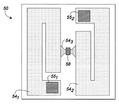
to Figs. 5(A) and (B), an electro-explosive device 50
according to a first embodiment of the invention
comprises a silicon wafer or thermally conductive but
electrically insulating substrate 52, such as alumina,
with layers of silicon dioxide 53 on the front and back
surfaces. The thin layers of silicon dioxide 53 provide
electrical insulation from the substrate 52 while
providing a low thermal resistance path from one side of
the substrate 52 to the other. Preferably, the substrate
52 has a low nom' n;3 1 resistivity and has a width of about
250 mils and the layers 53 of silicon dioxide are about
500 nanometers in thickness.
A thin layer 54 of aluminum is deposited on top of
the silicon dioxide layer 53 and is selectively etched
away to produce a serpentine pattern. The layer 54 of
aluminum forms a first path 5411 a second path 542, and a
bowtie area 543, with the bowtie area 543 interconnecting
the first and second paths 541 and 542. The first and
second paths 541 and 542 preferably have a width of about
50 mils and the bowtie area 543 preferably has ~;men~ions
of about 5 mils by 10 mils at the th;nnest portion of the
area 543.
A layer 58 of zirconium is selectively deposited
over the bowtie region 543. The layer 58 of zirconium is
not limited to the shape shown but may cover a greater or
~t 83488
- 16 -
lesser area of the bowtie area 543. For instance, the
layer 58 of zirconium may extend across almost the entire
length of the bowtie area 543 from the first path 541 to
the second path 542. The zirconium layer 58 is preferably
about 1 ~m in thickness.
Layers 551 and 552 of titanium/nickel/gold (Ti/Ni/Au)
are selectively deposited over the ends of the aluminum
paths 54~ and 542, respectively. The titanium in the
layers 55 provides adhesion to the aluminum layer 54, the
nickel provides a solderable contact, and the gold
protects the nickel surface from oxidation. Contact to
the Ti/Ni/Au layers 551 and 552 on the all~m;nllm paths 541
and 542 may be accomplished in any suitable manner, such
as wire bonding, solder reflow, or conductive epoxy. The
Ti/Ni/Au layers 55 are preferably about 0.6 ,um in
thickness.
With reference to Figs. 5(B) and 6, an initiator 60
is formed by depositing a layer 59 of
titanium/nickel/gold (Ti/Ni/Au) on the backside of the
substrate 52 over the silicon dioxide layer 53 and then
attaching the Ti/Ni/Au layer 59 to a header 62, which is
preferably formed from a ceramic or metal alloy, such as
Kovarm. The Ti/Ni/Au layer 59 is attached to the header
62 with a solder paste or conductive epoxy which is then
heated to permit the solder to flow or the epoxy to cure.
A conductive epoxy 64 is applied between pins 66 on the
header 62 and the Ti/Ni/Au layers 55 and cap 68 is placed
on the header 62 to form an enclosure filled with a gas
generating mix or pyrotechnic mix 69.
~1 83~8~
- 17 -
In operation, a firing signal supplied to the
initiator 60 is routed through the pins 66, through the
conductive epoxy 64, and to the Ti/Ni/Au layers 55. The
firing signal produces a current which travels along one
of the two paths 541 or 542, through the bowtie area 543
and then through the other of the two paths 541 or 542.
The resistance of the alllm;nllm layer 54 is essentially
comprised of three resistors in series, with the paths 54
and 542 each having a resistance of R1 and the bowtie area
543 having a resistance of Rb.
In general, the resistance R of the alllm;n~lm layer
54 can be calculated from the following equation:
R = P(hW)
EQ. l,
where p is the bulk resistivity of the material, L is the
length of the metal trace, h is the height or thickness,
and w is the width.
With the initiator 60, the electrical impedance
presented to a signal applied to the pins 66 is purely
resistive in nature and is approximately equal to the sum
of 2R1 and Rb. The aluminum layer 54 defines a resistive
divider network with the resistors R1 and Rb and the
signal that is actually being applied to the bowtie area
54b is attenuated by an amount equal to the ration of
Rb/2R~. The
21 8348~
- 18 -
attenuation A of the applied signal can be simplified as:
A = (Lb/wb)
(2Lp/wp)
EQ. 2,
where Lb and wb are the length and width of the bowtie
area 543 and Lp and wp are the length and width of either
path 541 or 542
As is apparent from Equation 2, the attenuation A of
a signal is a constant value at low levels of an input
signal and is determined only by the relative length to
width ratios of the resistors R1 and Rb. The alnm;nllm
layer 54 is preferably designed to achieve an attenuation
A of about 1/20, which is about -26 dB. It will be
apparent to those skilled in the art, however, that the
amount of attenuation A is not limited to this exact
value but that other values of attenuation A can be
obtained by simply varying the geometries of the aluminum
layer 54.
Due to the attenuation A obtained by the resistive
network of resistors Rl and resistor Rb, the majority of
electrical power supplied to the initiator 60 is
converted to heat by ohmically heating the two resistors
Rl. The resistors R~ possess a large surface to volume
ratio so as to provide a large surface area for the
conduction of heat from the resistors R1, through the top
layer of silicon dioxide 53, into the thermally
conductive silicon substrate 52, and to the header 62.
The initiator 60 may additionally have a heat sink to
2 1 834~
- 19 -
further dissipate heat away from the bowtie area 543 and
thus away from the zirconium layer 58.
The EED 50 is therefore insensitive to coupled RF
power. Due to the resistive network defined by the
resistors R1 and Rb, the coupled RF power is attenuated
whereby the bowtie 543 receives only a fraction of the
energy. Furthermore, because the heat from the resistors
R1 as well as the resistor R3 is routed away from the
bowtie area 543, the bowtie area 543 and the zirconium
layer 58 remain relatively cool. Consequently, coupled
RF power can be dissipated into heat without accidentally
firing the EED 50.
The EED 50 is also insensitive to an electrostatic
discharge (ESD) since the time period of the discharge is
too short to heat the bowtie 543 any appreciable amount.
A pulsed signal from an ESD will have the vast majority
of the energy coupled to the large resistors R~ with the
heat generated by the resistors R1 being safely dissipated
through the header 62.
In order to fire the EED 50, a current having a
sufficiently long duration is passed through the
resistors R1 and Rb to increase the temperatures of the
resistor Rb. The resistors Rl and Rb have a positive
temperature coefficient so that the resistances will
increase with the temperature of the aluminum layer 54.
Because the bowtie area 543 is much smaller than the
serpentine resistors R1, the firing signal will cause the
bowtie area 543 to heat up much faster than the other
areas 541 and 542. As the temperature of the bowtie area
21 ~3488
-
- 20 -
543 increases, the resistance of resistor Rb will increase
by upwards of two orders of magnitude and will eventually
become larger than the resistors R1. As a result, the
bowtie area 543 will receive most of the electrical power
from the firing signal and will rapidly heat and
evaporate along with the zirconium layer 58 in a plasma.
The plasma condenses on a small area of nearby
pyrotechnic compound 69 causing it to heat. Once a
critical volume of the pyrotechnic material 69 reaches
its ignition point, the entire pyrotechnic compound 69
ignites. The zirconium layer 58 assists in the ignition
of the pyrotechnic compound 69 by increasing the mass of
material in the bowtie area 543 which will change from
solid to plasma. With a larger mass, a greater amount of
material is available to condense on the pyrotechnic
powder 69 and a greater amount of thermal energy can be
transferred.
As described above, when the temperature of the
bowtie area 543 increases, the resistance of resistor Rb
will increase. Once the bowtie area 543 becomes molten,
the resistance of resistor Rb, which has a geometry
selected according to the resistance of an initiation
system, matches the parasitic resistance of the
initiation system supplying the firing signal. Thus, by
matching the increased resistance of the alllm;nllm layer
54 to the initiation system, the m~3~C; mllm amount of power
can be transferred to the bowtie area 543.
The pyrotechnic compound 69 is a combination of
powdered zirconium and potassium perchlorate. With some
2 i g 3 4 88
- 21 -
previous EED's, a layer of conductive or semiconductor
material is heated into a plasma state and the plasma
condenses on the pyrotechnic compound in order to ignite
the EED.
With the invention, on the other hand, the zirconium
layer 58 is converted into the plasma state in
conjunction with the bowtie area 543. The vaporous
zirconium aides in the ignition by directly reacting with
the potassium perchlorate. The EED according to the
invention is consequently a more efficient ignition
mechanism since an element of the pyrotechnic mix 69 is
vaporized with the metal. By using zirconium which burns
upon ignition, an EED of the invention eliminates the
need for a primary explosive, such as lead azide. As a
result, the EED of the invention can be surrounded by a
lower strength and lower cost steel mesh.
An EED according to the invention was subjected to a
12 MHz sinusoidal RF signal which coupled approximately
1.5 W of real power to the EED structure. The EED did
not have any additional heat sink and no attempt was made
to increase the airflow over the EED structure. After
the EED was subjected to this signal for approximately 15
minutes, the heat was effectively dissipated from the EED
structure whereby the EED structure could be easily held
by hand. Also, a visual inspection of the serpentine
resistor and bowtie did not reveal any damage. The EED
structure was subjected to additional frequencies with
similar results. The EED according to the invention is
therefore insensitive to real RF power.
21 8348~
- 22 -
An EED according to the invention was also subjected
to an ESD. The ESD consisted of current pulses of
approximately 30 amps for a variety of time periods up to
1 ~sec. A visual inspection of the EED structure after
the ESD pulses did not reveal any damage. Due to the
geometries of the serpentine resistors and bowtie, the
ESD is primarily coupled to the serpentine resistors and
away from the bowtie with most of the energy being
dissipated by the serpentine resistors. The EED~s were
also repetitively pulsed with the result that no adverse
effects had occurred.
To ensure that the EED's according to the invention
would fire with a proper firing signal, EED's were
connected to a 480 ~F electrolytic capacitor which had
been charged to 8 V. The capacitor was switched in
series with the EED structure by a metal-oxide-
semiconductor transistor (MOSFET). A variety of EED's
were fired with this test setup after RF testing and
after ESD testing to verify the functionality of the
EED's. As expected, all of the EED's were ignited with a
range of 1.0 mJ to 3.0 mJ total energy being absorbed
from the electrolytic capacitor.
With the invention, only a small portion of the
available 15 mJ of energy is needed to fire the EED. An
EED according to the invention can therefore be fired
with low energies. The low energy firing capability of
the invention is especially advantageous when an
initiator firing circuit has a high parasitic resistance,
such as in an automobile airbag system. The actuation of
21 834~
.
- 23 -
numerous EED's from a single low energy source is also
much more feasible with a low firing energy device.
Thus, a single low energy source may be able to activate
the numerous airbags which will likely be installed in
future designs of automobiles.
An EED according to the invention is a relatively
simple integrated structure which can be produced with
extremely small geometries. The EED provides a constant
attenuation of stray RF and spurious signals across the
entire frequency spectrum and can also safely and
repetitively dissipate the energy of a typical ESD event
in both pin-to-pin and pin-to-case modes.
The invention is not limited to the pyrotechnic
compound of zirconium and potassium perchlorate but
rather may employ other pyrotechnic compounds. For
instance, the pyrotechnic compounds may comprise any
suitable combination of a powdered metal with a suitable
oxidizer, such as TiHl68KClO4 or other mixtures such as
boron and potassium nitrate BKNO3. If potassium nitrate
BKNO3 were used as the pyrotechnic compound, a coating of
boron could be applied over the bowtie area 543 to enhance
the ignition process. As will be apparent to those
skilled in the art, by matching the hot vapor phase of
the plasma to the pyrotechnic compound, a variety of
materials can be used to coat the bowtie area 543to
enhance the ignition process.
The material coating the bowtie area 543 need not be
in electrical contact with the bowtie area 543 but may
instead be electrically isolated from the bowtie area 543.
21 83488
-
- 24 -
The material is primarily heated by conductive heat
transfer from the bowtie area 543 and is not caused by
Joule heating, which occurs when a current flows through
the material. Thus, one or more electrically insulating
but thermally conductive materials can be placed between
the bowtie area 543 and the coating material.
The invention is also not limited to the serpentine
resistors and/or the bowtie area being formed from
aluminum but rather may be fabricated from a variety of
different conductive materials such as printed conductive
traces or conductive epoxy. Further, the ~;men~ions of
the serpentine resistors and bowtie area may be varied to
obtain different magnitudes of attenuation. Also, an EED
according to the invention may have a bowtie area without
any type of coating material whereby only the bowtie area
would evaporate in a plasma.
In a second embodiment of the invention, as shown in
Figs. 7(A) and (B), an EED 70 comprises a silicon wafer
or a thermally conductive but electrically insulating
substrate 72, such as alumina, which has layers 74 of
silicon dioxide grown on the front and back surfaces.
The silicon dioxide layers 74 electrically insulate the
substrate 72 while providing a low thermal path of
resistance across the front and back surfaces of the
substrate 72. Preferably, the substrate has a nom;n~l
low resistivity and is about 50 mils in width and length
and the silicon dioxide layers 74 are approximately 500
n~nometerS in thickness.
2 1 8348~
- 25 -
A layer 76 of titanium is vapor deposited onto the
front surface followed by a layer 78 of zirconium. The
titanium layer 76 is preferably about 0.1 ~m in thickness
and the zirconium layer 78 is about 1 ~m in thickness.
The zirconium/titanium layer 78 is then selectively
etched away to form a bowtie pattern having a central
bridge portion with ~limPn~ionS of about 1.5 mils by 1.5
mils.
A layer 77 of titanium/nickel/gold (Ti/Ni/Au) is
deposited over the back layer 74 of silicon dioxide and
Ti/Ni/AU layers 791 and 792 are also deposited over the
ends of the bowtie shaped zirconium layer 78 to form
contact pads. AS with the embodiment of Figs. 5 (A) and
(B), the EED 70 may be attached to the header 62 with a
conductive epoxy connecting the header pins 66 to the
Ti/Ni/AU contact pads 79~ and 792, or with other
interconnect schemes, including wirebonding, etc.
The resistance of the EED 70 is comprised of three
resistors in series, with R"",d being the resistance
through the Ti/Ni/Au layers 79 to either end of the
bowtie-shaped zirconium layer 78 and Rbo~, being the
resistance of the bowtie-shaped zirconium layer 78. In
the preferred embodiment, R""d is approximately 10 to 20
ohms while Rbo~" is only about 0.3 ohms. The resistance of
the bowtie-shaped zirconium layer 78 is determined in
accordance with Equation 1.
The electrical impedance presented to a signal
applied across the Ti/Ni/Au contacts 79 is purely
resistive in nature and is equal to the sum of 2R,~",d and
2 1 8348&
- 26 -
Rb~. The signals reaching the zirconium layer 78 are
attenuated by an amount A equal to Rb~/2R~d, which can be
simplified as:
A = (Lbow/Wbow)
2Rland
EQ. 3,
which is a constant value at low levels of input signal
and is determined onIy by the length Lb~ and width Wb~ of
the bowtie-shaped zirconium layer 78 and the resistances
R~d. Although the attenuation A is preferably about
1/20, or -26 dB, any practical value of attenuation A may
be achieved by simply varying the geometry of the
zirconium layer 78.
With low levels of input signals, the resistances
R~d, which are about 10 to 20 ohms, have a much larger
surface to volume ratio than the resistance Rb~. Thus,
at these levels, the resistances R~d receive most of the
energy from the input signals and convert the energy into
heat. The Ti/Ni/Au contacts 79 present a large surface
area for the conduction of heat through the top silicon
dioxide layer 74, through the thermally conductive
substrate 72 and to the header 62. As a result, at low
levels of input signal, the zirconium-shaped bowtie 78
dissipates only a fraction of the heat and remains
relatively cool. Thus, the EED 70 can remain insensitive
to any RF power or ESD which is coupled to the EED 70.
The EED 70 is ignited by supplying a firing signal
which has a relatively high intensity. The resistances
2 1 834~3
- 27 -
R~d comprise metal-oxide variable resistances which are
formed between the titanium layer in contacts 79 and an
oxide-phase layer formed on the zirconium layer 78. The
metal-oxide variable resistances R~d have a relatively
high resistance at lower voltages, such as 25 ohms with
an applied signal of 1 volt. With higher intensity
signals, the metal-oxide resistances R~d decrease
substantially and become small in comparison to the
resistance R~w. As a result, with a high intensity
firing signal, the resistance R~w will become the largest
resistance and will accordingly receive most of the
energy from the firing signal until the zirconium layer
78 evaporates in a plasma. The EED 70 may use the same
types of pyrotechnic compound as that of EED 50.
The EED 70 may additionally comprise a shunting
element connected in parallel between the Ti/Ni/Au
contacts 79. The shunting element has a low impedance at
RF frequencies and may comprise a ceramic capacitor, a
diode arrangement, or a low impedance fuse. Further, the
shunting element can be either a discrete component, a
combination of discrete components, or integrated
directly on the substrate 72.
An EED according to the second embodiment was found
to have an RF impedance of about 12 ohms. A 0.1 ~F
ceramic capacitor was placed across the EED as the
shunting element and the impedance was measured as 12/0
ohms at 10 kHz and 0.3 /-65 ohms at 10 MHz. As
expected, the impedance was primarily capacitive at
higher frequencies. The inductance of the leads
21 834~8
-- - 28 -
resonated at 4 MHZ and appeared inductive at higher
frequencies.
To conduct ESD testing, the EED of the second
embodiment was subjected to current pulses of
approximately 24 A for a variety of time periods up to a
fraction of a microsecond. An inspection of the EED
after the current pulses revealed that the EED was
unaffected. The EED' s were repetitively pulsed with no
adverse consequences.
To ensure that the EED' s of the second embodiment
would fire after ESD and RF testing, the EED' s were
connected to a 40 ~F electrolytic capacitor, which was
charged to 22 volts, and was switched in series with the
capacitor with a MOSFET transistor. A number of EED' S
were fired with this arrangement and absorbed from 1 mJ
to 3 mJ of total energy. The peak currents measured in
the EED were upwards of 16 amps for a duration of about 1
to 2 ~s. The EED' s 70 can therefore be ignited from only
a small fraction of the 10 mJ of available energy. The
20 EED' S could also be ignited with a 480 ~F capacitor
charged to only 10 volts.
With the second embodiment of the invention, non-
linear resistances R~d are placed in series with the
ignition element comprising the bowtie-shaped zirconium
layer 78. The invention can therefore protect the
ignition element from stray RF signals without the use of
a large ferrite sleeve and capacitor. Also, the ignition
element can be protected from an ESD without the use of
other elements, such as diodes.
~ 1 ~348~
- 29
Figs. 8(A) and (B) illustrate an example of a
shunting element 80 which may be placed in parallel
across an BED according to the invention, such as EED 50
or EED 70. In this example, the shunting element 80
comprises a low impedance fuse having a polished alumina
or silicon substrate 82. A thin layer 84 of titanium is
deposited onto the substrate 82 followed by a thicker
layer 86 of aluminum which is selectively etched away to
form a bowtie pattern. Preferably, the titanium layer 84
is about O.l ~m in thickness and the al~lm;nl]m layer is
about l.0 ,um in thickness and has ~l;m~nqions of about 1
mil by l mil at the bridge area of the bowtie pattern.
Also, the substrate has a width of about 60 mils. Two
layers of titanium/nickel/gold (Ti/Ni/Au) 881 and 882 are
deposited onto either end of the bowtie-shaped alnm;nl]m
layer 86 in order to form contacts for the shunting
element 80.
The contacts 88~ and 882 are connected in parallel to
the contacts on the EED, such as contacts 551 and 552 or
contacts 791 and 792. The resistance of the shunting
element 80 is approximately 0.2 ohms and therefore
provides a low impedance resistive path for shunting the
current away from the EED, thereby protecting the
igniter. The shunting element 80 also preferably
provides a low thermal impedance path from the aluminum
layer 86 to the substrate 82 as well as to a heat sink
which may be in thermal contact with the substrate 82.
With low levels of coupled RF energy and with an
ESD, the energy is routed through the shunting element 80
2 1 83~ g8
- 30 -
due to its low impedance. When a firing signal is
received, on the other hand, the firing signal has a
duration and energy level which are sufficient to open-
circuit the shunting element 80. Once the shunting
element 80 has been removed from the circuit, the firing
signal is coupled to the EED for igniting the EED. As
will be apparent to those skilled in the art, the amount
of energy needed to open-circuit the shunting element 80
can be adjusted by varying the geometry of the aluminum
layer 86.
A shunting element according to the invention is not
limited to the shunting element 80. For instance, a
shunting element may be integrated on the same substrate
as the EED or may be fabricated as a discrete component.
Further, a diode may additionally or alternatively be
used as the shunting element. A diode may be integrated
directly onto the silicon substrate of the EED. For
instance, a pn junction or a Schottky barrier both
possess a high enough junction capacitance per unit area
to effectively shunt stray RF signal. Furthermore, a
shunting element according to the invention may be used
in applications other than with an EED according to the
invention, such as with other EED's or in entirely
different types of circuits.
The foregoing description of the preferred
embodiments of the invention has been presented for
purposes of illustrating the features and principles
thereof. It is not intended to be exhaustive or to limit
the invention to the precise forms disclosed. Many
2 ~ ~i3~8
- 31 -
modifications and variations are possible in light of the
above teaching.
The embodiments were chosen and described in order
to explain the principles of the invention and their
practical application; various other possible embodiments
with various modifications as are suited to the
particular use are also contemplated and fall within the
scope of the present invention.