Note: Descriptions are shown in the official language in which they were submitted.
2 ~ 83324
TTTT,R OF THF! TT~TpFTT'T'T(7N
ELECTRON GENERATING DEVICE, IMAGE DISPLAY APPARATUS,
DRIVING CIRCUIT THEREFOR, AND DRIVING METHOD
RACK.GRQL_TD QF mr-T~ 'rnnrFrrrrnrT
The present invention relates to an electron
generating device including a multi-electron source
having a plurality of electron emitters wired in the
form of a matrix and a driving circuit for the
multi-electron source, an image display apparatus, a
driving circuit, and a driving method.
Conventionally, two types of devices, namely
thermionic and cold cathode devices, are known as
electron emitters. Examples of cold cathode devices are
field emission type electron emitters (to be referred to
as field emitters hereinafter), metal/insulator/metal
type electron emitters (to be referred to as MIM-type
electron emitters hereinafter), and surface-conduction
type electron emitters.
Itnown examples of the field emitters are described
in W.P. Dyke and W.W. Dolan, "Field Emission", Advance
in Electron Physics, 8, 89 (1956) and C.A. Spindt,
"Physical Properties of thin-film field emission
cathodes with molybdenum cones", J. Appl. Phys.,
47, 5248 (1976). Fig. 31 is a sectional view of a device
according to C.A. Spindt et al. Referring to Fig. 31,
- 1 -
,.
reference numeral 3010 denotes a substrate, 3011, an
emitter wring layer made of a conductive material; 3012,
an emitter cone; 3013, an insulating layer; and 3014, a
gate electrode. In this device, a proper voltage is
applied between the emitter cone 3012 and the gate
electrode 3014 to emit electrons from the distal end
portion of the emitter cone 3012.
A known example of the MIM-type electron emitters
is described in C.A. Mead, "Operation of Tunnel-Emission
Devices", J. Appl. Phys., 32,646 (1961). Fig. 32 is a
sectional view of an MIM-type electron emitter.
Referring to Fig. 32, reference numeral 3020 denotes a
substrate; 3021, a lower electrode made of a metal; 3022,
a thin insulating layer having a thickness of about 100
A; and 3023, ari upper electrode made of a metal and
having a thickness of about 80 to 300 Vii. In the MIM type,
a voltage is applied between the upper electrode 3023
and the lower electrode 3021 to emit electrons from the
surface of the upper electrode 3023.
A known example of the surface-conduction type
electron emitters is described in, e.g., M.I. Elinson,
"Radio Eng. Electron Phys., 10, 1290 (1965) and other -
examples to be described later.
The surface-conduction type electron emitter
utilizes the phenomenon that electron emission takes
_ 2 -
t
place in a small-area thin film, formed on a substrate,
upon flowing a current parallel to the film surface. The
surface-conduction type electron emitter includes
electron emitters using an Au thin film (G. Dittmer,
"Thin Solid Films°, 9,317 (1972)), an Inzp3/SnO~ thin film
(M. Hartwell and C.G. Fonstad, "IEEE Trans. ED Conf.",
519 (1975)), a carbon thin film (Hisashi Araki et al.,
"Vacuum", vol. 26, No. 1, p. 22 (1983), and the like, in
addition to an SnOz thin film according to Elinson
mentioned above.
Fig. 30 is a plan view of the surface-conduction
type electron emitter according to M. Hartwell et al. as
a typical example of the structures of these
surface-conduction type electron emitters. Referring to
Fig. 30, reference numeral 3001 denotes a substrate; and
3004, a conductive thin film made of a metal oxide
formed by spattering. This conductive thin film 3004 has
an H-shaped pattern, as shown in Fig. 30. An
electron-emitting portion 3005 is formed by performing
an energization process (referred to as an energization
forming process to be described later) with respect to
the conductive thin film 3004. Referring to Fig. 30, an
interval L is set to 0.5 to 1 mm, and a width W is set
to 0.1 mm. For the sake of illustrative convenience, the
electron-emitting portion 3005 is shown in a rectangular
- 3 -
,,
~~83824
shape at the center of the conductive thin film 3004.
However, this does not exactly show the actual position
and shape of the electron-emitting portion.
In the above surface-conduction type electron
emitters according to M. Hartwell et al., typically the
electron-emitting portion 3005 is formed by performing
an energization process called the energization forming
process for the conductive thin film 3004 before
electron emission. According to the energization forming
process, energization is performed by applying a
constant DC voltage which increases at a very low rate
of, e.g., 1 V/min., across the two ends of the
conductive film 3004, so as to partially destroy or
deform the conductive film 3004, thereby forming the
electron-emitting portion 3005 with an electrically high
resistor. Note that the destroyed or deformed part of
the conductive thin film 3004 has a fissure. Upon
application of an appropriate voltage to the conductive
thin film 3004 after the energization forming process,
electron emission is performed near the fissure.
The above surface-conduction type electron emitters
are advantageous because they have a simple structure
and can be easily manufactured. For this reason, many
devices can be formed on a wide area. As disclosed in
Japanese Patent Laid-Open No. 64-31332 filed by the
- 4 -
present applicant, a method of arranging and driving a
lot of devices has been studied.
Regarding applications of surface-conduction type
electron emitters to, e.g., image forming apparatuses
such as an image display apparatus and an image
recording apparatus, charged beam sources and the like
have been studied.
As an application to image display apparatuses, in
particular, as disclosed in the U.S. Patent
No. 5,066,883 and Japanese Patent Laid-Open No. 2-257551
filed by the present applicant, an forage display
apparatus using the combination of a surface-conduction
type electron emitter and a phosphor which emits light
upon irradiation of an electron beam has been studied.
This type of image display apparatus is expected to have
more excellent characteristic than other conventional
image display apparatuses. For example, in comparison
with recent popular liquid crystal display apparatuses,
the above display apparatus is superior in that it does
not require a backlight since it is of a self-emission
type and that it has a wide view angle.
The present inventors have experimented on surface-
conduction type electron emitters made of various
materials, manufactured by various methods, and having
various structures as well as the one described above_
- 5 -
The present inventors have also studied multi-electron
sources each constituted by an array of many surface-
conduction type electron emitters, and image display
apparatuses using the multi-electron sources.
The present inventors have experimentally
manufactured a multi-electron source formed by an
electrical wiring method like the one shown in Fig. 33.
In this multi-electron source, a large number of
surface-conduction type electron emitters are -
two-dimensionally arrayed and wired in the form of a -
matrix, as shown in Fig. 33.
Referring to Fig. 33, reference numeral 4001
denotes a surface-conduction type electron emitter which
is schematically shown; 4002, a row wiring layer; and
4003, a column wiring layer. In reality, the row and
column wiring layers 4004 and 4005 have finite electric
resistors. However, Fig. 33 shows these resistors as
wiring resistors 4004 and 4005. The above wiring method
will be referred to as simple matrix wiring.
For the sake of illustrative convenience, Fig. 33
shows a 6 x 6 matrix. However, the size of a matrix is
not limited to this. For example, in a multi-electron
source for an image display apparatus, a sufficient
number of emitters for a desired image display operation
are arrayed and wired. -
- 6 -
,~ ~ 8~ 8.~~
In the multi-electron source having the surface-
conduction type electron emitters wired in the form of a
simple matrix, in order to output desired electron beams,
proper electrical signals are applied to the row and
column wiring layers 4002 and 4003. For example, in
order to drive the surface-conduction type electron
emitters on an arbitrary row in the matrix, a selection
voltage Vs is applied to the row wiring layer 4002 on a
selected row, and at the same time, a non-selection
voltage Vns is applied to each row wiring layer 4002 on
the non-selected rows. A drive voltage Ve,is applied to
each column wiring layer 4003 in synchronism with the
non-selection voltage Vs. According to this method,
ignoring voltage drops caused by wiring resistors 4004
and 4005, a voltage Ve - Vs is applied to each surface-
conduction type electron emitter on the selected row,
whereas a voltage Ve - Vns is applied to each surface-
conduction type electron emitter on the non-selected
rows. If, therefore, the voltages Ve, Vs, and Vns are
set to proper voltages, an electron beam having a
desired intensity should be output from each surface-
conduction type electron emitter on only a selected row.
In addition, if different drive voltages Ve are applied
to the respective column wiring layers, electron beams
having different intensities should be output from the
respective emitters on a selected row. Since the
response speed of each surface-conduction type electron
emitter is high, the length of time that an electron
beam is kept output should be changed if the length of
time that the drive voltage Ve is kept applied is
changed.
Various applications of such a multi-electron
source having surface-conduction type electron emitters
wired in the form of a simple matrix have therefore been
studied. For example, this electron source is expected
to be used in an image display apparatus which applies
voltage signals in accordance with image information.
In practice, however, when the multi-electron
source to which a voltage source is connected is driven
by the above voltage application method, voltage drops
occur across wiring resistors, resulting in variations
in voltages effectively applied to the respective
surface-conduction type electron emitters. The first
cause for variations in voltages applied to the
respective emitters is that the respective surface-
conduction type electron emitters in the simple matrix -
wiring structure have different wiring lengths (i.e.,
different wiring resistors).
The second cause is that voltage drops caused by
the wiring resistors 4004 in the respective row wiring
- g -
layers vary. This is because a current branches from the
row wiring layer on a selected row to the respective
surface-conduction type electron emitters connected
thereto so as to cause nonuniform currents to flow in
the respective wiring resistors 4004.
The third cause is that the magnitude of a voltage
drop caused by a wiring resistor changes depending on
the driving pattern (the image pattern to be displayed
in the case of an image display apparatus). This is
because a current flowing in a wiring resistor changes
depending on the driving pattern.
If the voltages applied to the respective surface-
conduction type electron emitters vary due to the above
causes, the intensity of an electron beam output fram
each surface-conduction type electron emitter deviates
from a desired value, posing a problem in practical use.
For example,-when the electron source is applied to an
image display apparatus, the luminance of the displayed
image becomes nonuniform, or variations in luminance -
occur depending on the display image pattern. In
addition, variations in voltage tend to increase with an
increase in the size of a simple matrix. 'this tendency
is a factor that limits the number of pixels in an image -
display apparatus.
In the process of studying such techniques in
- 9 -
2183824
consideration of the above problems, the present
inventors have already experimented on a driving method
different from the above voltage application method. In
this method, when a multi-electron source having
surface-conduction type electron emitters wired in the
form of a simple matrix is to be driven, a current
source for supplying currents required to output desired
electron beams is connected to the column wiring layers,
instead of connecting a voltage source for applying the
drive voltage Ve to each column wiring layer, so as to
drive the multi-electron source. This method was devised
in consideration of the strong correlation between the
current (to be referred to as an emitter current If
hereinafter) flowing in each surface-conduction type
electron emitter and the electron beam (to be referred
to as an emission current Ie hereinafter) emitted from
each emitter. In the method, the magnitude of the
emission current Ie is controlled by limiting the -
magnitude of the emitter current If.
That is, the magnitude of the emitter current If to
be supplied to each surface-conduction type electron
emitter is determined by referring to the (emitter
current If) to (emission current Ie) characteristics of
each surface-conduction type electron emitter, and the
emitter current If is supplied from the current source
- 10 -
,.
connected to each column wiring layer. More specifically,
a driving circuit may be constituted by a combination of
electric circuits such as a memory storing the (emitter
current If) to (emission current Ie) characteristics, an
arithmetic unit for determining the emitter current If
to be supplied, and a controlled current source. As the
controlled current source, a circuit form for
temporarily converting the magnitude of the emitter
current If to be supplied into a voltage signal, and -
converting the signal into a current using a
voltage/current conversion circuit may be used. This
method is less susceptible to voltage drops caused by
wiring resistors than the above method of driving the
multi-electron source using the voltage source connected
to each column wiring layer. It was found therefore that
this method could reduce variations in the intensity of
an electron beam to be output.
However, the following problem is posed in the
method of driving the electron source using the current
source connected thereto. This problem will be described
with reference to Fig. 34. Fig. 34 shows a case wherein
the multi-electron source in Fig. 33 is driven by
current sources. A selection potential Vs = -7 V is
applied to a row wiring layer D,~ of row wiring layers
4002,. and a non-selection potential Vns = 0 V is applied
- 11 -
.. ~ 2 ~ 83824
to the remaining row wiring layers 4002, i.e., row
wiring layers D,Q to Due. Column wiring layers 4003, i.e.,
column wiring layers D1,, to Due, are connected to constant
current sources 4006. With this arrangement, the
emitters on the row wiring layer to which the selection
potential has been applied are driven by the constant
currents. In this case, the set value of each constant
current is set to a magnitude at which each emitter
emits electrons. With this setting, when a current is
output from each current source, a set emitter current
If flows in each emitter on the row to which the
selection potential has been applied. As a result, each
emitter emits electrons.
At this time, control must be performed to inhibit
some emitter from emitting electrons (turn-off
operation) depending on an actual video signal. Consider,
for example, a case wherein no electrons are to be
emitted from the emitter at the intersection of the row
wiring layer D,a and the column wiring layer Due, of the
emitters on the row wiring layer D,a to which the
selection potential Vs has been applied, as shown in
Fig. 34. In this case, the constant current source
connected to the column wiring layer Dys is set in a
state in which no current is output. This state in which
the output current from the constant current source is
- 12 -
"
set to 0 is equivalent to a state in which the output
impedance of the constant current source becomes
infinite. As a result, the column wiring layer D~ is
set in a high-impedance state. When a row or column
wiring layer of a simple matrix is set in the
high-impedance, the following problems are posed.
(1) A wiring layer in the high-impedance state
which is not determined by a current source output has a
potential determined by the influences of other driven
emitters or a driving pattern. Eor this reason, even if
a current source connected to a column is controlled to
inhibit an emitter from emitting electrons, a potential
to be applied to this emitter on the column cannot be
determined. That is, an emitter on a wiring layer-in the
high-impedance state may emit electrons regardless of a
video signal (abnormal turn-on operation) depending on
the influences of other driven emitters, a driving
pattern, and the state of a selection/non-selection
voltage. .
(2) In an image display apparatus using a
combination of a surface-conduction type electron
emitter and a phosphor which emits light upon
irradiation of an electron beam, the orbit of an
electron beam is influenced by a high voltage applied to
the phosphor side, and the potentials of adjacent row
- 13 -
.. ~ ~i$~8.'~
and column wiring layers. If, therefore, there is a
wiring layer potential of a high impedance, the electron
orbits of--emission electrons from adjacent lines are
influenced. In, for example, a color display apparatus,
an electron beam shift may cause color misregistration.
It is an object of the present invention to provide
a driving circuit designed to perform a current driving
operation, which is advantageous in overcoming the
problem of voltage drops, without causing any abnormal
turn-on operation and electron orbit shift, an electron
generating device using the same, an image display
apparatus, and a driving method therefor.
In order to achieve the above object, the present
inventors have made efforts to obtain the following.
There is provided an electron generating device
comprising a multi-electron source having a plurality of
electron emitters wired in the form of a matrix through
a plurality of data wiring layers and a plurality of
scanning wiring layers, and a driving circuit for
driving the multi-electron source, characterized in that
a constant current output unit for outputting a constant
current and a constant voltage output unit for
outputting a constant voltage are connected to the data
wiring layers via a switch. The present invention
- 14 -
,.
includes an image display apparatus using the electron
generating device. According to the present invention,
there is provided an image display apparatus comprising
a multi-electron source having a plurality of electron
emitters wired in the form of a matrix through a
plurality of data wiring layers and a plurality of
scanning wiring layers, a driving circuit for driving
the multi-electron source, and a phosphor which is
excited to emit light upon irradiation of electrons,
characterized in that a constant current output unit for
outputting a constant current and a constant voltage
output unit for outputting a constant voltage are
connected to the data wiring layers via a switch. The
present invention includes a driving circuit for the
electron generating device and the image display
apparatus. According to the present invention, there is
provided a driving circuit for driving a multi-electron -
source having a plurality of electron emitters wired in
the form of a matrix through a plurality of data wiring
layers and a plurality of scanning wiring layers,
characterized in that a constant current output unit for
outputting a constant current and a constant voltage
output unit for outputting a constant voltage are
connected to the data wiring layers via a switch.
Zn the present invention, the constant current
- 15 -
1
,,
output from the constant current output unit is
preferably an emitter current to be flowed to the
electron emitter to obtain a desired emission current,
and the constant voltage output from the constant
voltage output unit is preferably a voltage which is set
such that a difference between the constant voltage and
a scanning voltage applied to the scanning wiring layer
is smaller than a value of an electron emission
threshold voltage of the electron emitter. The switch
preferably switches connection between the constant
current output unit and the data wiring layer and
connection between the constant voltage output unit and -
the data wiring layer. The switch preferably comprises
switches equal in number to the data wiring layers. The
switch preferably comprises a transistor. The transistor
may be a bipolar transistor or enhancement type MOS
transistor. If the transistor is a bipolar transistor,
the collector or emitter is preferably grounded. If the
transistor is an enhancement type MOS transistor, the
drain or source is preferably grounded. The driving
circuit preferably includes a pulse-width modulation
circuit for performing a switching operation of the
switch. The constant voltage output unit preferably
comprises a GND wiring layer. The switch may include a
diode, 44hen the switch is a diode, the circuit
- 16 -
,.
preferably includes a timing generation circuit for
performing a switching operation of the switch. The
constant-current output unit preferably comprises a V/I
converter. The switch preferably connects the data
wiring layer to the constant voltage output unit when a
value of a luminance signal is smaller than a value of a
reference signal, and connects the data wiring layer to
the constant current output unit when the value of the
luminance signal is not less than the value of the
reference signal. In addition, the switch preferably
connects the data wiring layer connected to an electron
source whose electron emission amount is to be 0 to the
constant voltage output unit, and connects the data
wiring layer connected to an electron source whose
electron emission amount is to be a value other than 0
to the constant current output unit.
The present invention also a driving method for an
electron generating device and an image display
apparatus. According to the present invention, there is
provided a driving method for an electron generating
device including a multi-electron source having a
plurality of electron emitters wired in the form of a -
matrix through a plurality of data wiring layers and a
plurality of scanning wiring layers, and a driving
circuit for outputting a luminance signal to the
- 17 -
t
.. ~ ~ i 8382
plurality of data wiring layers of the multi-electron
source, characterized in that the luminance signal is
output to the data wiring layers while a constant
current signal and a constant voltage are switched.
In addition, according to the present invention,
there is provided a driving method for an image display
apparatus including a multi-electron source having a
plurality of electron emitters wired in the form of a
matrix through a plurality of data wiring layers and a
plurality of scanning wiring layers, a driving circuit
for outputting a luminancesignal to the plurality of
data wiring layers of the multi-electron source, and a
phosphor plate which is excited to emit light upon
irradiation of electrons, characterized in that the
luminance signal is output to the data wiring layers
while a constant current signal and a constant voltage
are switched. The constant current signal is preferably
output from a V/I converter. The constant voltage is
preferably GND. The constant current signal and the
constant voltage may be switched in accordance with an
output signal from a pulse-width modulation circuit or a
timing generation circuit. The timing ,generation circuit
preferably outputs the constant current signal to the
data wiring layer during a video display period, and
outputs a pulse for setting the data wiring to the
- 18 -
z~~'u~~~~~
constant voltage during a blanking period.
According to the present invention, in a display
apparatus in which a plurality of electron emitters are
wired in the form of a matrix, and current sources for
supplying currents required to output- desired electron
beams are connected to the.emitters to drive them, the
following effects can be obtained:
(1) Even if an output current from a
constant-current source becomes 0, an abnormal turn-on
operation of each emitter on the high-impedance wiring
layer can be prevented.
(2) Even if an output current from a
constant-current source becomes 0, the adverse effect of
the high-impedance state on the orbits of electrons from
the adjacent lines can be eliminated.
With these effects, an image which is very stable
with respect to an original video signal can be
displayed throughout the display screen.
Other features and advantages of the present
invention will be apparent from the following
description taken in conjunction with the accompanying
drawings, in which like reference characters designate
the same or similar parts throughout the figures
thereof.
- 19 -
,.
BRIEF DESCRTpmTON OF TF~ DRAWTNCR
Fig. 1 is a block diagram showing a driving circuit
of the present invention;
Fig. 2 is a block diagram showing the flow of a
video signal in Example 1 of the present invention;
Fig. 3 is a circuit diagram showing switches and
constant current-current circuits in Example 1;
Figs. 4A to 4G are timing charts associated with
column wiring layer 1 in Example 1;
Fig. 5 is a perspective view showing a display
panel;
Figs. 6A and 6B are views each showing the
arrangement of phosphors on a faceplate;
Figs. 7A and 7B are plan and sectional views,
I5 respectively, showing a flat surface-conduction type
electron emitter;
Figs. 8A to 8E are sectional views showing a
manufacturing process of a flat surface-conduction type
electron emitter;
Fig. 9 is a timing chart showing energization
forming voltages;
Figs. 10A and 10B are timing charts activation
voltages and emission currents;
Fig. 11 is a sectional ugh showing a stepped
surface-conduction type electron emitter;
_ 20 _
t
"
Figs. 12A to 12F are sectional views showing a
manufacturing process of a stepped surface-conduction
type electron emitter;
Fig. 13 is a graph showing voltage/current
characteristics of a surface-conduction type electron
emitter;
Fig. 14 is a plan view showing a multi-electron
substrate;
Fig. 15 is a partial sectional view showing a
multi-electron substrate;
Fig. 16 is a circuit diagram showing switches and
constant-current circuits in Example 2 of the present
invention;
Figs. 17A to 17G are timing charts associated with
column wiring layer 1 in Example 2;
Fig. 18 is a block diagram showing the flow of a
video signal in Example 3 of the present invention;
Fig. 19 is a circuit diagram showing switches and
constant-current circuits in Example 3;
Figs. 20A to 20G are timing charts associated with
column wiring layer 1 in Example 3;
Fig. 21 is a view showing a multi-electron source
and a driving circuit according to Example 4 of the
present invention;
Fig. 22 is a block diagram showing the driving
- 21 -
,.
circuit according to Example 4;
Fig. 23 is a circuit diagram showing a push-pull
structure in a scanning circuit;
Fig. 24 is a timing chart for the circuit in
Fig. 23;
Fig. 25 is a block diagram showing a V/I conversion
circuit;
Fig. 26 is a circuit diagram showing a V/I
conversion circuit in Example 4;
Figs. 27A to 27C are timing charts of Example 4;
Figs. 28A to 28C are perspective views showing
lateral-type field emitters;
Fig. 29 is a view showing a multi-electron source
using lateral-type field emitters;
I5 Fig. 30 is a plan view showing the surface
conduction type electron. emitter disclosed by
M. Hartwell;
Fig. 31 is a sectional view showing a conventional
Spindt-type field emitter;
Fig. 32 is a sectional view showing a conventional
MIM-type electron emitter;
Fig. 33 is a view showing a simple matrix wiring
structure; and
Fig. 34 is a view showing a simple matrix wiring
structure to be current-driven.
- 22 _
CA 02183824 1999-09-03
~7ETAILED DESCRIPTION OF THE PREFERRED EMBODIMENTS
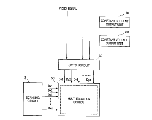
Fig. 1 shows the concept of the present invention.
Referring to Fig. 1, reference numeral 10 denotes a
constant current output unit; 20, a constant voltage
output unit; 30, a switch; and 50, a multi-electron
source. Reference symbols DY1, Dye, . . . , Dm and Due, D,~, . . . ,
D~" respectively denote the terminals of the data and
scanning wiring layers of the multi-electron source 50.
The multi-electron source 50 is a portion for emitting
electrons in multiple directions. If phosphors which are
excited to emit light upon irradiation of electrons are
arranged above the multi-electron source 50, a display
panel is obtained. A scanning circuit 2 is a circuit for
sequentially outputting selection signals to scanning
wiring layers to line sequentially driving the
multi-electron source 50. The constant current output
unit 10 is a portion for outputting a constant current
to the switch 30. The constant voltage output unit 20 is
a portion for outputting a constant voltage to the
switch 30_ The switch 30 switches and outputs signals
from the constant current output unit 10 and the
constant voltage output unit 20 to the terminals DY1 to
,~, of the data wiring layers of the multi-electron source 50
accordance with a video signal_ The ,arrangement shown in
Fig_tl is based on the premise that column and row
- 23 -
wiring layers are respectively used as data and scanning
wiring layers, and line sequential driving is performed
to select the rows one by one. However, column and row
wiring layers may be used as scanning and data wiring
layers, respectively, to perform line sequential driving
so as to select the columns one by one.
As a circuit, the constant current output unit 10
may include only one V/I converter to serially output a
constant current to the switch 30. Alternatively, the
constant current output unit 10 may use wiring layers
equal in number (n) to the wiring layers connected to
the multi-electron source 50 to parallely output
constant currents to the switch 30. The parallel
constant currents may be different constant currents in
consideration of reactive currents in the respective
data wiring layers. As the V/I converter, a current
mirror circuit, a Darlington connection circuit, a
constant-current diode, or the like is available. The
value of each constant current can be changed by
changing the voltage (V) input to the V/I converter or
the resistance of the resistor of the V/I converter.
As the electron sources constituting the
multi-electron source 50, cold cathode devices are
preferably used. Of the cold cathode devices, surface-
conduqtion type electron emitters are more preferable. A
- 24 -
x
dot matrix type image display apparatus can be
manufactured by mounting a phosphor plate, which emits
light upon irradiation of electrons, above the
multi-electron source 50. Therefore, an electron
generating device and an image display apparatus which
use the driving circuit of the present invention fall
within the scope of the present invention. The image
display apparatus may be a color or monochrome image
display apparatus. In the case of the color image
display apparatus, the phosphor plate includes red (R),
blue (B), and green (G) pixels, and the multi-electron
source 50 also includes electron sources for the red
pixels, electron sources for the blue pixels, and
electron sources for the green pixels. The
multi-electron source can expose a resist on a
semiconductor substrate or can be used as an excitation
source for image formation in a optical printer.
[Example 1]
(Driving Method and Correction Method)
The driving and correction methods for the image
display apparatus, which are the main features of the
present invention, will be described. The arrangement of
the image display apparatus including surface-conduction
type electron emitters will be described with reference
to Fig. 2. Referring to Fig. 2, reference numeral 1 -
- 25 -
3
p.
denotes a display panel below which a multi-electron
source is placed. The multi-electron source is
constituted by electron sources arranged in the form of
a simple matrix. A faceplate connected to a high-voltage
power supply Va is mounted on the multi-electron source
to accelerate electrons emitted from the multi-electron
source. Reference symbols D~ to D~ denote the terminals
of m row wiring layers; and D~ to Due, the terminals of n
column wiring layers. These terminals are connected to
an external electric circuit.
A scanning circuit 2 will be described. This
circuit incorporates m switching elements. The
respective switching elements are connected to the
terminals D,~ to D~. The m switching elements
sequentially switch the potentials of the terminals D~
to D~ from a non-selection voltage Vns to a selection
voltage Vs on the basis of a control signal Tscan output
from a timing sinal generation circuit 4 (to be
described later). In Example 1, the selection voltage Vs
is set to a voltage Vx of a DC voltage source, and the
non-selection voltage Vns is set to 0 V (GND).
The flow of a video signal will be described. The
input composite video signal is separated by a decoder 3
into luminance signals of three primary colors (R, G,
and B) and horizontal and vertical sync signals HSYNC
- 26 -
i
~183$~~
and VSYNC. The timing generation circuit 4 generates
various timing signals synchronized with the horizontal
and vertical sync signals HSYNC and VSYNC. The R, G, and
B luminance signals are sampled by an S/H circuit 5 at a
proper timing. The held signals are converted by a
serial/parallel -conversion circuit (S/P conversion
circuit) 6 into parallel video signals for one row in
correspondence with the arrangement of pixels. The
parallel video signals are then converted by a
pulse-width modulation circuit 7 into voltage drive
pulses (PW1, PW2,...) each having a pulse width
corresponding to the video signal intensity.
The image display apparatus also includes a
constant-current circuit 17 for driving each emitter of
the display panel 1 by a constant current. The
constant-current circuit 17 to be described later is
constituted by an array of n independent constant
current sources. The outputs of the constant-current
circuit 17 are connected to the terminals Dyl to DS",
connected to the column wiring layers of the display
panel 1. In this case, constant-current circuit outputs
(Il, I2,..., I3...) are connected to a constant voltage
source through a switch 30. Each constant current output
is switched between a constant current mode and a
constant voltage mode under the control of the switch 30.
- 27 -
.. ~ ~ i ~~~.
This operation will be described below.
The switch 30 switches the constant current mode
and the constant voltage mode in accordance with the
voltage drive pulses (PW1, PW2,...) output from the
pulse-width modulation circuit 7 described above. More
specifically, while a pulse corresponding to the input
video signal intensity is kept generated, the switch 30
is in an OFF state, and each emitter of the display
panel is driven by an output as a constant current from
the constant-current circuit. In contrast to this, while
no input video signal is received, the switch 30 in an
ON state, and the te~-m~nals D~ to D1"~ are clamped to a
constant potential. Tnlhen this clamp potential is set to
a potential at which no electrons are emitted from each
emitter of the display panel 1, the potentials of the
terminals D~ to D~ are fixed to the above potential, and
hence no electron emission takes place.
When a current output pulse is supplied to the
display panel, only the surface-conduction type electron
emitter connected to a row selected by the scanning
circuit 2 emits electrons for a period of time
corresponding to the width of the supplied pulse, and
the corresponding phosphor emits light. When the __
scanning circuit 2 sequentially scans selected rows, a
two-da.mensional image is formed.
- 28 _
a
2183824
The constant-current circuit 17 and the switch 30
as characteristic features of the present invention will
be described in detail with reference to Fig. 3. The
constant-current circuit 17 includes n independent
constant current sources equal in number to the column
wiring layers. Each constant current source is
constituted by an operational amplifier, a transistor,
and resistor. A current output from each constant
current source is determined by
I = (Vcc - Vs)/R " _(1)
where Vcc is the power supply voltage, Vs is the input
voltage to each operational amplifier, and R is the
resistance of each resistor in Fig. 3. The current
output value is determined by properly selecting
parameters according to equation (1). Of these
parameters, the value of Vs can be easily changed. For
this reason, a current amount can be easily detPrm~ned
by controlling the voltage Vs.
The switch 30 is constituted by transistors 31 and
resistors 39. The base potential of each transistor 31
is turned on/off to perform a switching operation. More
specifically, the emitter of the transistor 31 is
connected to a constant current output, and the
collector is connected to GND. The bases of the
transistors 31A are connected to voltage drive pulses
_ 29 _
(PW1, PW2,...) output from the pulse-width modulation
circuit.
A switching operation in this case will be descried.
As described above, each voltage drive pulse is a
voltage pulse having a constant amplitude corresponding
to the input video signal intensity. Assume that the
voltage pulse is a pulse which changes between 0 V and
VCC.
Consider a case wherein the voltage pulse is at
"Hi" (pulse height = Vcc). Since the potentials of
constant-current circuit outputs (I1, I2, I3,...) do not
exceed Vcc, each transistor 31 is in the OFF state. Each
of the terminals Dy, to DHI is therefore driven by a
constant current.
I5 In contrast to this, when the voltage pulse is at
"Lo" (pulse height = GND), each transistor is turned on,
and each output current from the constant-current
circuit flows to the collector of each transistor 31. At
this time, each tPrm?nal is held at a constant potential
of about O.V (accurately Vbe: forward voltage drop
amount).
In summary,
- 30 -
! 2183~?4
Voltage Drive Pulse SW Transistor Mode Panel
"Hi" off constant ON
current state
"Lo" on constant OFF
voltage state
That is, when electrons are to be emitted from emitters
to turn on the panel, a driving operation is performed
by constant currents. V~Ihen the panel is not to be turned
on, each terminal is clamped to a constant voltage.
A method of determining a set current value in a
driving operation will be described. Assume that one -
emitter on the panel having a simple matrix structure is
to be driven. In general, one line, e.g., line number M,
is selected from the m rows (this operation will be
referred to as row semi-selection), and at the same time,
one line, e.g., line number N, is selected from the n
columns (this operation will be referred to as column
semi-selection). At this time, the emitters on the
matrix are classified into three groups, i.e., A: one
selected emitter (position M : N) to which a selection
voltage is applied, B: the (m + n - 1) emitters in the
semi-selected state, and C: the (m x n - m - n) emitters
in the non-selected state. Since the characteristics of -
each of the emitters constituting the simple matrix
change nonlinearly with respect to a drive signal, the
- 31 -
emitters in the semi.-selected state B and the
non-selected state C are not selected, but only one
emitter (in the selected state A) is selectively driven.
In practice, however, the influences of the emitters in
the semi-selected state B on the same row or column on
which the selected element is present cannot be
neglected.
For example, in order to drive the emitter at the
position (M, N) by a voltage +Vf, a row semi-selection
potential of -1/2 Vf and a column semi-selection
potential of +1/2 Vf are applied. At this time, the
current flowing in the column selection line is equal to
the sum total of the sum of the emitter currents in the
semi-selected state which flow in the (m - 1) surface-
conduction type electron emitters present on a column N
when the voltage +1/2 Vf is applied thereto, and the
emitter current flowing in the selected emitter at the
position (M, N) when the voltage +Vf is applied thereto.
That-is, the set emitter current amount in a
constant-current driving operation is given by
-i
If = ~If(+ I l2Yf, (I~I~J + ~+Yf, (M, N)I . . . (2 )
x=r
The value of If is determined by the (emission
current Ie) to (emitter applied voltage Vf)
characteristics and (emitter current If) to (emitter
_ 32 -
~~ ~~~.r
applied voltage Vf) characteristics of a single emitter
used in practice.
Assume that when +Vf = 14 V is applied, the emitter
current If [+Vf = 14, (M, N)] = 0.7 mA, and the emission
current Ie = 1 N.A. In this case, the currents flowing in
the column selection line are the emitter currents (a
total of 0.3 mA) in the semi-selected state which flow
in the (m - 1) surface-conduction type electron emitters
on the column N when the voltage +1/2 Vf (-7 V) is
applied thereto and the current (0.7 mA) flowing in the
selected emitter. Therefore, 1 mA obtained by adding 0.3
mA and 0.7 mA is set to be the set current value in the
constant-current circuit in a driving operation.
The outputs from the scanning circuit 2 were set to
selection voltage Vs = -7 V and non-selection voltage =
0 V, and a column selection line was driven by a current
pulse having a peak value of 1 mA and a width
corresponding to the input video signal intensity while
selected rows were sequentially scanned. With this
operation, each selected emitter was driven by a
constant current of 0.7 mA to emit electrons of 1 ~tA.
In order to set the constant-current circuit output
to 1 mA, each parameter of the constant-current circuit
was determined according to equation (1) as follows:
Vcc = 10 V, R = 5 7cS2, Vs = 5 V
- 33 -
1
As described above, the output current from the
constant-current circuit can be easily changed by
changing the voltage Vs. In order to adjust the
luminance, therefore, the voltage Vs was changed to
control the output current amount so as to change the
average luminance of the display panel 1.
Figs. 4A to 4G show the waveforms of actual outputs
from the respective circuits. Assume that luminance
video signals like those shown in Figs. 4A to 4C are
input to a drive line of interest, which is connected to
the terminal Dyt of a column wiring layer of the display
panel, with time. Fig. 4D shows the waveform of a
voltage drive pulse (PW1, PW2,...) as an output from the
pulse-width modulation circuit in this case. Fig. 4E
shows a constant-current circuit output. Fig. 4F shows
an actual voltage change at the terminal Due. Fig. 4G
shows the state of the emission current Ie.
V~lhen the constant current output in Fig. 4E was
switched by the voltage pulse in Fig. 4D, and the
voltage of the terminal D~ was monitored, it was found
that the voltage was set to the constant voltage up to
Vbe while the switch 30 was OFF, whereas
constant-current driving was performed, and a current
flowed in the selected emitter to generate a voltage (up
to 7 V) while the switch 30 was ON. V~lhen the emission
- 34 -
218382
1
4
current Ie in Fig. 4G was observed at this time, it was
found that current emission took place with an amplitude
of 1 ~A. In addition, the duration of a constant-current
driving operation changed in accordance with the video
signal intensity, thus performing gradation control.
In Example 1, the constant-current circuit has the
arrangement shown in Fig. 3. However, the present
invention is not limited to this circuit arrangement,
and any circuit may be used as long as it can modulate
the current to be supplied to each surface-conduction
type electron emitter in accordance with the input
signal. If, for example, a large output current is
required, the transistor portions may be connected in
the form of a Darlignton amplifier, or outputs may have
a current mirror arrangement. In addition,
constant-current diodes may be used in place of these
voltage/current conversion type constant-current
circuits.
In Example 1, as the switch, an emitter follower
type switch having a high switching speed is constituted
by pnp bipolar transistors. However, an emitter type
switch may be constituted by npn bipolar transistors.
Alternatively, if large currents are to be switched,
transistors may be connected in the form of a Darlignton
amplifier.
- 35 -
21 X33824
(Arrangement of Display Panel and Manufacturing Method
therefor)
The arrangement of the display panel of an image
display apparatus to which the present invention is
applied, and a manufacturing method therefor will be
described in detail below.
Fig. 5 is a partially cutaway perspective view of
the display panel used in Example 1, showing the
internal structure of the panel.
Referring to Fig. 5, reference numeral 1005 denotes
a rear plate; 1006, a side wall; and 1007, a faceplate.
These parts form an airtight envelope for maintaining a
vacuum in the display panel. To construct the airtight
envelope, it is necessary to seal the respective parts
to allow their junction portions to hold a sufficient
strength and airtight condition. For example, frit glass
is applied to the junction portions, and sintered at 400
to 500°C in air or a nitrogen atmosphere for 10 minutes
or more, thereby sealing the parts. A method of
evacuating the airtight envelope will be described later.
The rear plate 1005 has a substrate 1001 fixed
thereon, on which N x M surface-conduction type electron
emitters 1002 are formed (M, N = positive integer equal
to 2 or more, approximately set in accordance with the
objective number of display pixels. For example, in a
- 36 -
i
218324
display apparatus for high-definition television display,
preferably N = 3,000 or more, M = 1,000 or more). In
Example 1, N = 3,072, and M = 1,024. The N x M surface-
conduction type electron emitters are wired in the form
of a simple matrix with M row wiring layers 1003 and N
column wiring layers 1004. The portion constituted by
these parts (1001 to 1004) will be referred to as a
multi-electron source. Note that a manufacturing method
and the structure of the multi-electron source will be
described in detail later.
In Example 1, the substrate 1001 of the
multi-electron source is fixed to the rear plate 1005 of
the airtight envelope. However, if the substrate 1001
has sufficient strength, the substrate 1DD1 of the
multi-electron source itself may be used as the rear
plate of the airtight envelope.
Furthermore, a phosphor film 1008 is formed on the
lower surface of the faceplate 1007. As Example 1 is a
color display apparatus, the phosphor film 1008 is
coated with red, green, and blue phosphors, i.e., three
primary color phosphors used in the CRT field. As shown
in Fig. 6A, R, G, and B phosphors are arranged in the
form of stripes. Black conductors 1010 are provided
between the stripes of the phosphors. The purpose of
providing the black conductors 1010 is to prevent
- 37 -
~ i .~ ~ 82~
display color misregistration even if the electron-beam
irradiation position is shifted to some.extent, to
prevent degradation of the display contrast by shutting
off reflection of external light, to prevent charge-up
of the phosphor film by electron beams, and the like.
The black conductor 1010 mainly consists of graphite,
however, any other materials may be used as long as the
above purpose can be attained.
The arrangement of the three primary color
phosphors is not limited to the stripe arrangement shown
in Fig. 6A. For example, a delta arrangement like the
one shown in Fig. 6B or other arrangements may be used.
When a monochrome display panel is to be formed, a
monochrome phosphor material may be used for the
phosphor film 1008, and a black conductive material need
not always be used.
Furthermore, a metal back 1009, which is well-known
in the CRT field, is provided on the rear-plate-side
surface of the phosphor film 1008. The purpose of
providing the metal back 1009 is to improve the
light-utilization ratio by mirror-reflecting part of
light emitted from the phosphor film 1008, to protect
the phosphor film 1008 from bombardment of negative ions,
to use the metal back 1009 as an electrode for applying
an electron-beam accelerating voltage, to use the metal
- 38 -
back 1009 as a conductive path for electrons which
excited the phosphor film 1008, and the like. The metal
back 1009 is formed by forming the phosphor film 1008 on
the faceplate 1007, smoothing the front surface of the
phosphor film, and depositing A1 thereon by vacuum
deposition. Note that when a phosphor material for a low
voltage is used for the phosphor film 1008, the metal
back 1009 is not used.
Furthermore, for application of an accelerating
voltage or improvement of the conductivity of the
phosphor film, transparent electrodes made of, e.g., ITO
may be provided between the faceplate 1007 and the
phosphor film 1008.
Reference symbols D,3 to Due, D~ to Due, and I~ denote
electric connection terminals for an airtight structure
provided to electrically connect the display panel to
the electric circuit (not shown). The terminal D# to D~
are electrically connected to the row wiring layers 1003
of the multi-electron source; the terminals Dn to Due, to
the column wiring layers 1004; and the terminal H~,, to
the metal back 1009 of the faceplate 1007.
To evacuate the airtight envelope, after forming
the airtight envelope, an exhaust pipe and a vacuum pump
(neither are shown) are connected, and the airtight
envelope is evacuated to a vacuum of about 10-' Torr.
- 39 -
283824
Thereafter, the exhaust pipe is sealed. To maintain the
vacuum in the airtight envelope, a Bettering film (not
shown) is formed at a predetermined position in the
airtight envelope immediately before/after the sealing.
The Bettering film is a film formed by heating and
evaporating a Bettering material mainly consisting of,
e.g., Ba, by heating or RF heating. The adsorption
effect of the Bettering film maintains a vacuum of 1 x
10-5 or 1 x 10-' Torr in the envelope.
The basic arrangement of the display panel of
Example 1 and a manufacturing method therefor have been
described above.
A method of manufacturing the mufti-electron source
used in the display panel according to Example 1 will be
I5 described next. In manufacturing the mufti-electron
source used in the image display apparatus of Example 1,
any material, shape, and manufacturing method for a
surface-conduction type electron emitter may be employed
so long as it is for manufacturing an electron source
having surface-conduction type electron emitters wired
in the fog of a simple matrix. However, the present
inventors have found that among the surface-conduction
type electron emitters, an emitter having an
electron-emitting portion or its peripheral portion
consisting of a fine particle film is excellent in
- 40 -
3
~j ~~~~~r
electron-emitting characteristic and can be easily
manufactured. Accordingly, such an emitter is the most
appropriate emitter to be used for the multi-electron
source of a high-luminance, large-screen image display
apparatus. In the display panel of Example 1, surface-
conduction type electron emitters each having an
electron-emitting portion or its peripheral portion made
of a fine particle film are used. First, the basic
structure, manufacturing method, and characteristic of
the preferred surface-conduction type electron emitter
will be described, and the structure of-the
multi-electron source having many emitters wired in a
simple matrix will be described later.
(Structure Suitable for Surface-conduction Type Electron
Emitter and Manufacturing Method therefor)
The typical structure of the surface-conduction
type electron emitter having an electron-emitting
portion or its peripheral portion made of a fine
particle film includes a flat type structure and a
stepped type structure.
(Flat Surface-conduction Type Electron emitter)
First, the structure of a flat surface-conduction
type electron emitter and its manufacturing method will
be described.
~'ig. 7A is a plan view for explaining the structure
- 41 -
x
of the flat surface-conduction type electron emitter;
and Fig. 7B,,a cross-sectional view of the emitter.
Referring to Figs. 7A and 7B, reference numeral 1101
denotes a substrate; 1102 and 1103, emitter electrodes;
1104, a conductive thin film; 1105, an electron-emitting
portion formed by an energization forming process; and
1113, a thin film formed by an activation process.
As the substrate 1101, various glass substrates of,
e.g., quaxtz glass and soda-lime glass, various ceramic
IO substrates of, e.g., alumina, or any of those substrates
with an insulating layer consisting of, e.g., Si01 and
formed thereon can be employed.
The emitter electrodes 1102 and 1103 formed on the
substrate 1101 to be parallel to its surface and oppose
each other are made of a conductive material. For
example, one of the following materials may be selected
and used. metals such as Ni, Cr, Au, Mo, W, Pt, Ti, Cu,
Pd, and Ag, alloys of these materials, metal oxides such
as In20;-SnOs, and semiconductors such as polysilicon.
These electrodes can be easily formed by the combination
of a film-forming technique such as vacuum deposition
and a patterning technique such as photolithography or
etching, however, any other method (e. g., a printing
technique) may be employed.
The shape of the electrodes 1102 and 1103 is
- 42 -
t
appropriately designed in accordance with an application
purpose of the electron emitter. Generally, the shape is
designed by setting an interval L between electrodes to
be an appropriate value jn the range from several .
hundred A to several hundred Vim. The most preferable
range for a display apparatus is from several Eun to
several ten Nm. As for an electrode thickness d, an
appropriate value is generally selected from the range
from several hundred ~ to several (tm.
The conductive thin film 1104 is made of a fine
particle film. The "fine particle film" is a film which
contains a lot of fine particles (including island-like
aggregates as constituec~t elements). Microscopic
observation of the fine particle film will reveal that
the individual particles in the film are spaced apart
from each other, adjacent to each other, or overlap each
other.
One particle has a diameter within the range from
several ~1 to several thousand f1. Preferably, the
diameter falls within the range from 10 ~. to 200 ~.. 2'he
thickness of the fi7.m is appropriately set in
consideration of the following conditions: a condition
necessary-for electrical connection to the emitter
electrode 1102 or 1103, a condition for the energization
forming process to be described later, a condition for
- 43 -
i
2183824
setting the electric resistance of the fine particle
film itself to an appropriate value to be described
later, and the like. More specifically, the thickness of
the film is set in the range from several ~1 to several
thousand ~, more preferably, 10 $. to 500 ~..
For example, materials used for forming the fine
particle film are metals such as Pd, Pt, Ru, Ag, Au, Ti,
In, Cu, Cr, Fe, Zn, Sn, Ta, W, and Pb, oxides such as
PdO, Sn0" Ins03, PbO, and Sbz03, borides such as HfBz,
ZrB2, Lags, CeB6, YB4, and GdBB, carbides such as TiC, Zrc,
HfC, TaC, SiC, and WC, nitrides such as TiN, ZrN, and
HfN, semiconductors such as Si and Ge, and carbon. An
appropriate material is selected from these materials.
As described above, the conductive thin film 1104
is formed using a fine particle film, and the sheet
resistance of the film is set to fall within the range
from 10' to 10' S2/sq.
As it is preferable that the conductive thin film
1104 is connected to the emitter electrodes 1102 and
1103 in an electrically good state, they are arranged so -
as to partly overlap each other. Referring to Figs. 7A
and 7B, the respective parts are stacked in the
following order from the bottom: the substrate, the
emitter electrodes, and the conductive thin film. This
overlapping order'may be: the substrate, the conductive
- 44 -
t
thin film, and the emitter electrodes, from the bottom.
The electron-emitting portion 1105 is a fissure
portion formed at a part of the conductive thin film
1104. The electron-emitting portion 1105 has a
resistance higher than that of a peripheral conductive
thin film. The fissure portion is formed by the
energization forming process to be described later an
the conductive thin film 1104. In some cases, particles,
having a diameter of several ~1 to several hundreds ~.,
IO are arranged within the fissure portion. As it is
difficult to exactly illustrate the actual position and
shape of the electron-emitting portion, Figs. 7A and 7B
show the fissure portion schematically.
The thin film 1113, which consists of carbon or a
carbon compound material, covers the electron-emitting
portion 1105 and its peripheral portion. The thin film
1113 is formed by the activation process to be described
later after the energization forming process.
The thin film 1113 is preferably made of
monocrystalline graphite, polycrystalline graphite,
amorphous carbon, or a mixture thereof, and its
thickness is 500 ~1 or less, and more preferably 300 .'~. or
less.
As it is difficult to exactly illustrate the actual
position or shape of the thin film 1113, Figs. 7A and 7B
- 45 -
1
' ~ 2~838~~
show the film schematically. Fig. 7A is a plan view
showing the emitter in which a part of the thin film
1113 is removed.
The preferred basic emitter structure is described
above. In Example 1, the following emitter is used in
Example 1.
That is, the substrate 1101 consists of a soda-lime
glass, and the emitter electrodes 1102 and 1103, an Ni
thin film. The thiclmess d of the emitter electrodes is
1,000 ~ and the electrode interval L is 2 Nm.
As the main material for the fine particle film, Pd
or Pd0 is used. The thiclmess and width W of the fine
particle film are respectively set to about 100 ~1 and -
100 Elm.
A method of manufacturing a preferred flat surface-
conduction type electron emitter will be described next.
Figs. SA to 8E are sectional views for explaining
the manufacturing process of a surface-conduction type
electron emitter. Note that the same reference numerals
denote the same parts as in Fig. 7A.
1) First, as shown in Fig. 8A, emitter electrodes
1102 and 1103 are formed on a substrate 1101.
In forming these electrodes, the substrate 1101 is
fully cleaned with a detergent, pure water, and an
argan~.c solvent, and a material for the emitter
- 46 -
electrodes is deposited on the substrate 1101. (As a
depositing method, a vacuum film-forming technique such
as deposition and sputtering may be used.) Thereafter,
the deposited electrode material is patterned by a
photolithographic etching technique. Thus, the pair of
emitter electrodes 1102 and 1103 in Fig: 8A are formed.
2) Next, as shown in Fig. 8B, a conductive thin
film 1104 is formed. In forming the conductive thin film,
an organic metal solution is applied to the substrate
IO first, and the applied solution is then dried and
sintered, thereby forming a fine particle film.
Thereafter, the fine particle film is patterned into a
predetermined shape by photolithographic etching. The
organic metal solution means an organic metal compound
solution containing a material for fine particles, used
for the conductive thin film, as a main element. (More
specifically, in Example 1, Pd is used as the main
element. In Example l, application of an organic metal
solution is performed by the dipping method, however,
the spinner method or spraying method may be employed.)
As a method of forming the conductive thin film
made of fine particles, the application of an organic
metal solution used in Example 1 can be replaced with
any other method such as the vacuum deposition method,
the sputtering method, or the chemical vapor deposition
- 47 -
t
z
~~~3~2~
method.
3) As shown in Fig. 8C, an appropriate voltage is
applied between the emitter electrodes 1102 and 1103,
from a power supply 1110 for the energization forming
process, and the energization forming process is
performed to form an electron-emitting portion 1105.
The energization forming process is a process of
performing electric energization of the conductive thin
film 1104 made of a fine particle fi7.m to appropriately
destroy, deform, or denature a part of the conductive
thin film, thereby changing the film into a structure
suitable for electron emission. In the conductive thin
film, the portion changed into a structure suitable for
electron emission (i.e., the electron-emitting portion
1105) has an appropriate fissure in the thin film.
Comparing the thin film having the electron-emitting
portion 1105 with the thin film before the energization
forming process, the electric resistance measured
between the emitter electrodes 1102 and 1103 has greatly
increased.
An electric energization method will be described
in detail with reference to Fig. 9 showing an example of
the waveform of an appropriate voltage applied from the
power supply 1110. In forming a conductive thin film
made of a fine particle film, a pulse-like voltage is
- 48 -
CA 02183824 1999-09-03
preferably used. In Example 1, as shown in Fig. 9, a
triangular pulse having a pulse width Tl is continuously
applied at a pulse interval T2. In this case, a peak
value Vpf of the triangular pulse is sequentially
increased. Furthermore, a monitor pulse Pm is inserted
between the triangular pulses at appropriate intervals
to monitor the formed state of the electron-emitting
portion 1105, and the current that flows upon insertion
of the monitor pulse a.s measured by an ammeter 1111.
In Example 1, for example, in a 10'5 Torr vacuum
atmosphere, the pulse width T1 is set to 1 cosec; and the
pulse interval T2, to 10 cosec. The peak value Vpf is
increased by 0.1 V per pulse. Each time five triangular
pulses are applied, one monitor pulse Pm is inserted. To
avoid adverse effects on the energization forming
process, a voltage Vpm of the monitor pulse Pm is set to
0..1 V. When the electric resistance between the emitter
electrodes 1102 and 1103 becomes 1 x 10⁶ f2, i.e., the
current measured by the ammeter 1111 upon application of
the monitor pulse becomes 1 x 10-' A or less, the
energization for the forming process as terminated.
Note that the above method is preferable for the
surface-conduction type electron emitter of Example 1.
In case of changing the design of the surface-conduction
type electron emitter concerning, e.g., the material or
_ q9 _ _
t
x
thic7mess of the fine particle film, or the emitter
electrode interval L, the conditions for energization
are preferably changed in accordance with the change in
the emitter design.
4) As shown in Fig. SD, an appropriate voltage is
applied next, from an activation power supply 1112,
between the emitter electrodes 1102 and 1103, and the
activation process is performed to improve the
electron-emitting characteristic.
The activation process here is a process of
performing energization of the electron-emitting portion
1105, formed by the energization forming process, under
appropriate conditions, to deposit carbon or a carbon
compound around the electron-emitting portion 1105.
(Fig. 8D shows the deposited material of carbon or a
carbon compound as a material 1113.) Comparing the
electron-emitting portion with that before the
activation process, the emission current at the same
applied voltage can be increased typically 100 times or-
more.
The activation process is performed by periodically
applying a voltage pulse in a 10-' to 10-5 Torr vacuum
atmosphere to deposit carbon or a carbon compound mainly
derived from an organic compound existing in the vacuum
atmosphere. The deposition material 1113 is any of
- 50 -
z
2183824
monocrystalline graphite, polycrystalline graphite,
amorphous carbon, and a mixture thereof. The thiclmess
of the deposition material 62 is 500 ~ or less, and more
preferably, 300 ~ or less.
Fig. 10A shows an example of the waveform of an
appropriate voltage applied from the activation power
supply 1112 to explain the energization method used for
this operation. In this case, the activation process is
performed by periodically applying a constant
rectangular voltage. More specifically, a rectangular
voltage Vac is set to 14 V; a pulse width T3, to 1 cosec;
and a pulse interval T4, to 10 cosec. Note that the above
energization conditions are preferable for the surface-
conduction type electron emitter of Example 1. V~lhen the
design of the surface-conduction type electron emitter
is changed, the energization conditions are preferably
changed in accordance with the change in emitter design.
Referring to Fig. 8D, reference numeral 1114
denotes an anode electrode, which is connected to a DC
high-voltage power supply 1115 and an ammeter 1116, and
adapted to capture an emission current Ie emitted from
the surface-conduction type electron emitter. (Note that
when the substrate 1101 is incorporated into the display
panel before the activation process, the phosphor
surfape of the display panel is used as the anode
- 51 -
z
2183824
electrode 1114.)
While applying a voltage from the activation power
supply 1112, the ammeter 1116 measures the emission
current Ie to monitor the progress of the activation
process so as to control the operation of the activation
power supply 1112. Fig. 10B shows an example of the
emission current Ie measured by the ammeter 1116. As
application of a pulse voltage from the activation power
supply 1112 is started, the emission current Ie
increases with the elapse of time, gradually reaches
saturation, and hardly increases after being saturated.
At the substantial saturation point, the voltage
application from the activation power supply 1112 is
stopped, and the activation process is then tPrn~ated.
Note that the above energization conditions are
preferable for the surface-conduction type electron
emitter of Example 1. When the design of the surface-
conduction type electron emitter is changed, the
conditions are preferably changed in accordance with the
change in emitter design.
The flat surface-conduction type electron emitter
shown in Fig. 8E is manufactured in the above manner.
(Stepped Surface-conduction Type Electron Emitter)
Another typical structure of the surface-conduction
type electron emitter having an electron-emitting
- 52 -
a
~i8~~24
portion or its peripheral portion made of a fine
particle film, i.e., the structure of a stepped surface-
conduction type electron emitter, will be described next.
Fig. 11 is a sectional view for explaining the
basic structure of the stepped type. Referring to
Fig. 11, reference numeral 1201 denotes a substrate;
1202 and 1203, emitter electrodes; 1206, a step forming
member; 1204, a conductive thin film consisting of a
fine particle film; 1205, an electron-emitting portion
formed by the energization forming process; and 1213, a
thin film formed by the activation process.
The stepped type is different from the flat type
described above in that one (1202) of the emitter
electrodes is formed on the step forming member 1206,
I5 and the conductive thin film 1204 covers the side -
surface of the step forming member 1.206. In the plan
views of Figs. 7A and 7B, therefore, an emitter
electrode interval L is set as a step height Ls of the
step forming member 1206 in the stepped type. Note that
the same materials as those listed in the description of
the flat type can be used for the substrate 1201, the
emitter electrodes 1202 and 1203, and the conductive
thin film 1204 consisting of a fine particle film. An
electrically insulating material such as SiO, is used for
the step forming member 1206.
- 53 -
t
~ 218382.
A-method of manufacturing the stepped surface-
conduction type electron emitter will be described next,
Figs. 12A to 12F are sectional views for explaining the
manufacturing process. The same reference numerals in
Figs. 12A to 12F denote the same parts as in Fig. 11.
1) As shown in Fig. 12A, an emitter electrode 1203
is formed on a substrate 1201.
2) As shown in Fig. 12B, an insulating layer is
stacked on the resultant structure to form a step
forming member. For example, the insulating layer may be
formed by depositing SiO~ using the sputtering method.
However, other film-forming techniques such as the
vacuum deposition method and the printing method may be
used.
3) As shown in Fig. 12C, an emitter electrode 1202
is formed on the insulating layer.
4) As shown in Fig. 12D, part of the insulating
layer is removed by, e.g., an etching method to expose
an emitter electrode 1203.
5) As shown in Fig. 12E, a conductive thin film
1204 is formed by using a fine particle film. This film
may be formed by using a film-forming technique such as
the coating method as in the case of the flat type
described above.
6) As in the case of the flat type, the
- 54 -
t
2183824
energization forming process is performed to form an
electron-emitting portion (it suffices if the same
energization forming process as that for the flat type
described with reference to Fig. 8C is performed).
7) As in the case of the flat type, the activation
process is performed to deposit carbon or a carbon
compound near the electron-emitting portion (it suffices
if the same activation process as that for the flat type
described with reference to Fig. 8D is performed).
The stepped surface-conduction type electron
emitter-shown in Fig. 12F is manufactured in the above
manner.
(Characteristics of Surface-conduction Type Electron
Emitter Used in Display Apparatus)
The structures of the flat and stepped surface-
conduction type electron emitters and their
manufacturing methods have been described above. The
characteristics of such an emitter used in a display
apparatus will be described next.
Fig. 13 'shows typical examples of the (emission
current Ie) to (emitter applied voltage Vf)
characteristic and the (emitter current If) to (emitter
applied voltage Vf) characteristic of the emitter used
in the display apparatus. Note that compared with the
emitter current If, the emission current Ie is very
- 55 -
i
fi
~~~3~24
small, and hence it is difficult to illustrate the
emission current Ie by the same measure as that for the
emitter current If. In addition, these characteristics
change upon changing design parameters such as the size
and shape of the emitter. For these reasons, the two
curves in Fig. 13 are respectively plotted in arbitrary
units.
Regarding the emission current Ie, the emitter used
in the display apparatus has the following three
characteristics:
First, when a given voltage (referred to as a
threshold voltage Vth) or more is applied to the emitter,
the emission current Ie drastically increases. However,
with a voltage lower than the threshold voltage Vth,
almost no emission current Ie is detected.
That is, regarding the emission current Ie, the
emitter has a nonlinear characteristic exhibiting a
clear threshold voltage Vth.
Second, the emission current Ie changes depending
on the voltage Vf applied to the emitter. Accordingly,
the magnitude of the emission current Ie can be
controlled by changing the voltage Vf.
Third, the emission current Ie is output quickly in
response to application of the emitter voltage Vf to the
emitter. Accordingly, the charge amount of electrons to
- 56 -
be emitted from the emitter can be controlled by
changing the duration of application of the emitter
voltage Vf.
The surface-conduction type electron emitter with
the above three characteristics is conveniently applied
to a display apparatus. For example, in a display
apparatus having a large number of emitters arranged in
correspondence with the pixels of the display screen, if
the first characteristic is utilized, a display
operation can be performed by sequentially scanning the
display screen. This means that a voltage equal to or
higher than the threshold voltage Vth is appropriately
applied to a driven emitter, while a voltage lower than
the threshold voltage Vth is applied to a non-selected
emitter. Ea this manner, sequentially changing the
driven emitters enables display by sequential scanning
of the display screen.
Furthermore, the emission luminance can be
controlled by utilizing the second or third
characteristic. Gradation display can therefore be
realized.
(Structure of Multi-electron Source Having Many Emitters
Wired in Simple Matrix)
The structure of a multi-electron beam source
having the above surface-conduction type electron
- 57 -
1
7
emitters arranged on a substrate and wired in a simple
matrix will be described next.
Fig. 14 is a plan view showing a mufti-electron
source used for the display panel in Fig. 5. Emitters
each identical to the one shown in Figs. 7A and 7B are
arranged on the substrate and connected to the row and
column wiring layers 1003 and 1004 to be wired in a
simple matrix. An insulating layer (not shown) is formed
between the electrodes at each intersection between the
row and column wiring layers to electrically insulate
the wiring layers from each other.
Fig. 15 is a sectional view taken along a line A
- A' in Fig. 14.
The mufti-electron source having the above
IS structure is manufactured by forming row wiring layers
1003, column wiring layers 1004, insulating layers
between the row wiring. layers and the column wiring
layers,(not shown), the emitter electrodes of the
surface-conduction type electron emitters, and a
conductive thin film on a substrate in advance, and the
respective emitters are energized through the row and
column wiring layers 1003 and 1004 to perform the
energization forming process and the activation process.
(Example 2]
Example 2 of the present invention will be
- 58 -
described next with reference to Figs. 16 and 17A to 17G.
The surface-conduction type electron emitters and
panel structure of Example 2 are the same as those of
Example 1, and the driving circuit is also the same as
that shown in Fig. 2. For this reason, the arrangement
of a switch 30 which is the main feature of Example 2
will be described below with reference to Fig. 16.
In Example 2, the source of each enhancement type
nMOS transistor is grounded. The drain of each nMOS
transistor is connected to a corresponding constant
current output, and the source of each transistor is set
to 0 V. The gate of each transistor is connected to a
corresponding voltage pulse (PW1, PW1,...) of a
pulse-width modulation circuit output.
At this time, the gate potential is changed to turn
on/off each MOS transistor so as to switch load currents,
thereby switching the constant-current driving mode and
the constant-voltage driving mode.
Figs. 17A to 17G show the waveforms of actual
outputs from the respective circuits. Assume that
luminance video signals like those shown in Figs. 17A to
17C are input to a drive line of interest, which is
connected to a terminal Dn of a column wiring layer of a
display panel 1, with time. Fig. 17D shows the waveform
of a voltage drive pulse (PWI, PW2,...) as an output
- 59 -
i
~~~~8~
from a pulse-height modulation circuit in this case.
Fig. 17E shows a constant-current circuit output.
Fig. 17F shows an actual voltage change at the terminal
Dn. Fig. 17G shows the state of an emission current Ie.
In the source-grounded type switch, since the gate
potential and the output change in the opposite polarity
directions, the voltage pulse has the opposite polarity
to that in Example 1. In the source-grounded type switch,
when each switch is turned on, the drain potential
becomes almost equal to the source potential. That is,
when the terminal D~ in Fig. 17F is monitored, it is
found that the voltage is set to a constant voltage = 0
V in the OFF state of the switch, whereas in the ON
state of the switch, a current flows in the selected
emitter upon constant-current driving, and a voltage (7
V) is generated. At this time, when the emission current
Ie is observed, it is found that current emission takes
place with an amplitude of 1 ELA.
In comparison with the switch in which the emitter
of each bipolar transistor is grounded, the nMOS
source-grounded type switch can perform a high-speed
switching operation because no base charge accumulating
effect of a transistor occurs in a switching operation.
[Example 3]
Example 3 of the present invention will be
- 60 -
1
described next with reference to Figs. 18, 19, and 20A
to 20G. The surface-conduction type electron emitters
and panel structure of Example 3 are the same as those
of Example 1. For this reason, only a driving method and
a driving circuit for an image display apparatus, which
are the main features of the present invention, will be
described below.
Referring to Fig. 18, reference numeral 1 denotes a
display panel which is identical to the one in Example 1.
A scanning circuit 2, a timing sinal generation circuit
4, a decoder 3, an S/H circuit 5, and the like are
identical to those of Example 1.
Reference numeral 8 denotes a pulse-height-
modulation circuit for generating a voltage signal
having an amplitude corresponding to output data from an
S/P conversion circuit 6; and 17, a constant-current
circuit for generating a current signal corresponding to
an input voltage. The constant-current circuit 17
incorporates voltage/current conversion circuits (V/I
conversion circuits). Example 3 has also a switch 30 for
switching each current output from the constant-current
circuit 17 between a constant current and a constant
voltage.
In Example 3, gradation control is performed by
generating a pulse having a predetermined voltage value,
- 61 -
2183824
1
whose pulse height changes i.xi accordance with the
intensity of a video signal. Assume that when the video
signal intensity reaches its peak, a current of 1 )tA is
emitted. In this case, according to Example 1, it is
known that when a driving operation is performed with a
current pulse having a peak value of 1 mA, a selected
emitter is driven by a constant current of 0.7 mA, and
electron emission of 1 )1,A takes place.
If the circuit constants of the constant-current
circuit are Vcc = 10 V and R = 5 kS2, the pulse-height
modulation circuit may generate an output voltage Vs = 5
V. Gradation control of the display panel is performed
by modulating output voltages (AM1, AM2,...) from the
pulse-height modulation circuit in accordance with the
video signal intensity i.n this manner.
The switch 30 used in Example 3 will be described
next. As shown in Fig. 19, Example 3 uses a diode 36 as
a switch element. The anode (A) of each diode is
connected to a current signal output, and the cathode
potential is driven by a driven pulse between Vcc and 0
V, thereby switching the constant-current driving mode
and the constant-voltage driving mode. More specifically,
when the cathode voltage is 0 V, the diode is turned on
to hold the drive line at a constant potential. In
contrast to this, when the cathode potential is set to
- 62 -
z
Vcc, the diode is turned off to set the constant-current
driving mode.
In Example 3, since gradation control is performed
by generating a pulse having a predetermined width which
height changes in accordance with the intensity of a
video signal, a current for driving each of the
te~sna~s Dn and D~", of the column wiring layers changes
in accordance with the video signal. For this reason,
the output of an amplitude modulation circuit must be
changed in synchronism with a horizontal sync signal
HSYNC of the video signal. At this time, the amplitude
of the drive current also changes. However, when the
amplitude is unstable before and after it changes, the
constant-current driving mode is switched to the
constant-voltage driving mode in response to the drive
pulse so as not to drive the emitter. This operation
prevents an abnormal voltage from being applied to the
emitter. For this purpose, a timing generation circuit
generates a pulse signal having a predetermined width
and synchronized with the horizontal sync signal HSYNC,
so the drive line is set in the constant-voltage driving
mode to prevent abnormal turn-on operation while the set
current changes.
Figs. 20A to 20G show the waveforms of actual
outputs from the respective circuits. Assume that
- 63 -
luminance video signals like those shown in Figs. 20A to
20C are input to a drive line of interest, which is
connected to a terminal D~ of a column wiring layer of
the display panel l, with time. Fig. 20D shows the
waveform of a drive pulse (AW1, AW2,...) as an output
from a pulse-height modulation circuit in this case.
Fig. 20E shows a drive pulse synchronized with the above
horizontal sync signal. Fig. 20F shows an actual voltage
change at the tP~~nal Due. Fig. 20G shows the state of
an emission current Ie.
A switching operation is performed in synchronism
with the drive pulse in Fig. 20E. When the voltage of
the terminal D~ is monitored, it is found that a
constant voltage up to Vf (forward voltage drop amount)
is set while a diode 36 is ON, whereas the
constant-current driving mode is set to flow a current
to the selected emitter to generate a voltage of up to 7
V while the diode 36 is OFF. At this time, when the
emission current Ie in Fig. 20G was observed, it was
found that when the video signal intensity reached its
peak, current emission took place with an amplitude of 1
EtA, and the emission current amount was modulated in
accordance with the luminance data.
[Example 4]
In Example 4, the potentials of the column wiring
- 64 -
r
layers connected to emitters which are not to emit
electrons are fixed by a circuit different from those in
Examples 1 to 3. In addition, the potentials of the
column wiring layers connected to emitters which are to
emit electrons are set to be almost equal to the
potentials of row wiring layers which are not scanned.
A driving method for a multi-electron source and an
image display apparatus using the same have the
following structure, as shown in, e.g., Fig. 21.
This apparatus includes a multi-electron source 1
having a simple matrix structure in which a pair of
emitter electrodes of each surface-conduction type
electron emitter 1002 are wired to row and column wiring
layers, and a driving unit for generating a current
signal by perfoxmi.ng predetermined modulation on the
basis of a drive signal, and driving the multi-electron
source 1. A selected row wiring layer is fixed to a
potential Vs, and each row wiring layer to which no
scanning signal is applied is fixed to a potential Vns.
In addition, the drive voltage to each column wiring
layer applied with a modulation signal for an emitter
which is on the selected wiring layer, to which the
scanning signal has been applied, but is not to emit
electrons is fixed to a potential Vg. In order to cause
a constant-current circuit 17' to output a constant
- 65 -
t
current Iout, a potential near a potential Ve is applied
to the column wiring layer applied with the modulation
signal for the emitter which is to emit electrons. In
this case, the difference between the potentials Ve and
Vns is the potential difference at which a desired
electron emission amount can be obtained from the
emitter. Both the differences between the potentials Vns
and Vg and between the potentials Vg and Vs are set to
be smaller than a threshold at which electron emission
takes place. Furthermore, the potentials Vns and Ve are
set to be equal to each other.
According to this arrangement, a potential near
potential Ve - Vs is applied to each of the selected
emitters on the row wiring layer to which the scanning
signal is applied, of the emitters connected to the
column wiring layers to which the selected emitters are
connected, whereas a voltage of almost 0 V is applied to
each of the non-selected emitters, i.e., the emitters on
the wiring layers to which no scanning signal is applied.
As a result, all the currents injected into the column
wiring layers to drive the surface-conduction type
electron emitters flow to the emitters which are to emit
electrons, but are not shunted to the remaining emitters.
Each emitter can therefore be driven with a constant
current without considering a sum total Ifn of currents
- 66 -
x
in the semi-selected state, and a nonuniform electron
emission distribution caused by wiring resistances can
be compensated by a simple circuit. This is one of the
advantageous points of this embodiment.
A driving method for an image display apparatus
according to Example 4 will be described next.
The arrangement of the image display apparatus
including surface-conduction type electron emitters will
be described first with reference to Fig. 22.
Referring to Fig. 22, reference numeral 101 denotes
a display panel connected to an external electric
circuit via terminals D~ to D~ and Dn to DHI. The
high-voltage terminal of the faceplate is connected to
an external high-voltage source Va to accelerate
emission electrons (not shown). A scanning signal for
sequentially driving the multi-electron source in the
above panel, i.e., the surface-conduction type electron
emitters wired in the form of an m (row) x n (column)
matrix in units of rows is applied to each of the
ta,-",; nals D~ t0 D~.
Meanwhile, a modulation signal for controlling an
output electron beam from each surface-conduction type
electron emitter on a row selected by the scanning
signal is applied to each of the terminals D,d to D,~.
A scanning circuit 102 will be described next.
- 67 -
i
This circuit incorporates m switching elements. Each
switching element selects one of the two output voltages
Vs and Vns from the DC voltage source (not shown), and
is electrically connected to one of the terminals Dxi to
D~ of the display panel 101. Each switching element
operates on the basis of a control signal Tscan output
from a timing generation circuit (to be described later).
In practice, for example, with a combination of
switching elements such as FETs, each switching element
IO can be easily realized by a push-pull structure like the
one shown in Fig. 23. As shown in Fig. 24, an output Dxm
is switched between two values, i.e., the potentials Vs
and Vns in synchronism with a timing signal Txm
generated from the control signal Tscan and
I5 corresponding to each row wiring layer.
Note that the above DC power supply voltage Vs is
set to -7 V on the basis of the characteristics (an
electron emission threshold voltage of 8 V) of a
surface-conduction type electron emitter in Fig. 13
20 which has been described above. If the current to be
supplied to a column wiring layer is 0.5 to 1 mA, the
corresponding applied voltage is about 7.5 to 8 V.
Therefore, the voltage Vns = 7.5 V is applied to each
non-selected row wiring layer. With this operation, the
25 drive voltage applied to each non-selected emitter
- 68 -
X183824
becomes lower than the electron emission threshold
voltage.
The flow of an input image signal will be described
next. The input composite image signal is separated by a
decoder into luminance signals of three primary colors
and horizontal and vertical sync signals (HSYNC and
VSYNC). A timing signal generation circuit 104 generates
various timing signals synchronized with the horizontal
and vertical sync signals HSYNC and VSYNC. The R, G, and
B luminance signals are sampled by an S/H circuit or the
like at a proper timing. The held signals are converted
by a shift register circuit 106 into parallel image
signals, in units of rows, which are arranged in the
order corresponding to the arrangement of the respective
phosphors of the image formation panel. The parallel
image signals are then stored in a Latch circuit 105.
The signals are converted by a pulse width
modulation circuit 111 into pulse signals each having a
pulse width corresponding to the image signal intensity.
An efficiency correction circuit 108 generates drive
pulses whose pulse heights reflect variations in the
emission current amount/supply current amount
efficiencies of the respective emitters. Each drive
pulse is converted by a voltage/current conversion
circuit 112 from a voltage amount to a current amount.
6g _
i
1 2i83S24
In forming an image, each current output is supplied to
a corresponding surface-conduction type electron emitter
in the display panel 101 via one of the terminals Dyl to
D~ of the display panel. In the panel to which the
current output pulse is supplied, only the surface-
conduction type electron emitter connected to a row
selected by the scanning circuit 102 emits electrons for
a period of time corresponding to the pulse width of the
supplied pulse signal, thereby causing a corresponding
phosphor to emit light. tnlhen the scanning circuit 102
sequentially scans selected rows, a two-dimensional
image is formed.
The voltage/current conversion circuit 112 will be
described next. The voltage/current conversion circuit
112 is a circuit for controlling the current flowed to
each surface-conduction type electron emitter in
accordance with the amplitude of an input voltage signal.
The voltage/current conversion circuit 112 has
voltage/current converters (Fig. 25) equal in number to
the column wiring layers and used for input signals. The
outputs of the voltage/current converters are
respectively connected to the terminals Dyl, Due, D~
D~,~, of the display panel. Each voltage/current converter
112 is constituted by a constant-current circuit based
on a current mirror circuit like the one shown in
- 70 -
i
I
Fig. 26. Referring to Fig. 26, reference numeral 2002
denotes an operational amplifier; 2005, an npn
transistor; 2003, a pnp transistor; 2006, a MOSFET; and
2004, a resistor (resistance value R). According to the
circuit shown in Fig. 26, a current Iout to be output is
determined in accordance with the amplitude of an input
voltage signal Vin, and the amplitude and the current
have the following relationship:
Iout = Vin/R
By setting proper design parameters for the
voltage/current conversion circuit, the current Lout
flowed to each surface-conduction type electron emitter
can be controlled in accordance with the voltage signal.
In the circuit shown in Fig. 26, when the input
voltage Vin is equal to or lower than Vref, the MOSFET
2006 as a switch in the present invention is turned on
by the operational amplifier 2002, and the output
voltage to the column wiring layer is set to Vg. As a
result, the potential of each of the column wiring
layers connected to the emitters which are not to be
turned on is fixed. With this operation, the emitters on
each column wiring layer corresponding to the emitters -
which are not to be turned on are set in the
semi-selected state regardless of whether the emitters
are coxinected to selected or non-selected rows.
- 71 -
3
t
Figs. 27A to 27C show how an input waveform from
the modulation circuit is actually converted into a
current waveform. Consider the column wiring layer Dh
of the display panel. Assume that a voltage pulse having
a pulse width modulated with luminance data like the one
shown in Fig. 27A and a pulse height modulated with
correction of the electron emission efficiency of each
emitter is input to the corresponding drive line with
time. Fig. 27B shows the waveform of an emitter current
If output from the voltage/current conversion circuit at
this time. Fig. 27C shows the state of the emission
current Ie. As shown in Figs. 4A to 4G, variations in
emitter characteristics are corrected with the peak
values of drive current pulses. L~lhen the emission
current Ie is observed, it is found that the emission
currents from all the emitters are set to 1 N.P..
According to Example 4, since an emitter current
flowing in each surface-conduction type electron emitter
is modulated by the voltage/current conversion circuit,
voltage drops across wiring resistances and the like can
be compensated. In addition, the currents shunted to
semi-selected emitters with an increase in the number of
emitters can be minimized. An image can therefore be
displayed with luminances very faithful to an original
image. signal throughout the display screen.
- 72 -
x
i
~~~3824
In Example 4, as a voltage/current conversion
circuit, the circuit having the arrangement shown in
Figs. 25 and 26 is used. However, the present invention
is not limited to this circuit arrangement, and any
circuit may be used as long as it can modulate the
current to be supplied to each surface-conduction type
electron emitter in accordance with the input signal. If,
for example, a large output current is required, the
transistor portions may be connected in the form of a
Darlignton amplifier.
[Example 5]
In Examples 1 to 4, the multi-electron sources and
the display panels which use surface-conduction type
electron emitters as electron emitters have been
described above. However, when the surface-conduction
type electron emitters incorporated in these units were
replaced with other types of electron emitters, it was
found that the driving methods of the present invention
were equally effective.
When the present inventors executed the driving
methods of Examples 1 to 4 for multi-electron sources
and display panels using field emitters as electron
emitters, currents flowing in semi-selected emitters
were greatly reduced.
For examples, lateral-type field emitters like
- 73 -
~
' ~ .C~ .~.~ ~:
those shown in Figs. 28A, 28B, and 28C were used in
place of surface-conduction type electron emitters.
Referring to Figs. 28A to 28C, reference numeral 1101
denotes a glass substrate; 701, an electron-emitting
portion; 702, a negative electrode; and 703, a gate
(positive electrode). In each of these lateral-type
field emitters, when an appropriate voltage is applied
between the negative electrode 702 and the gate 703, an
electron beam is emitted from the electron-emitting
portion 701.
Fig. 29 is a plan view showing a multi-electron
source having lateral-type field emitters, each
identical to the one shown in Fig. 28A, wired in the
form of a matrix. Referring to Fig. 29, reference
numeral 704 denotes a row wiring layer to which the
negative electrodes 702 of the lateral-type field
emitters are commonly connected; and 705, a column
wiring layer to which the gates 703 of the lateral-type
field emitters are commonly connected.
TAhen the driving method of the present invention
was applied to the above multi-electron source and an
merge display apparatus having the multi-electron source,
an electron beam having a desired intensity could be
accurately output without using any complicated
compensation circuit. In addition, the power consumed by
- 74 -
t
2i83~2~
each semi.-selected emitter could be reduced_
Furthermore, the present invention was effective
for an electron source using electron emitters different
from those described above and an image display
apparatus using the electron source. For example, the
present invention was also effective for Spindt-type
field emitters and MZM-type electron emitters.
As many apparently widely different embodiments of
the present invention can be made without departing from
the spirit and scope thereof, it is to be understood
that the invention is not limited to the specific
embodiments thereof except as defined in the appended
claims.
- 75 -