Language selection

Search

Patent 2184080 Summary

Third-party information liability

Some of the information on this Web page has been provided by external sources. The Government of Canada is not responsible for the accuracy, reliability or currency of the information supplied by external sources. Users wishing to rely upon this information should consult directly with the source of the information. Content provided by external sources is not subject to official languages, privacy and accessibility requirements.

Claims and Abstract availability

Any discrepancies in the text and image of the Claims and Abstract are due to differing posting times. Text of the Claims and Abstract are posted:

  • At the time the application is open to public inspection;
  • At the time of issue of the patent (grant).
(12) Patent Application: (11) CA 2184080
(54) English Title: MICROWAVE ANTENNAS
(54) French Title: ANTENNES HYPERFREQUENCE
Status: Deemed Abandoned and Beyond the Period of Reinstatement - Pending Response to Notice of Disregarded Communication
Bibliographic Data
(51) International Patent Classification (IPC):
  • H01Q 21/06 (2006.01)
  • H01Q 21/00 (2006.01)
(72) Inventors :
  • COLLINS, JOHN LOUIS FREDERICK CHARLES (United Kingdom)
(73) Owners :
  • FORTEL TECHNOLOGY LIMITED
(71) Applicants :
(74) Agent: SMART & BIGGAR LP
(74) Associate agent:
(45) Issued:
(86) PCT Filing Date: 1995-02-24
(87) Open to Public Inspection: 1995-08-31
Examination requested: 2002-02-21
Availability of licence: N/A
Dedicated to the Public: N/A
(25) Language of filing: English

Patent Cooperation Treaty (PCT): Yes
(86) PCT Filing Number: PCT/GB1995/000398
(87) International Publication Number: WO 1995023440
(85) National Entry: 1996-08-23

(30) Application Priority Data:
Application No. Country/Territory Date
9403752.0 (United Kingdom) 1994-02-26
9409692.2 (United Kingdom) 1994-05-14

Abstracts

English Abstract


A microwave antenna (10) is formed from a stack of generally planar elements (14-22) forming an array of horns (12) communicating
with waveguides (38). The generally planar elements (14-22) are of metallised plastics. Each of these elements (14-22) has a given overall
thickness which is constituted by a membrane of relatively small thickness formed (typically by vacuum forming) into a corrugated shape.


French Abstract

Selon l'invention, on forme une antenne hyperfréquence (10) à partir d'une pile d'éléments (14-22) généralement plans formant un réseau d'éléments en forme de cornets communiquant avec les guides d'ondes (38). Ces éléments (14-22) sont en plastique métallisé et présentent chacun une épaisseur globale constituée par une membrane d'épaisseur relativement faible, dotée (généralement par formation sous vide) d'une configuration ondulée.

Claims

Note: Claims are shown in the official language in which they were submitted.

CLAIMS
1. An antenna comprising a plurality of generally
planar members secured together in face-to-face
relationship to form an array of cavities and a
waveguide system, each cavity being in
communication with at least one waveguide channel,
each of the planar members having a given overall
thickness transverse to its principal plane, said
thickness being constituted by a membrane of
relatively small thickness formed three-
dimensionally in a generally corrugated fashion.
2. An antenna according to claim 1, in which each of
the planar members is a vacuum forming.
3. An antenna according to claim 2, in which each of
the planar members is formed by vacuum forming a
plastics material and thereafter metallising at
least one side of the vacuum formed material.
4. An antenna according to any preceding claim, in
which each of said membranes is continuous across
the whole area of the antenna.
5. An antenna according to any of claims 1 to 3, in
which the waveguide channel is partially defined
by one said membrane which is cut away to form
void spaces in areas of the membrane not
immediately adjacent the waveguide channel.
6. A method of manufacturing an antenna, comprising
forming a plurality of generally planar members,
each of the planar members having a given overall
thickness transverse to its principal plane, said

thickness being constituted by a membrane of
relatively small thickness formed three-
dimensionally in a generally corrugated fashion,
positioning the planar members in face-to-face
relationship to form an array of cavities and a
waveguide system, each cavity being in
communication with at least one waveguide channel,
and securing the planar members together.
5. A method according to claim 4, in which the planar
members are secured together by ultrasonic
welding .
6. A method according to claim 5, in which the mating
faces of the planar members are provided with ribs
or the like which fuse to form weld beads during
the ultrasonic welding.

Description

Note: Descriptions are shown in the official language in which they were submitted.


21 ~4080
WO 95/23440 1
21 " Mi ~- rowave ~ntF-nn;- ~ -
3 This invention relates to antenna6, partic~ r]y (but
4 not exclusively) planar antennas for receiving
5 microwave signal6 such as direct broadcasting by
6 satellite (DBS) signals.
8 There are known planar antennas comprising an array of
9 horns ~ ating with one or more waveguide systems,
10 and in which the horns and waveguides are formed from a
11 sandwich of moulded planar members. The planar members
12 may be plastics mouldings with electrically conductive
13 surfaces formed by metallisation. See for example my
14 published International Patent Applications WOB9/09501
and WO91/20109.
16
17 While antennas of the foregoing type have proved
18 successful, there ig a need for further i uv, L
19 with a view to ease of mass manufacture and reduction
20 in manufacturing cost.
21
22 Accordingly, the present invention provides an antenna
23 comprising a plurality of generally planar members
24 secured together in face-to-face relationship to form

Wogs/23440 ~ 1 840~0
an array of cavities and a waveguide 6ystem, each
2 cavity being in _ i ~ation with at least one
3 w~veguide channel, each of the planar members having a
4 given overall thirknaRs transverse to its principal
5 plane, said thirknr~ss being constituted by a membrane
6 of relatively small thirknr~sS formed three-
dimensionally in a generally co.Luy~ted fashion.
9 Preferably, each of the planar members is a vacuum
10 f orming .
11
12 Preferably, each of the planar members is formed by
13 vacuum forming a plastics material and thereafter
14 met~71iRin~ at least one side of the vacuum formed
15 material.
16
17 From another ~spect, the present invention provides a
18 method of manufacturing an antenna, comprising forming
19 a plurality of rJ~-nr~rAl ly planar members, each of the
20 planar members having a given overall thirkn"ss
21 transverse to its principal plane, said thirknr~ss being
22 constituted by a ` ~n~ of relatively 5mall th i rknr~c8
23 formed three-dimensionally in a generally corrugated
24 fashion, positioning the planar members in face-to-face
25 relatinn~hi~ to form an array of cavities and a
26 waveguide system, each cavity being in ~ i ration
27 with at least one waveguide channel, and securing the
2 8 planar members together .
29
30 In a preferred form of the invention, the planar
31 members are secured together by ultrasonic welding; for
32 this purpose the mating faces of the planar members may
33 be provided with ribs or the like which fuse to form
34 weld beads during the ultrasonic welding.
3S

~ 2~ 840~0
Wo sst23440 3 ~ E
Embodiment6 of the present invention will now be
2 described, by way of example only, with reference to
3 the drawings, in which:
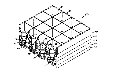
Fig. 1 i6 an isometric view, sectioned along a
6 Llhh~vt:Lr.e plane, of an antenna element according
7 to the present invention;
8 Fig. 2 shows part of Fig. 1 in greater detail, to
9 an enlarged scale;
Fig. 3 illustrates a preferred means used in
11 securing together parts of the assembly of Figs. 1
12 and 2;
13 Fig. 4 is a plan view illustrating the
14 co.~sLLu~;Lion of a modified form of waveguide
channel; and
16 Fig. 5 is an enlarged cross-sectional scrap view
17 on the line S-S of Fig. 4.
18
19 Referring particularly to Figs. 1 and 2, an antenna
element generally designated at 10 is in the form of a
21 4x4 array of receiving horns 12. In practice, the
22 element 10 would be assembled with like elements to
23 provide a larger array as a single antenna. The
24 antenna element 10 comprises five generally planar
members 14 - 22.
26
27 The first planar member 14 is formed to provide the
28 horns 12, each of which is of tAr~rin~ square section,
29 terminating in a lower wall 24 and circular tlpt~L Lul~:
26.
31
32 The second and third planar members 16, 18 together
33 define cylindrical cavities 28 aligned with the
34 circular apertures 26, and first closed, rectangular
section channels 30 extending along the length of the
,

21 ~80
Wo 9SI23440 P_ 1 .
antenna element 10. The cavities 28 terminate in a
2 plane partial end wall 32 defining a D-shaped slot 34.
4 The fourth and fifth planar members 20, 22 together
5 define bottom sections 36 to the horn cavities, and
6 second closed, rectangular section passages 38. Each
7 bottom section 36 has an upper part 39 ~,:VL r t,~vllding to
8 the D-shaped slots 34, and a lower part 40 forming an
9 open-topped channel ,_ n i cating with one of the
second passages 38.
11
12 The first ~hAnnP1R 30 c, icate with the cavities 26
13 by means of pas~as_yD 40 as indicated in Fig. 2.
14
15 Each of the planar members 14 - 22 is separately formed
16 by vacuum forming of a suitable plastics material.
17 T~rhniq~ of and materials for vacuum forming are well
18 known ~ and will not therefore be described in
19 detail herein. The walls of the horns, cavities and
20 ~hAnn~ have the effect of providing a corrugated
21 formation to each member, thus giving a reasonable
22 degree of rigidity which is increased when the five
23 members are secured together.
24
25 After vacuum forming, one side, as appropriate, of each
26 member is metallised in any suitable fashion, and thus
27 when the members are secured together the surfaces of
28 the horns, cavities and ~hAnn~ which are adjacent the
29 received microwave radiation are conductive metallised
30 surfaces . The ~ hAnn~ 30 and 38 thus act as
31 waveguides for differently polarised microwave signals
32 separated by the conformation of the cavities 26, as is
3 3 known ~ .
34
35 The f ive members may be secured together in any

2~ ~0~
wo gsl23440 r~
s
suitable manner. For example, they may be secured
2 together by adhesive. A preferred feature of the
3 present invention, however, i8 to 6ecure the planar
4 members together by mean6 of ultr;l~sn;r- welding. For
5 this purpose, as illustrated in Fig. 3, the mating
6 faces such as the lower face S0 of the first member 14
7 and the upper face 52 of the second member 16, are
B provided with ribs 54 which fuse to form cont
9 welded beads during ultrasonic welding.
11 Referring to Figs. 4 and 5, there is Lllustrated an
12 alternative cul".-Lu~;Lion of a moulded element 60 which
13 partially defines the wave guides, for example in
14 substitution for the element 22 in the above
: ~i . =
16
17 Fig. 4 shows a 12 x 12 array, but it will be understood
18 that the ~rrAn, L can be applied to any desired size
19 of array.
21 The element 60 is once again a vacuum forming in which
22 a single membrane of material is formed to provide
23 upper faces 62 and lower faces 64 joined by side webs
24 65 to define waveguide r~h~nn~l f; 66 . In this
25 embodiment, however, the upper faces 62 are defined
26 only as flanges in the vicinity of the waveguide
27 rhAnn~ 66, and elsewhere the material is cut away to
28 form void spaces 68.
29
30 This configuration is partic~ rly efficient and
31 results in a weight reduction of approximately 309~. In
32 addition, the particular design minimises the extent of
33 area which requires to be metallised.
3345

Representative Drawing
A single figure which represents the drawing illustrating the invention.
Administrative Status

2024-08-01:As part of the Next Generation Patents (NGP) transition, the Canadian Patents Database (CPD) now contains a more detailed Event History, which replicates the Event Log of our new back-office solution.

Please note that "Inactive:" events refers to events no longer in use in our new back-office solution.

For a clearer understanding of the status of the application/patent presented on this page, the site Disclaimer , as well as the definitions for Patent , Event History , Maintenance Fee  and Payment History  should be consulted.

Event History

Description Date
Inactive: IPC from MCD 2006-03-12
Application Not Reinstated by Deadline 2005-02-24
Time Limit for Reversal Expired 2005-02-24
Inactive: Abandoned - No reply to s.30(2) Rules requisition 2004-02-26
Deemed Abandoned - Failure to Respond to Maintenance Fee Notice 2004-02-24
Inactive: S.30(2) Rules - Examiner requisition 2003-08-26
Letter Sent 2002-04-19
Inactive: Application prosecuted on TS as of Log entry date 2002-04-19
Inactive: Status info is complete as of Log entry date 2002-04-19
Request for Examination Requirements Determined Compliant 2002-02-21
All Requirements for Examination Determined Compliant 2002-02-21
Inactive: Entity size changed 2002-02-12
Amendment Received - Voluntary Amendment 1996-11-20
Application Published (Open to Public Inspection) 1995-08-31

Abandonment History

Abandonment Date Reason Reinstatement Date
2004-02-24

Maintenance Fee

The last payment was received on 

Note : If the full payment has not been received on or before the date indicated, a further fee may be required which may be one of the following

  • the reinstatement fee;
  • the late payment fee; or
  • additional fee to reverse deemed expiry.

Please refer to the CIPO Patent Fees web page to see all current fee amounts.

Fee History

Fee Type Anniversary Year Due Date Paid Date
MF (application, 3rd anniv.) - small 03 1998-02-24 1998-02-09
MF (application, 4th anniv.) - small 04 1999-02-24 1999-02-02
MF (application, 5th anniv.) - small 05 2000-02-24 2000-02-21
MF (application, 6th anniv.) - small 06 2001-02-26 2001-01-31
MF (application, 7th anniv.) - standard 07 2002-02-25 2002-02-04
Request for examination - standard 2002-02-21
MF (application, 8th anniv.) - standard 08 2003-02-24 2003-02-06
MF (application, 2nd anniv.) - small 02 1997-02-24
Owners on Record

Note: Records showing the ownership history in alphabetical order.

Current Owners on Record
FORTEL TECHNOLOGY LIMITED
Past Owners on Record
JOHN LOUIS FREDERICK CHARLES COLLINS
Past Owners that do not appear in the "Owners on Record" listing will appear in other documentation within the application.
Documents

To view selected files, please enter reCAPTCHA code :


To view images, click a link in the Document Description column. To download the documents, select one or more checkboxes in the first column and then click the "Download Selected in PDF format (Zip Archive)" or the "Download Selected as Single PDF" button.

List of published and non-published patent-specific documents on the CPD .

If you have any difficulty accessing content, you can call the Client Service Centre at 1-866-997-1936 or send them an e-mail at CIPO Client Service Centre.


Document
Description 
Date
(yyyy-mm-dd) 
Number of pages   Size of Image (KB) 
Representative drawing 1997-10-14 1 17
Claims 1995-02-24 2 55
Drawings 1995-02-24 4 167
Description 1995-02-24 5 172
Abstract 1995-02-24 1 57
Cover Page 1995-02-24 1 15
Claims 1996-11-20 2 66
Reminder - Request for Examination 2001-10-25 1 118
Acknowledgement of Request for Examination 2002-04-19 1 180
Courtesy - Abandonment Letter (Maintenance Fee) 2004-04-20 1 175
Courtesy - Abandonment Letter (R30(2)) 2004-05-06 1 167
PCT 1996-08-23 9 354
Correspondence 1996-09-03 4 167
Fees 1997-01-28 1 49