Note: Descriptions are shown in the official language in which they were submitted.
2184147
DN 3030
COIN DETECTION DEVICE AND ASSOCIATED METHOD
Field of the Invention
This invention relates generally to vending machines and more particularly,
to coin detection devices and coin detection methods utilized in such vending
machines.
Background of the Invention
Known coin detection devices utilize various coin detection methods
including optical size detection and metallic characteristic detection. Two
such
coin detection devices are those disclosed in U.S. Patent No. 4,625,852 and
U.S. Patent No. 4,646,904. It is also known to combine optical size detection
and metallic characteristic detection in a single coin detection device in
order
to achieve greater coin detection accuracy. However, due to the similar
metallic content of some coins, it is difficult to distinguish between such
coins
using metallic characteristic detection. In such cases, even in coin detection
devices incorporating both types of coin detection, optical size detection
must
sometimes be relied upon to make the necessary distinction. Unfortunately, in
some cases, particularly in the case of ringed coins which are coins including
an
interior portion formed from a first material and a surrounding outer portion
-1-
2184147
DN 3030
formed from a second material, coins of various denominations may have
similar optical sizes making it difficult to distinguish between such coins.
Accordingly, it is desirable and advantageous to provide a coin detection
device capable of effectively distinguishing between coins having similar
metallic content. It also is desirable and advantageous to provide a coin
detection device which does not rely solely upon optical size detection to
distinguish between coins having similar metallic content.
Objects of the Invention
An object of the present invention is to provide a coin detection device and
associated method for distinguishing between coins of similar metallic
content.
Another object of the invention is to provide a coin detection device which
minimizes losses resulting from inaccurate validation of coins of similar
metallic content.
Another object of the present invention is to provide a coin detection
device which utilizes magnetic size detection in combination with optical size
detection to effectively distinguish between different coin types.
Yet another object of the present invention is to provide a method of coin
detection which can be implemented using known coin validation and/or
detection devices.
-2-
CA 02184147 2000-09-25
Summary of the Invention
These and other objects of the invention are attained by
a coin detection device which, in one embodiment, includes
first and second spaced optical sensors positioned along a coin
path and capable of detecting movements of a coin thereby. The
optical sensors may be configured such that a signal from each
optical sensor changes from a high (HI) state when there is no
coin detected by the optical sensor to a low (LO) state when
a coin is detected by the optical sensor. Such a construction
is disclosed in U.S. Patent No. 4,646,904 which is assigned to
the assignee of the present invention. The optical sensors
could also be configured to move from a LO state during non-
detection to a HI state during detection. A processing means,
such as a microprocessor, is connected to the optical sensors
so as to receive signals therefrom. The processing means is
also operable to establish an optical size time which runs from
when the coin is detected by the first optical sensor to when
the coin is detected by the second optical sensor. Further,
the optical size time preferably runs from when the coin is
first detected by the first optical sensor to when the coin is
last detected by the second optical sensor. However, it is
also understood that the present invention could be implemented
with only one optical sensor.
- 3 -
CA 02184147 2000-09-25
The coin detection device also includes a coil which is
energizable to produce an electromagnetic field in the region
of the coin path. In the embodiment described herein the coil
is part of a ringing circuit which is a modified version of the
ringing circuit described in U.S. Patent No. 4,625,852 which
is assigned to the assignee of the present invention. However,
the coil could be a part of numerous known coin detection
apparatus or circuits such as those which utilize a coil or
inductor as part of an oscillator circuit as disclosed in U.S.
Pat. Nos. 3, 870, 137; 3, 918, 563; 3, 918, 564; 3, 918, 565;
3, 952, 851; 3, 966, 034; and 4, 151, 904. The presence of the coin
in the region of, or field of, the coil of a ringing circuit
or oscillator circuit causes the output of such circuits to
change. Thus, the output of such circuits can be monitored
through various detector means or detector circuits, such as
described in the aforementioned patents, to determine the
presence or absence of the coin in the region of the coil. In
the coin detection device of the present invention, the
processing means is connected to the detector means and is
operable to establish a magnetic size time which runs from when
the coin enters the region of the coil and begins to affect the
field thereof, to when the coin leaves the region of the coil
and no longer affects the field thereof.
- 4 -
2184147
DN 3030
Having established the optical size time and the magnetic size time, the
processing means is also operable to establish either a magnetic to optical
size
ratio which is the ratio of the magnetic size time to the optical size time,
or the
reciprocal thereof. The established magnetic to optical size ratio is then
evaluated in light of stored predetermined maximum and minimum ratios for
the acceptable coin type or types to determine if the established magnetic to
optical size ratio falls within the maximum and minimum ratios for one of the
coin types. If the established magnetic to optical size ratio falls within
predetermined maximum and minimum values for a valid coin, then the tested
coin passes the magnetic to optical size ratio test.
Thus, the coin detection device of the present invention provides a
magnetic to optical size ratio test which is effective in distinguishing a
smaller
size, lower denomination coin from a larger size, higher denomination coin
even when the smaller coin has been modified to have the same optical size as
the larger coin. This magnetic to optical size ratio test can be utilized
alone or
in conjunction with other know tests for detecting and validating coins.
Brief Description of the Drawings
Fig. 1 is a side view of a coin in various positions while traveling along a
coin path;
-5-
2184147
DN 3030
Fig. 2 is a timeline diagram including times corresponding to each of the
coin positions illustrated in Fig. 1;
Fig. 3 is a block diagram illustration of the coin detection device of the
present invention;
Fig. 4 is a schematic circuit diagram of an embodiment of the coin
detection device illustrated in Fig. 2;
Fig. 5 is a side view of two coins formed of similar metals;
Fig. 6 is a flow chart illustration of a sequence of processing steps for the
subject coin detection device;
Fig. 7 is an illustration of a driving coil and a sensing coil in coupling
relation to each other; and
Fig. 8 is a side view of a coin in various positions while traveling along a
coin path.
Detailed Description of the Drawings
As shown in Fig. 1 a first optical sensor 10, a second optical sensor 12, and
a coil 14 are positioned along a coin path 16. The coil 14 is positioned
intermediate the optical sensors 10 and 12, however, the coil 14 could also be
positioned either to the left of optical sensor 10 or to the right of optical
sensor
12. Six positions of a coin 18 traveling from left to right along the coin
path
-6-
2184147
DN 3030
16 are depicted as dashed line circles designated one ( 1 ), two (2), three (3
),
four (4), five (5), and six (6). Position one (1) represents the position of
the
coin 18 when the coin 18 is first detected by the first optical sensor 10 and
position two (2) represents the position of the coin 18 when the coin 18 is
last
detected by the first optical sensor 10. Associated with the positions are
times
t, and tz which represent the points in time when the coin 18 will be located
at
positions one (1) and two (2) respectively. Similarly, at position five (5)
and
time t5 the coin 18 is first detected by the second optical sensor 12 and at
position six (6) and time t6 the coin 18 is last detected by the second
optical
sensor 12. With respect to the coil 14, at position three (3) and time t3 the
coin
18 is entering the region of the coil 14 and at position four (4) and time t4
the
coin 18 is leaving the region of the coil 14. Position three (3) is
representative
of when the coin 18 begins to interact with, or reaches a predetermined level
of
interaction with, the field of the coil 14, and position four (4) is
representative
of when the coin 18 is no longer interacting at the predetermined level, as
may
be indicated by various known methods, such as by a change in an output
signal of a detection circuit (not shown).
The present invention utilizes a magnetic to optical size ratio to distinguish
between different coins and between valid coins and slugs. However, it is
understood that the reciprocal of the magnetic to optical size ratio could be
2184147
DN 3030
used without departing from the scope of the present invention, in which case
the ratio would be appropriately termed an optical to magnetic size ratio.
The magnetic to optical size ratio is a ratio of the magnetic size time to the
optical size time. The magnetic size time is the time the coin 18 takes to
move
from position three (3) to position four (4), or (t4 - t3) as shown in the
timeline
of Fig. 2. The optical size time is the time the coin 18 takes to move between
the two optical sensors 10 and 12, preferably between positions one (1) and
six
(6), or (t6 - t,). Further, although not required, it may be desirable to
multiply
the ratio by a constant K. Thus, the magnetic to optical size ratio
(RATIOz"ro)
may be represented by the equation RATIOM,o = [(t4 - t3 )/(t6 - t,)]K. In this
ratio, time t3 is dependent upon the position of the leading edge of the coin
18
while time t4 is dependent upon the position of the trailing edge of the coin
18.
Therefore, the travel time (t6 - t,) between positions one (1) and six (6) is
preferred for purposes of the optical size time or denominator because time t,
is similarly dependent upon the position of the leading edge of the coin 18
and
time t6 is similarly dependent upon the position of the trailing edge of the
coin
18. Due to this symmetry between the two time periods, (t4 -t3) and (t6 - t,),
a
ratio of the two is substantially independent of the speed of the coin. Thus,
although other travel times such as (ts - t2), (t5 - t,), or (t6 - tz) could
be used in
the denominator, the magnetic to optical size ratio is most effective for
_g_
21 X4147
DN 3030
distinguishing between coins when the travel time (t6 - t,) is used as the
optical
size time in the denominator.
The particular travel times utilized in the magnetic to optical size ratio can
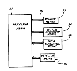
be established by the coin detection device 20 illustrated in block diagram
form
in Fig. 3. The coin detection device 20 includes a processing means 22, such
as a microprocessor, connected to an optical detection means 24 which
includes the optical sensors 10 and 12 illustrated in Fig. 1. Also connected
to
the processing means 22 is a field generating means 26 which includes the coil
18 of Fig. l and may comprise various known field generating means commonly
used in coin detection devices. A detector means 28 is associated with the
processing means 22 and the field generating means 26 such that the detector
means 28 is able to detect when the coin 18 enters and leaves the region of
the
coil 14 and its associated field. Again, the detector means 28 utilized may
include detector means such those used in known coin detection devices.
The processing means 22 is also connected to a memory means 30 such
that the processing means 22 is capable of retrieving stored information
therefrom. In operation, the coin detection device 20 establishes the magnetic
to optical size ratio described above with reference to Figs. 1 and 2, and the
established magnetic to optical size ratio is evaluated in light of
predetermined
maximum and minimum ratios for acceptable coins, which maximum and
-9-
2184141
DN 3030
minimum ratios are stored in the memory means 30. In this regard, the coin
detection device 20 may be configured to compare the established magnetic to
optical size ratio with one set of a predetermined maximum ratio and a
predetermined minimum ratio for a single coin type or the coin detection
device 20 may be configured to compare the established ratio with a plurality
of sets of predetermined maximum and predetermined minimum ratios for a
corresponding plurality of coin types. In either case, if the established
magnetic to optical size ratio falls between the predetermined maximum and
minimum ratios for a particular valid coin type, then the coin being tested is
accepted as satisfying the magnetic to optical size ratio test for that
particular
coin type.
Fig. 4 illustrates a schematic circuit diagram of the optical detection means
24, the field generating means 26, and the detection means 28 illustrated in
Fig.
3. This particular embodiment is intended for illustration purposes only and
it
is understood that the implementation of the magnetic to optical size ratio
test
is not necessarily limited to the Fig. 4 embodiment. The circuitry to the
right
of line 31 is indicated as prior art. Further, while the processing means 22
and
the memory means 30 are not considered structurally new, the programming of
the processing means 22 and the information stored in the memory means 30
and used by the processing means 22 result in a novel coin detection device.
-10-
218447
DN 3030
The optical detection means 24 includes the optical sensors 10 and 12, each
forming an optical coupler pair including a light emitting diode 32 or 34 and
corresponding phototransistor 36 or 38. Each light emitting diode 32 and 34 is
positioned on one side of the coin path 16, shown in Fig. 1, and each
corresponding phototransistor 36 and 38 is positioned on the opposite side of
the coin path 16. The optical coupling of each pair places the phototransistor
36 or 38 in a conductive state so that a HI signal is transmitted to the
processing means along lines 40 or 42. When a coin passes between an optical
coupler pair the optical coupling between the pair is broken and the
phototransistor 36 or 38 switches to a non-conductive state such that a LO
signal is transmitted to the processing means 22. Thus, each optical sensor 10
and 12, or optical coupler pair, is capable of detecting when a coin passes
therebetween. The processing means 22 is programmed to utilize the signals
from the optical sensors 10 and 12 to establish the optical size time
described
above.
The field generating means 26 includes the coil 14 connected in parallel
with a capacitor 44 to form a tank circuit 46. The input of the tank circuit
46
is connected to a power supply means 47. The circuit illustrated in Fig. 4 is
a
modified version of the circuit illustrated and described in Fig. 3 of U. S.
Patent
No. 4,625,852. As is evident from the description contained therein, the tank
-11-
2184147
DN 3030
circuit 46 is connected to both an output monitor lead 48 and through a
resistor 50 to a driver means 52 whose input is connected to a control link
54.
When a LO ring initiation signal is applied to the control line 54, the output
of
the driver means 52 will go HI causing the tank circuit 46 to be interrupted
in
such manner that a damped wave output signal is produced on monitor lead
48.
The output monitor lead 48 is connected to the positive input (+) of a
voltage comparator 56, the negative input (-) of which is connected to a
reference lead 58 which in turn is connected to the output of a digital to
analog
converter 60 such that a controllable reference voltage is applied to the
negative input (-). The output 62 of the voltage comparator 56 is connected
to a positive voltage source through a pull-up circuit 64 so that whenever the
voltage at the negative input (-) is less than the voltage of the positive
input
(+), a HI signal is ensured at the output 62. When the tank circuit 46 is rung
so as to provide a damped wave output signal as described above, the damped
wave signal is compared against the reference voltage and the output 62 is fed
into a counter 66. Each time the damped signal voltage drops below the
reference voltage a count is triggered in the counter 66. For purposes of the
present invention the reference voltage can be chosen such that when the
counter 66 counts a predetermined number (m) for a ringing operation, the
-12-
2184147
DN 3030
count number (m) is indicative of the coin 18 having entered the region of the
coil 14 or of the coin 18 having reached a predetermined level of interaction
with the field of the coil 14. Similarly, when the coin 18 leaves the region
of
the coil 14 the count for a ringing operation will no longer reach the
predetermined count number (m). Thus, the coin detection device 20 is able to
detect when the coin 18 enters the region of the coil 14 and when the coin 18
leaves the region of the coil 14. The reference voltage and/or count number
(m) may be varied as desired to detect different levels of interaction between
the coin 18 and the coil 14.
With respect to the ringing of tank circuit 46, it is understood that the
detection of a coin by optical sensor 10, shown in Fig. 1, could be utilized
to
initiate a series of ringing operations. However, the tank circuit 46 could
also
be continuously rung regardless of whether or not a coin is traveling along
the
coin path 16.
Based upon signals from the counter 66, the processing means 22 is
operable to establish the magnetic size time described above. Once both the
magnetic size time and the optical size time have been established, the
processing means 22 then establishes the magnetic to optical size ratio and
evaluates the ratio in light of the predetermined maximum and minimum ratios
stored in the memory means 30.
-13-
2184147
DN 3030
The advantage of the present invention can be seen with reference to Fig. S
which illustrates a first ringed coin 68 and a second ringed coin 70. The
first
coin 68 includes an inner portion A formed of Copper (Cu) and an outer
portion B formed of Nickel (Ni). The second coin 70 includes an inner portion
A' formed of Ni and an outer portion B' formed of Cu. Thus, the coins have
similar metallic content, although the location of the particular metals is
reversed. As illustrated, the optical size of the first coin 68 is the same as
the
optical size of the second coin 70, both D 1. With respect to magnetic size,
however, because Ni will have a greater effect than Cu on the coil 14 and its
associated circuit, the magnetic size time for the first coin 68 will be
longer
than the magnetic size time for the second coin 70. Accordingly, the magnetic
to optical size ratio of the first coin 68 will be different than the magnetic
to
optical size ratio of the second coin 70 and the coin detection device 20 will
be
able to distinguish between the first coin 68 and the second coin 70.
Fig. 6 illustrates a sequence of processing steps which could be
programmed into processing means 22. The particular processing steps shown
would be utilized with the sensor configuration shown in Fig. 1, where the
coil
14 is located intermediate the optical sensors 10 and 12. Also, the processing
steps illustrated in Fig. 6 implement an optical size time based on positions
six
(6) and one (1) of the coin 18. It is understood that other processing steps
-14-
2184147
DN 3030
could be utilized and that numerous routines could be incorporated into each
processing step depending upon the particular sensor configuration of the coin
detection device and also depending upon the optical size time which is being
implemented.
The sequence starts at 100 and moves to step 102. When the coin reaches
position one (1), see Fig. 1, the optical coupling of the first optical sensor
is
blocked and the signal sent to the processing means 22 along line 40, see Fig.
4, goes LO and processing moves to step 104 where time t, is set. When the
coin 18 begins to interact with the field of the coil at position three (3),
decision step 106 is satisfied and time t3 is set at step 108. When the coin
no
longer interacts with the field of the coil at position four (4), decision
step 110
is no longer satisfied and time t4 is set at step 112. When the coin reaches
position five (5), decision step 114 is satisfied and processing moves to step
116. When the coin reaches position six (6), decision step 116 is satisfied
and
time t6 is set at step 118. At step 120 the magnetic size time (MAGT) is
determined and at step 122 the optical size time (OPTT) is determined. The
magnetic to optical size ratio is then determined at step 124 and at step 126
the magnetic to optical size ratio is evaluated to see if it satisfies
predetermined
criteria of a valid coin type. Processing then ends at step 128.
-15-
2184141
DN 3030
As previously explained, the optical detection means 24, field generating
means 26 and detector means 28 could include numerous known constructions
common to existing coin detection devices. For example, the field generating
means could include a driving coil 72 as illustrated in Fig. 7 while the
detector
means could include an associated sensing coil 74 in which a voltage VI is
induced by the generated field. In this configuration, which is well known in
the art, the level of interaction of the coin with the field of the driving
coil 72
would be indicated by changes in the voltage VI induced in the sensing coil 74
Further, the optical detection means could be a single optical sensor 76 such
as
that illustrated within the coil 78 of Fig. 8, the coil 78 being wound on a
core
within which the optical sensor 76 is located. In this embodiment, the
magnetic to optical size ratio would be based upon coin positions A1, A2, A3,
and A4 as represented by the equation
RATIOI,,fo - [(tn4 - tA,)/(t~-t"~)]K. Moreover, the optical sensor 76 could
also
be located to one side of the coil 78.
From the preceding description, it is evident that the objects of the
invention are attained. In particular, a coin detection device which is
capable
of distinguishing between coins of similar metallic content without relying
solely on optical size testing has been provided. Further, a method of coin
detection which can be implemented utilizing various known coin validation
-16-
2184147
DN 3030
and/or detection devices has also been provided. Although the invention has
been described and illustrated in detail, it is to be clearly understood that
the
same is intended by way of illustration and example only and is not to be
taken
by way of limitation. For example, the coin detection method of the present
invention could be implemented in many existing coin validation and/or
detection devices. Accordingly, the spirit and scope of the invention are to
be
limited only by the terms of the appended claims.
-17-