Note: Descriptions are shown in the official language in which they were submitted.
i.218422
WIDE RANGE VARIABLE OUTPUT
AMPLIFIER APPARATUS WITH HIGH EFFICIENCY
BACKGROUND OF THE INVENTION
Field of the Invention
The present invention relates to a variable output
amplifier apparatus used in a transmitter for mobile communica-
tions or the like which imposes severe restrictions on power
dissipation.
Description of the Related Art
Generally, a communication state of mobile communica-
tion apparatuses is poor as compared with a communication state
of wire communication apparatuses. Particularly, in the mobile
communication apparatuses, the level of reception signals
fluctuates greatly. For example, in cellular telephones, the
range of this intensity is about 80 dB to 100 dB.
In a prior art mobile communication system, since it
is difficult to superimpose information on the amplitude
components of carriers, such information is superimposed on the
frequency components of the carriers, which is called constant
envelope modulation. According to this modulation, it is
possible to reproduce original information by carrying out a
nonlinear processing such as saturation amplification, and also,
it is possible to remove harmonic components due to the
saturation amplification by using bandpass filters. Therefore,
saturation amplification is carried out both in transmission
and reception. As a result, in a receiving apparatus, the
above-mentioned large fluctuation of received signal level is
- 1 -
75702-5
absorbed. On the other hand, in a transmitting apparatus,
effective use is made of a power supply by employing the
efficiency of the nonlinear amplification.
Incidentally, as demands for mobile communications
have been increasing, linear modulation systems and multi-
valued transmission systems have been considered. In the
linear modulation systems and the multi-valued transmission
systems, however, if a nonlinear processing is carried out,
the occupied bandwidth is broadened, and the information
superimposed on the amplitude of carriers is destroyed. Thus,
a wide range variable output amplifier apparatus is required
in a transmitter side and a receiving side of such systems.
On the other hand, in a direct sequence code division
multiple access (DS-CDMA) system in which a plurality of mobile
stations use the same frequency band simultaneously, a base
station has to receive signals from all the mobile stations at
approximately the same level. That is, if the intensity of a
signal from one mobile station is too strong, it is difficult
to exclude its effect on the other mobile stations, which
reduces actual transmission capacity. Thus, a wide range
variable output amplifier apparatus is also required in the
transmitting side of the systems.
In a first prior art variable output amplifier
apparatus for a power transmission system (see: JP-A-58-83437),
an input signal is amplified by first and second power
amplifiers. A part of an output signal of the second power
amplifier is fed back by a directional coupler to a detector.
- 2 -
75702-5
--Z184225
The directional coupler also feeds an output signal. A control
circuit compares an output of the detector with a reference
voltage, and as a result, a power supply of the first power
amplifier is controlled in accordance with the comparison result
of the output of the detector with the reference voltage. In
addition, when the transmission power is low, a changeover
switch is selected, so that the power supply of the second power
amplifier is switched to the same power supply for the first
power amplitude. This will be explained later in detail.
In the first prior art apparatus, however, when the
changeover switch is switched, a large noise spike is generated
during a transient state. Also, since the gains of the power
amplifiers are controlled by their power supply, the input/output
impedance conditions of the power amplifiers are changed.
Further, the operation of the detector over a wide range (from
approximately 80 dB to l00 dB) is too difficult.
In a second prior art variable output amplifier
apparatus (see: JP-A-60-2120l3), a plurality of first amplifiers
are connected in parallel for receiving an input signal. The
first amplifiers are connected via a first changeover switch to
a plurality of second amplifiers connected in parallel which are
connected via a second changeover switch to a detector. The
second changeover switch feeds an output signal. The output
signal of the detector is supplied to a selection determination
circuit for controlling the changeover switches. In particular,
the selection determination circuit selects an optimum combina-
tion of one of the first amplifiers and one of the second
- 3 -
75702-5
amplifiers in accordance with the output of the detector. This
will also be explained later in detail.
Even in the second prior art apparatus, however, when
the changeover switches are switched to control the gain, a
large noise spike is generated during a transient state. Also,
changing the signal path causes a change in the delay time, and
thus, an interruption may occur in an otherwise continuous
signal.
SUMMARY OF THE INVENTION
It is an object of the present invention to provide
a wide range variable output apparatus with a high efficiency.
According to the present invention, in a variable
output amplifier apparatus, an input signal is distributed by
a distributing unit as first signals to a plurality of variable
gain units having different gain and maximum output power.
Second signals generated from the variable gain units are
combined by a combining unit to generate an output signal. A
plurality of power supply control units apply power to each of
the variable gain units, respectively. The variable gain units
and the power supply control units are controlled by a control
unit. When one of the variable gain units and one of the power
supply control units are activated, the corresponding power
supply is rapidly turned ON. When they are deactivated, the
corresponding power supply is slowly turned OFF.
When the power supply is rapidly turned ON, the gain
of the corresponding variable gain unit is still low, so that
noise due to the turning ON of the power supply can be
- 4 -
75702-5
~~8~225
neglected. Also, when the power supply is slowly turned OFF,
the gain of the corresponding variable gain unit is already
low, so that noise due to the turning OFF of the power supply
can be also neglected.
In accordance with the present invention, there is
provided a variable output amplifier apparatus, comprising: a
distributing unit for receiving an input signal to generate a
plurality of first signals; a plurality of variable gain units
connected to said distributing unit, each of said variable gain
units having a gain for amplifying said first signals and out-
putting second signals; a combining unit, connected to said
variable gain units, for combining said second signals into an
output signal; a plurality of power supply control units, each
connected to one of said variable gain units, for applying
power supplies to said variable gain units; and a control unit,
connected to said variable gain units and said power supply
control units, for controlling said variable gain units and
said power supply control units, a first one of said variable
gain units and a first one of said power supply control units
connected to said first variable gain unit being activated by
said control unit, so that said first power supply control unit
promptly turns ON the power supply applied to said first
variable gain unit before the gain of said first variable gain
unit is gradually increased from a first minimum vlue to a
first maximum value, a second one of said variable gain units
and a second one of said power supply control units connected
to said second variable gain unit being deactivated by said
_ 5 _
".,
75702-5
control unit, so that said second power supply control unit
turns OFF the power supply applied to said second variable gain
unit after a time period has passed and the gain of said second
variable gain unit is gradually decreased from a second maximum
value to a second minimum value.
In accordance with another aspect of the invention,
there is provided a variable output amplifier apparatus,
comprising: a distributing unit for receiving an: input signal
to generate a plurality of first signals; a plurality of
variable gain units connected to said distributing unit, for
amplifying said first signals and outputting second signals,
wherein each of said variable gain units comprises: a first
variable attenuation unit for receiving one of said first
signals, said first variable attenuation unit being controlled
by said control unit; a fixed gain unit connected to said first
variable attenuation unit, said fixed gain unit being powered
by one of said power supplies; a second variable attenuation
unit connected to said fixed gain unit; and a delay unit,
connected to said second variable attenuation unit, for
generating one of said second signals, said delay unit being
powered by one of said power supplies; and wherein maximum
attenuations of said first and second variable attenuation
units being larger than a maximum gain of said fixed gain unit;
said variable output amplifier apparatus further comprising:
a combining unit, connected to said variable gain units, for
combining said second signals into an output signal; a plurality
of power supply control units, each connected to one of said
- 6 -
.,.- ;.,,...
,_,t .
~.,a.
75702-5
2184225
variable gain units, for applying power supplies to said
variable gain units; and a control unit, connected to said
variable gain units and said power supply control units for
controlling said variable gain units and said power supply
control units, a first one of said variable gain units and a
first one of said power supply control units connected to said
first variable gain unit being activated by said control unit,
so that said first power supply control unit turns ON the power
supply applied to said first variable gain unit, a second one
of said variable gain units and a second one of said power
supply control units connected to said second variable gain
unit being deactivated by said control unit, so that said second
power supply control unit turns OFF the power supply applied to
said second variable gain unit.
BRIEF DESCRIPTION OF THE DRAWINGS
The present invention will be more clearly understood
from the description as set forth below, in comparison with the
prior art, with reference to the accompanying drawings, wherein:
Fig. 1 is a block diagram illustrating a first prior
art variable output amplifier apparatus;
Fig. 2 is a block diagram illustrating a second prior
art variable output amplifier apparatus;
Fig. 3 is a block diagram illustrating a first
embodiment of the variable output amplifier according to the
present invention;
Fig. 4 is a diagram showing gains of the variable gain
units of Fig. 3;
,.. ~-.~~t
,.
7 _
75702-5
Figs. 5A through 5E are timing diagrams showing the
operation of the apparatus of Fig. 3;
Fig. 6 is a block diagram illustrating a second
embodiment of the variable output amplifier according to the
present invention;
Figs. 7A, 7B, 7C and 7D are timing diagrams showing
operation of the control unit of Fig. 6;
Fig. 8 is a detailed block diagram of each of the
variable gain units of Figs. 3 and 6;
Fig. 9 is a block diagram illustrating a modification
of the variable gain unit of Fig. 8; and
Fig. 10 is a detailed circuit diagram of the power
supply control circuit of Figs. 3 and 6.
DESCRIPTION OF THE PREFERRED EMBODIMENTS
Before the description of the preferred embodiments,
prior art variable output amplifier apparatuses will be
explained with reference to Figs. 1 and 2.
Fig. 1 illustrates a first prior art variable output
amplifier apparatus for a power transmission system (see:
JP-A-58-83437). An input signal SIN is amplified by power
amplifiers 101 and 102. A part of an output signal of the
power amplifier 102 is fed back by a directional coupler 103
to a detector 104. The directional coupler 103 also feeds an
output signal SOUT' A control circuit 105 compares a trans-
mission power level detected by the detector l04 with a
reference voltage VREF' and as a result, a power supply VCC
of the power amplifier l01 is controlled in accordance with the
_ g _
,~si
75702-5
2184225
comparison result of the transmission power level with the
reference voltage VREF' In addition, when the transmission
power is low, a changeover switch l06 is selected at an upper
position, so that the power supply of the power amplifier l02
is switched from VCC to VCC~'
In Fig. 1, however, when the changeover switch 106 is
switched, a large noise spike is generated during a transient
state. Also, since the gains of the power amplifiers 101 and
l02 are controlled by their power supply, the input/output
impedance conditions of the power amplifiers 101 and 102 are
changed. Generally, when the power supply is greatly changed,
it is very difficult to maintain the characteristics of the
power amplifier. Further, the operating of the detector 104
over a wide range (from approximately 80 dB to l00 dB) is too
difficult.
Fig. 2 illustrates a second prior art variable output
amplifier apparatus (see: JP-A-60-2120l3). Four amplifiers
201 through 204 are connected in parallel for receiving an
input signal SIN. The amplifiers 20l through 204 are connected
via a changeover switch 205 to four amplifiers 206 through 209
which are also connected in parallel. The four amplifiers 206-
209 are connected via a changeover switch 210 to a detector 211.
The changeover switch 210 feeds an output signal SHUT' The
output signal of the detector 2l1 is supplied to a selection
determination circuit 212 for controlling the changeover
switches 205 and 210. In particular, the selection determinatica~
circuit 212 selects an optimum combination of one of the
- 9 -
75702-5
'~
~. ~
amplifiers 201 through 204 and one of the amplifiers 206 through
209 in accordance with the output of the detector 211.
In Fig. 2, however, when the changeover switches 205
and 2l0 are switched to control the gain, a large noise spike
is generated during a transient state. Also, changing the signal
path changes the delay time, and thus an interruption may occur
in an otherwise continuous signal.
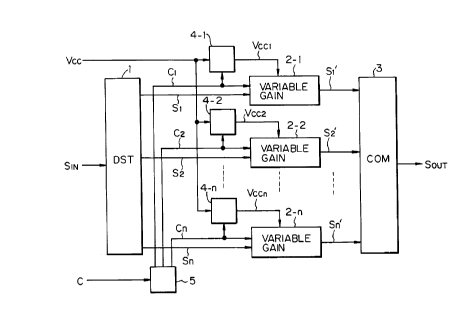
Fig. 3 illustrates a first embodiment of the present
invention. A distributing unit 1 distributes an input signal
SIN as signals S1, S2, . ., Sn to variable gain units 2-1, 2-2,
..., 2-n, respectively. Output signals S1', S2', . ., Sn' of
the variable gain units 2-1, 2-2, ..., 2-n are combined by a
combining unit 3 to generate an output signal SOUT'
Power supply voltages VCCl' VCC2' " '' VCCn are
applied to the variable gain units 2-1, 2-2, . ., 2-n from power
supply control units 4-1, 4-2, . ., 4-n, respectively, which
commonly receive a power supply VCC.
The variable gain units 2-1, 2-2, . ., 2-n and the
power supply control units 4-l, 4-2, . ., 4-n are controlled by
control signals Cl, C2, ..., Cn, respectively, of a control unit
5 which receives a gain control signal C. When the control
signal C1 is sloped from low to high, for example, the power
supply control unit 4-1 promptly raises the power supply VCCl
from GND to VCC, and then the gain of the variable gain unit 2-1
gradually starts to change from the minimum value to the maximum
value. On the other hand, when the control signal Cl is sloped
from high to low, the gain of the variable gain unit 2-1 starts
- 10 -
",... .;...
ync._
75702-5
_ 2184225
to gradually change from the maximum value to the minimum
value, and then the power supply control unit 4-1 switches the
power supply VCC1 from VCC to GND.
Examples of the gains of the variable gain units 2-1,
2-2, ..., 2-n are shown in Fig. 4. In particular, the gain of
the variable gain unit 2-1 ranges from MAX1 to MIN1; the gain
of the variable gain unit 2-2 ranges from MAX2 to MIN2; ...;
and the gain of the variable gain unit 2-n ranges from MAXn to
MINn. In this case, the value MINI is smaller than the value
MAX2, the value MIN2 is smaller than value MAX3, and so on.
An example of the operation of the variable amplifier
apparatus of Fig. 3 is explained next with reference to Figs. 5A
through 5E.
First, at time t0, the control signals C1 and C2 are
VCC and GND, respectively, as shown in Figs. 5A and 5B, and
accordingly, the power supplies VCC1 and VCC2 are VCC and GND,
respectively, as shown in Figs. 5C and 5D. Also, the gain of
the variable gain unit 2-1 is MAX1, and the gain of the variable
gain unit 2-2 is MIN2, as shown in Fig. 5E.
Next, at time tl, the control signal C1 starts to
slope from VCC to GND, and almost simultaneously, at time tl',
the control signal C2 starts to slope from GND to VCC. As a
result, the power supply VCC2 is switched by the power supply
control unit 4-2 from GND to VCC. Here, noise may be generated
due to the rising of the power supply VCC2 in the variable gain
unit 2-2, however, such noise can be neglected since the gain
of the variable gain unit 2-2 is still substantially equal to
MIN2. Also, as shown in Fig. 5E, the gain of the variable gain
- 11 -
75702-5
unit 2-1 is gradually decreased by the falling of the control
signal Cl, and the gain of the variable gain unit 2-2 is
gradually increased.
At time t2, the gain of the variable gain unit 2-1
reaches MLNl, while the gain of the variable gain unit 2-2
reaches MAX2.
Finally, at time t3, the power supply VCC1 is switched
by the power supply control unit 4-1 from VCC to GND. Here,
noise may be generated due to the falling of the power supply
VCC1 In the variable gain unit 2-1, however, such noise can be
neglected since the gain of the variable gain unit 2-1 is
already MIN1.
Note that a signal delay of each of the variable gain
units 2-1, 2-2, ..., 2-n is equalized through the maximum gain
control state to the minimum gain control state. Therefore,
the output signal S~UT ~f the combining unit 3 is smoothly
switched from the maximum gain of the variable gain unit 2-1
to the maximum gain of the variable gain unit 2-2.
Generally, the larger the gain of the variable gain
unit, the larger the power dissipation. Therefore, one of the
variable gain units 2-l, 2-2, ..., 2-n which are optimized its
power dissipation at its maximum output power is selected, which
can use the power supply effectively.
Also, in the variable output amplifier apparatus of
Fig. 3, if only one of the variable gain units 2-1, 2-2, ...,
2-n is selected, the gain of the apparatus of Fig. 4 can be
discretely changed from MAX1, MAX2, ..., MAXn,to MIN1, MIN2,
- 12 -
-<;~~-:
_.,' . ,,s.
75702-5
w 2184225
..., MINn as shown in Fig. 3. Therefore, if the number of the
variable gain units 2-1, 2-2, ..., 2-n is increased, the gain
of the apparatus of Fig. 3 can be almost continuously changed
from MIN1 to MAXn.
In Fig. 6, which illustrates a second embodiment of
the present invention, a variable gain unit 6 is added to the
elements of Fig. 3, thus obtaining a completely continuous
change of the gain of the apparatus. The variable gain unit 6
is controlled by a control signal CO that is generated by a
control unit 5'. In this case, the range of gain of the
variable gain unit 6 is small, for example, from 0 to MAX,
where MAX is larger than MAX2 in Fig. 4.
An example of the operation of the control unit 5'
is explained with reference to Figs. 7A, 7B, 7C and 7D. Here,
assume that the gain control signal C is gradually decreased so
that the variable gain units 2-1, 2-2, ..., 2-n are sequentially
activated as shown in Figs. 7A, 7B and 7C. In this case, as
shown in Fig. 7D, the level of the gain control signal CO for
the variable gain unit 6 is gradually and stepwise decreased
as the gain control signal C is gradually decreased. Therefore,
the control unit 5' can be formed by a voltage divider or the
like in addition to the elements of the control unit 5 of
Fig. 3 .
Each element of the apparatuses of Figs. 3 and 6 will
be explained next.
Ln Fig. 8, which is a detailed circuit diagram of the
variable gain unit 2-i (i = 1, 2, ..., n) of Figs. 3 and 6, the
- 13 -
75702-5
signal Si pas.ses through a variable attenuation unit 801, a
fixed gain unit 802, a variable attenuation unit 803 and a
delay unit 804. In this case, the variable attenuation units
801 and 803 are controlled by the control signal Ci, while the
fixed gain unit 802 and the delay unit 804 are activated by
the power supply UCCi' The maximum attenuations of the variable
attenuation units 801 and 803 are larger than the maximum gain
of the fixed gain unit 802. The delay time of the delay unit
804 compensates the fluctuation of the variable attenuation
units 801 and 803 so that the delay times of the variable gain
units 2-1, 2-2, ..., 2-n are equalized.
Also, the attenuations of the variable attenuation
units 801 and 803 defining the gain of the variable gain unit
2-i are gradually changed in response to the change of the
control signal Ci. Thus, the gain of the variable gain unit
2-i is gradually changed as shown in Fig. 5E.
Further, the fixed gain unit 802 is turned ON and OFF
when the attenuations of the variable attenuation units 801 and
803 are maximum. Therefore, even when the input/output
impedance of the fixed gain unit 802 is fluctuated, there is no
adverse effect on the input signal Si and the output signal Si'.
In Fig. 9, which is a modification of the variable
gain unit 2-i of Fig. 8, a delay unit 901 is provided instead
of the delay unit 804 of Fig. 8. In particular, the delay unit
90l is also controlled by the control signal Ci, so that the
delay time of the entire variable gain unit 2-i is almost
constant regardless of the change of the gain thereof'
- 14 -
r..._
75702-5
.~ 21g4225
In Fig. 10, which is a detailed circuit diagram of
the power supply control unit 4-i (i = l, 2, ..., n) of Figs. 3
and 6, a comparator CMP compares the voltage of the signal Ci
with a reference voltage VR defined by resistors R1 and R2, so
as to control an N-channel MOS transistor Qn. Also, a
P-channel MOS transistor Qp is interposed between an input for
the power supply VCC and an output for the power supply VCCi'
and is controlled by the N-channel MOS transistor Qn. Further,
a resistor R3 is connected between the gate of the P-channel
MOS transistor Qp and the input for the power supply VCC'
When the voltage of the signal Ci becomes higher than
VR, the comparator CMP turns ON the N-channel MOS transistor
Qn, so that the gate voltage of the P-channel MOS transistor
Qp becomes low (= GND). As a result, the P-channel MOS
transistor Qp is rapidly turned 01V. Thus, the power supply
VCCi rapidly becomes VCC (see Figs. 5B and 5D).
On the other hand, when the voltage of the signal Ci
becomes lower than VR, the comparator CMP turns OFF the
N-channel MOS transistor Qn. However, in this case, due to
the presence of the resistor R3, the gate voltage of the
P-channel MOS transistor Qp becomes high (= VCC). As a result,
the P-channel MOS transistor Qp is turned OFF. Thus, the power
supply VCCi becomes GND (see Figs' 5A and 5C)'
As explained hereinabove, according to the present
invention, a large amount of noise due to the switching of the
power supply can be avoided. Also, the power supply can be
used effectively.
- 15 -
,F:ry\ I~3~4
i~v:9
' 75702-5