Note: Descriptions are shown in the official language in which they were submitted.
CA 02184496 2001-03-21
64159-1481
1
LIGHThIAVE PHASE CONTROL FOR REDUCTION OF
RESONATOR FIBER OPTIC GYROSCOPE KERR EFFECT ERROR
Reference is hereby made to the U.S. Patent 5,349,441
assigned to Honeywell Inc. entitled "Fiber Optic Gyroscope
Refractive Index Induced Error Compensation".
BACKGROUND OF THE INVENTION
The present invention relates to fiber optic
gyroscopes used for rotation sensing and, more particularly, to
resonator fiber optic gyroscopes.
l0 Fiber optic gyroscopes are an attractive means with
which to sense rotation. They can be made quite small and
still be constructed to withstand considerable mechanical
shock, temperature change, and other environmental extremes.
In the absence of moving parts, they can be nearly maintenance
free, and they have the potential to become economical in cost.
They can also be sensitive to low rotation rates that can be a
problem in other kinds of optical gyroscopes.
There are various forms of optical inertial rotation
sensors which use the well known Sagnac effect to detect
rotation about a pertinent axis thereof. These include active
optical gyroscopes having the gain medium contained in an
optical cavity therein, such as the ring laser gyroscope, and
passive optical gyroscopes without any gain medium in the
primary optical path, such as the interferometric fiber optic
gyroscope and the ring resonator fiber optic gyroscope. The
avoidance of having the active medium along the primary optical
path in the gyroscope eliminates some problems which are
encountered in active gyroscopes such as low rotation rate
lock-in, bias drift and some causes of scale factor variation.
CA 02184496 2001-03-21
64159-1481
la
Interferometric fiber optic gyroscopes typically
employ a single spatial mode optical fiber of a substantial
length formed into a coil, this substantial length of optical
fiber being relatively costly. Resonator fiber optic
gyroscopes, on the other hand, are constructed with relatively
few turns of a single spatial mode optical fiber giving them
the potential of being more economical than interferometric
fiber optic gyroscopes. A resonator fiber optic gyroscope
typically has three to fifty meters of optical fiber in its
coil versus 100 to 2,000 meters of optical fiber in coils used
in interferometric fiber optic gyroscopes. In addition,
resonator fiber optic gyroscopes appears to have certain
advantages in scale factor linearity and dynamic range.
In either type of passive gyroscopes, these coils are
part of a substantially closed optical path in which an
electromagnetic wave, or light wave, is introduced and split
into a
218449b
WO 95!24611 PCTIUS95/02908
-2-
pair of such waves, to propagate in opposite directions through the optical
fiber coil to
both ultimately impinge on a photodetector or photodetectors, a single
photodetector for
both waves in interferometric fiber optic gyroscopes and on corresponding ones
of a pair
of photodetectors in resonator fiber optic gyroscopes. Rotation about the
sensing axis of
the core of the coiled optical fiber in either direction provides an effective
optical path
length increase in one rotational direction and an effective optical path
length decrease in
the opposite rotational direction for one member of this pair of
electromagnetic waves.
The opposite result occurs for the remaining member of the pair of
electromagnetic waves
for such rotation. Such path length differences between the pair of
electromagnetic waves
introduce corresponding phase shifts between those waves in interferometric
fiber optic
gyroscopes, or cor esponding different optical cavity effective optical path
lengths for
these waves in a resonator fiber optic gyroscope.
In this latter instance, one or more optical frequency shifters are used to
each
effectively adjust the frequency of a corresponding one of the pair of
electromagnetic
waves that circulate in opposite directions in the resonator fiber optic coil.
This is
accomplished through such a frequency shifter shifting the frequency of a
corresponding
input electromagnetic wave giving rise to the resonator electromagnetic wave
of interest.
As a result, through feedback arrangements. the frequencies of each member of
the pair of
electromagnetic waves can be kept in resonance with the effective optical path
length that
wave is experiencing in the resonator fiber optic coil. Hence, any frequency
difference
between these waves becomes a measure of the rotation rate experienced by the
resonator
fiber optic coil about the axis around which this coil has been positioned. In
such
resonances, each wave has the portions thereof that previously were introduced
in the
resonator coil and have not yet dissipated, and the portions thereof currently
being
introduced in the resonator coil, at a frequency such that they are all in
phase with one
another so they additively combine to provide a peak in the intensity of that
wave in that
resonator over a local range of frequencies.
The difference in frequency between the members of the pair of opposing
electromagnetic waves in a resonant fiber optic gyroscope is desired to be
constant when
3~0 rotation conditions about the resonator optic fiber coil axis are
unchanging thereby
requiring that stable resonance conditions occur in that resonator in those
circumstances.
Furthermore, there are several advantages in achieving frequency shifting of
the resonator
2~.84d~~
-3-
electromagnetic waves by operating one or more integrated optics phase
modulators for
this purpose through each of which the corresponding input electromagnetic
wave
transmitted. These advantages involve economics, packaging volume, and
performance.
Obtaining a constant frequency difference between these resonator wave pair
members
using such a phase modulator requires that the phase modulator change phase in
the form
of a linear ramp since the derivative of phase with respect to time yields the
frequency.
Because of the impossibility of having a phase modulator provide an infinite
duration
linear ramp with respect to time, a repetitive linear ramp with periodic
resetting of the phase
to a reference value must be used. The resulting sawtooth phase change
wavefonn results in
1o what is termed serrodyne phase modulation of those electromagnetic waves
passing through
the modulator.
Several pieces of art may be relevant. An International Patent document WO-A-
93/14380 discloses a fiber optic passive-ring resonator gyroscope which has an
error reducer
for reducing rotation rate errors caused by polarization modes coupling and
di$'ering
polarization modes characteristics associated with coiled optical fiber having
a pair of
principal birefi-ingent axes in the gyroscope which is capable of sensing
rotation about a
symmetry axis of that coiled optical fiber which forms a closed optical path.
An article entitled "Method to Reduce the Optical Kerr-Effect-Induced Bias in
an
Optical Passive Ring-Resonator Gyro," by K. Takiguchi et al., on pages 203-206
in IEEE
2o Photonics Technology Letters, No. 2, Vol. 4, February 1992, discloses an
optical fiber optic
passive ring-resonator gyroscope that apparently incorporates a way of
reducing Ken-effect
induced bias in the gyro. The lightwave intensity into the resonator is
modulated by a low-
frequency sinusoidal wave. The bias is obtained by synchronous detection with
the
modulation frequency, and is fed back into one light-wave intensity in the
resonator coil to
make the bias zero.
Consider the known resonator fiber optical gyroscope system of Figure 1. An
optical
cavity resonator, 10, formed by a continual path optical fiber is provided
with an input
directional coupler, 11, and an output directional optical coupler, 12.
Resonator 10 is
formed of a single spatial mode optical fiber which has two polarization
eigenstates.
3o Avoiding di$'erent optical path lengths for electromagnetic waves in each
state is solved by
thoroughly mixing the polarized waves in each state or, alternatively,
pemutting only one
polarization eigenstate to exist by use of a polarizer. In the first instance,
such mixing is
achieved by fabricating the resonator coil with two ends of a three to fifty
meter length of
AMENDED SHEET
3a-
such fiber spliced together so that the birefi-ingence principal axes of the
fiber are rotated 90°
with respect to each other on opposite sides of that splice, 13.
Alternatively, instead of a
splice, block 13 can represent a polarizer. The resonator fiber is
characterized by a loss
coeff cient, a, and, if a splice is used, an average of the propagation
constants for the principal
birefiingence axes, [3g assuming an ideal 90° splice. If a polarizer is
used, the propagation
constant will be that of the optical path of the permitted eigenstate of the
electromagnetic
waves which includes the transmission axis of the polarizer assuming a
sufficiently large
extinction ratio characterizes its blocking axis.
Directional coupler 11 is fabricated by appropriately fizsing together an
input
optical fiber, 14, with the optical fiber in resonator 10, the fibers being
tapered as they
come into the fused portion on either side of that portion. Directional
coupler 11 provides
a phase shift of tcl2 between an input electromagnetic wave and the resulting
electromagnetic wave at the resonator output thereof the output wave further
being
1
AMENDED SHEET
2184496
WO 95!24611 PCTIUS95/02908
characterized with respect to the input electromagnetic wave by a ~ coupler
coupling
coefficient, ky, and a coupler loss coefficient, y~. Directional coupler 11
has a suitable
packaging arrangement thereabout.
Directional coupler 12 is constructed in generally the same manner as is
directional
coupler 11, but here an output optical fiber, 15, is fused to the optical
fiber of resonator 10.
Directional coupler 12 is characterized by a coupler coupling coefficient, k2,
and a coupler
loss coefficient, y2.
The opposite ends of input optical fiber 14 are each connected to an
integrated
optics chip, 16, formed with lithium niobate (LiNb03) as the base material
therefor. These
ends of fiber 14 are appropriately coupled to integrated optical waveguides,
17 and 18,
formed in the base material of integrated optics chip 16. The relationship of
the ends of
input optical fiber 14 and the ends of integrated waveguides 17 and 18 are
such that
electromagnetic waves can be efficiently passed therebetween without undue
losses.
Integrated waveguide 17 is provided between a pair of metal plates formed on
the base
material of integrated optics chip 16 to provide a phase modulator, 19,
therein. Similarly,
integrated waveguide 18 is formed between a another pair of metal plates
formed on the
base material to result in a further phase modulator, 20, in integrated optics
chip 16.
Integrated waveguides 17 and 18 merge with one another into a single
integrated
waveguide, 21, to thereby provide a "Y" coupler in integrated optics chip 16.
A laser, 22, is coupled to integrated waveguide 21 in a suitable manner so
that
light may be transmitted efficiently from laser 22 to integrated waveguide 21.
Laser 22 is
typically a solid state laser emitting electromagnetic radiation having a
wavelength of
1.3~m with a spectral line width of one to hundreds of Khz. The wavelength at
which laser
22 operates, or the frequency thereof, fo, can be adjusted by signals at an
input thereof.
Typical ways of providing such adjustment is to control the temperature of, or
the current
through, the solid state laser, or through the "pumping" semiconductor light
emitting diode
for the solid state laser, which in the latter instance may be a Nd:Yag laser.
Where the
diode is the emitting laser, the laser type may be an external cavity laser, a
distributed
feedback laser or other suitable types.
Thus, electromagnetic radiation emitted by laser 22 at a variable frequency fo
is
coupled to integrated waveguide 21, and from there split into two portions to
form a pair
of electromagnetic waves traveling in the input optical path in directions
opposite one
WO 95124611 PCTI1JS95102908
-5-
another. That is, the electromagnetic wave portion transmitted through
integrated
waveguide 17 proceeds therethrough and past phase modulator 19 into input
optical fiber
14, and through input directional coupler 11 where a fraction k, is
continually coupled into
resonator 10 to repeatedly travel therearound in a first direction, the
counterclockwise
direction, there being a continual fractional loss for that wave of y, in
coupler 11 as
indicated above. The remaining portion of that wave, neither entering
resonator 10 nor
lost in coupler 11, continues to travel along input optical fiber 14 into
integrated optical
waveguide 18, through phase modulator 20, and finally through integrated
waveguide 21
returning toward laser 22. Usually, laser 22 contains an isolator to prevent
such returning
waves from reaching the lacing portion thereof so that its properties are
unaffected by
those returning waves.
Similarly, the electromagnetic wave portion from laser 22, entering integrated
waveguide 21 to begin in integrated waveguide 18, passes through phase
modulator 20
into input optical fiber 14 and input directional coupler 11 where a fraction
k, thereof is
continually coupled into resonator 10, accompanied by a continual fractional
loss of y~, to
repeatedly traverse resonator 10 in a direction opposite (clockwise) to that
traversed by the
first portion coupled into resonator 10 described above. The remaining portion
not
coupled into resonator 10, and not lost in directional coupler 11, continues
through input
optical fiber 14 into integrated waveguide 17, passing through phase modulator
19, to
again travel in integrated waveguide 21 in the opposite direction on its
return toward laser
22.
The pair of opposite direction traveling electromagnetic waves in resonator
10, a
clockwise wave and a counterclockwise wave, each have a fraction k2
continually coupled
into output optical fiber 15 with a fraction y2 of each continually lost in
coupler 12. The
counterclockwise wave is transmitted by coupler 12 and fiber 15 to a
corresponding
photodetector, 23, and the clockwise wave is transmitted by them to a
corresponding
photodetector, 24, these photodetectors being positioned at opposite ends of
output optical
fiber 15. Photodetectors 23 and 24 are typically p-i-n photodiodes each of
which is
connected in corresponding one of a pair of bias and amplifying circuits, 25
and 26,
respectively.
The frequency of the electromagnetic radiation emitted by laser 22, after
being
split from its combined form in integrated waveguide 21 into separate portions
in
z~ 8~1~9~
WO 95124611 PCTII1S95/02908
-6-
integrated waveguides 17 and 18, has a resulting portion thereof shifted from
frequency f~
to a corresponding resonance frequency by a serrodyne waveform applied to
phase
modulator 19. The portion of the electromagnetic wave diverted into integrated
waveguide 17 is shifted from frequency fo to frequency fo+f, by phase
modulator 19, and
this frequency shifted electromagnetic wave is then coupled by input
directional coupler
11 into resonator 10 as the counterclockwise electromagnetic wave. However,
the portion
of the electromagnetic wave directed into integrated waveguide 18 from
integrated
waveguide 21 is not shifted in frequency in the system of Figure 1, although
the frequency
thereof could alternatively be similarly shifted from fo to f +f, by phase
modulator 20 in
forming the clockwise wave in coil 10. This arrangement would permit having to
measure
just differences in frequencies between the two serrodyne generators used in
such an
arrangement to obtain a system output signal rather than the absolute
frequency value of a
single generator which may be more convenient in some circumstances. The
shifting of
frequency of the wave in integrated waveguide 17 is caused by a serrodyne
waveform
applied to phase modulator 19 as indicated above, the serrodyne waveform for
phase
modulator 19 being supplied from a controlled serrodyne generator, 27. A
similar
serrodyne waveform would be applied to modulator 20 by a fixed frequency
serrodyne
generator if the wave in waveguide 18 was chosen to also be shifted in
frequency.
Thus, controlled serrodyne generator 27 provides a sawtooth waveform output
signal having a repetitive linear ramp variable frequency f,, the frequency f,
of this
sawtooth waveform being controlled by an input shown on the upper side of
generator 27
in Figure 1. The repetitive linear ramp frequency of a sawtooth waveform from
another
serrodyne generator, if chosen as part of the control for modulator 20, would
be fixed as
indicated above, and held at a constant value, f2.
Structural detail of controlled serrodyne generator 27 is shown within the
dashed
line box representing that generator in Figure 1 as three further blocks. The
frequency
control input of generator 27 is the input of a voltage-to-frequency
converter, 27'. The
frequency of the output signal of converter 2 T, proportional to the voltage
at its input, sets
the rate of count accumulation in a counter, 27", to which the output of
converter 27' is
connected. The output count totals of counter 27" are provided to a digital-to-
analog
converter, 27"', to form a "staircase" wavefonn to approximate the linear
"ramps"
occurring in a true serrodyne waveform.
~1~~~
WO 95!24611 PCTIUS95/02908
_7_
The clockwise electromagnetic wave in resonator 10 and the counterclockwise
electromagnetic wave in resonator 10 must always have the frequencies thereof
driven
toward values causing these waves to be in resonance in resonator 10 for the
effective
optical path length each is experiencing. This includes the path length
variation resulting
from any rotation of resonator 10 about the symmetrical axis thereof that is
substantially
perpendicular to the plane of the loop forming that optical resonator. Since
controlled
serrodyne generator 27 has the frequency of its serrodyne waveform controlled
externally,
that frequency value can be adjusted to the point that the corresponding
counterclockwise
wave in resonator 10 is in resonance with its effective path length, at least
in a steady state
situation. There, of course, can be transient effects not reflecting resonance
in situations of
sufficiently rapid changes of rotation rates of resonator 10.
On the other hand, the absence of a sawtooth waveform from another serrodyne
generator to form part of the control of modulator 20 as shown in Figure l, or
the use of a
constant frequency for the sawtooth waveform of another serrodyne generator
alternatively
1 S chosen to form part of the control of modulator 20, requires that the
clockwise
electromagnetic wave in resonator 10 be adjusted by other means. The means
chosen in
Figure 1 is adjusting the frequency value of the light in laser 22. Thus, the
adjustment of
the value of the frequency f~ of the sawtooth waveform of controlled serrodyne
generator
27 can be accomplished independently of the adjustment of the frequency fo of
laser 22 so
that, in steady state situations, both the counterclockwise electromagnetic
wave and the
clockwise electromagnetic wave in resonator 10 can be in resonance therein
despite each
experiencing a different effective optical path length therein.
Adjusting the frequency of the counter-clockwise and clockwise electromagnetic
waves traveling in opposite directions in resonator 10 means adjusting the
frequency of
each of these waves so that they are operating at the center of one of the
peaks in the
corresponding intensity spectra for resonator 10 experienced by such waves.
Maintaining
the frequency of the counterclockwise and the clockwise waves at the center of
a
corresponding resonance peak in the corresponding one of the resonator
intensity spectra
would be a difficult matter if that peak had to be estimated directly without
providing
some additional indicator of just where the center of the resonance peak
actually is. Thus,
the system of Figure 1 introduces a bias modulation with respect to each of
the
counterclockwise and clockwise waves in resonator 10 through phase modulators
19 and
2) 84496
WO 95124611 PCT/US95102908
_g_
20, respectively. Such a bias modulation of each of these waves is used in a
corresponding feedback loop to provide a loop discriminant characteristic
followed by a
signal therein which is acted on by that loop to adjust frequency fo and fl as
necessary to
maintain resonance of the clockwise and counterclockwise waves, respectively.
A bias modulation generator, 28, provides a sinusoidal signal at a frequency
fm to
directly control modulator 20. Similarly, a further bias modulation generator,
29, provides
a sinusoidal waveform of a frequency f" which is added to the sawtooth
waveform at
frequency f, provided by serrodyne generator 27. Frequencies fm and f" differ
from one
another to reduce the effects of electromagnetic wave backscattering in the
optical fiber of
resonator 10. The sinusoidal signal provided by bias modulation generator 28
is supplied
to a node, 30. The addition of the sinusoidal signal provided by bias
modulator generator
29 to the sawtooth waveform provided by serrodyne generator 27 is accomplished
in a
summer, 31.
The sinusoidal waveform provided at node 30 is amplified in a power amplifier,
32, which is used to provide sufficient voltage to operate phase modulator 20.
Similarly,
the combined output signal provided by summer 31 is provided to the input of a
fiirther
power amplifier, 33, used to provide sufficient voltage to operate phase
modulator 19.
In this arrangement, the input electromagnetic wave to resonator 10 from
integrated waveguide 17 will have an instantaneous electric field frequency of
f o+ f ~- f n~~nSiriw"i
where 0~" is the amplitude of the bias modulation phase change at frequency
f". The
fraction of the electromagnetic wave reaching photodetector 23 through
resonator 10 is not
only shifted in frequency to a value of fo+f,, but is also effectively
frequency modulated at
f~. Depending on the difference between the resonance frequency and fo+f~, the
intensity
2.5 at that photodetector will thus have variations occurring therein at
integer multiples of f~
(though the fimdamental and odd harmonics thereof will not occur at exact
resonance).
These latter components have amplitude factors related to the deviation
occurring in the
sum of (a) the phase shift resulting from the propagation constant multiplied
by the path
length in the counterclockwise direction in resonator 10, plus (b) phase
shifts due to
rotation and other sources, from a value equaling an integer multiple of 2~, a
condition
necessary for resonance along the effective aptical path length in this
direction.
2i8~~~~
WO 95!24611 PCTIUS95102908
-9-
The electromagnetic wave in integrated waveguide 18 enroute to resonator 10
will
have instantaneous frequency equal to:
fo-fm~~mslnwmt
where O~m is the amplitude of the bias modulation phase change at frequency
fm. The
fraction thereof reaching photodetector 24 through resonator 10 is at a
frequency value in
this instance of fo and frequency modulated at fm. Again, the intensity at
photodetector 24
will have variations therein at integer multiples of fm, though not at the
fundamental and
odd harmonics thereof if these clockwise waves are at exact resonance. These
latter
components also have amplitude factors related to the deviation of the sum of
(a) the phase
shift resulting from the propagation constant multiplied by the path length in
the clockwise
direction in resonator 10, plus (b) phase shifts due to rotation and other
sources, from a
value equaling an integer multiple of 2~, again, a condition necessary for
resonance along
the effective optical path length in that direction.
Since the output signal of photodetector 24 has a frequency component at fm
that is
a measure of the deviation from resonance in resonator 10 in the clockwise
direction, the
output signal of bias and amplifier photodetector circuit 26 is provided to a
filter, 34,
capable of passing signal portions having a frequency component fm. Similarly,
the output
signal of photodetector 23 has a frequency component at f" that is a measure
of the
deviation from resonance in the counterclockwise direction, and so a filter,
35, is provided
at the output of photodetector bias and amplifier circuit 25 capable of
passing signal
components having a frequency of f".
The output signal from filter 34 is then provided to a phase detector, 36, at
an
operating signal input thereof. Phase detector 36 is a phase sensitive
detector which also
receives, at a demodulation signal input thereof, the output signal of bias
modulation
generator 28 which is the sinusoidal signal at frequency fm. Similarly, the
output signal
from filter 35 is provided to an operating signal input of a further phase
detector, 37,
which also receives at a demodulation input thereof the output sinusoidal
signal at
frequency f~ of bias modulation generator 29. The output signals of phase
detectors 36
and 37 follow a loop discriminant characteristic so that they indicate how far
from
resonance are the corresponding frequencies in resonator 10.
2184496
WO 95!24611 PGTIUS95102908
-~ 10-
The discriminant characteristic followed by the output of phase detectors 36
and
37 will change algebraic sign for the frequencies on either side of the
resonance peak and
will have a zero magnitude at the resonance peak or resonance center. In fact,
for
sufficiently small values of~the bias modulation generator output signals, the
characteristic
S followed by the output signals of phase detectors 36 and 37 will be close to
the derivative
with respect to frequency of the intensity spectrum near the corresponding
resonance peak.
Thus; the output characteristics followed by the output signals of phase
detectors 36 and
37 provide signals well suited for a feedback loop used to adjust frequencies
to keep the
corresponding electromagnetic waves in resonance in resonator I 0.
Errors in the feedback loop are to be eliminated, and so the output signal of
phase
detector 36 is supplied to an integrator, 38, and the output signal of phase
detector 37 is
supplied to a further integrator, 39. Deviations from resonance are stored in
these
integrators which are then used in the loop to force the waves back to
resonance in
resonator 10. The output signal of integrator 38, in tum, is supplied to an
amplifier, 40,
used to provide signals to laser 22 to control the frequency f~, of light
being emitted by
laser 22, thereby closing the feedback loop for adjusting that frequency.
Similarly, the
output signal of integrator 39 is supplied to an amplifier, 41, which in tum
has its outputs
supplied to the modulation input of controlled serrodyne generator 27, thus
completing the
remaining feedback loop to be used for adjusting serrodyne frequency f,.
However, certain errors can arise because of the effects of the propagation
characteristics of resonator 10 on the electromagnetic waves oppositely
propagating
therein which lead to frequency differences therebetween that appear as though
they were
induced by rotations of resonator 10 about its axis of symmetry perpendicular
to the plane
in which it is positioned. One source of such error is the nonlinear behavior
of the optical
fiber material (primarily fused silica glass) in which these electromagnetic
waves
propagate resulting in differing indices of refraction being experienced by
those waves in
propagating through resonator 10.
The structure of the fused silica glass in the optical fiber used in resonator
coil 10
has been found to give rise to a nonlinear polarization densiy that can be
characterized as
being of third order in the electric field. This means the material has a
nonlinear dielectric
tensor and so nonlinear indices of refraction which can differ for
electromagnetic waves
propagating in opposite directions through the coil. Thus, the propagation
"constants" for
WO 95124611 PCTIUS95/02908
the electromagnetic waves propagating in the clockwise and counterclockwise
directions
through coil 10 will exhibit an added nonlinear term depending on the
intensities of the
electric fields of the waves traveling therethrough, i. e. the optical Kerr
effect. These
added terms have been found to be expressible as:
2ca ones n~
~~Kdw~t~Z~ - CA ~Icw~t~Z~'+'2lccw~t~Z~
~~Kccw~r.ZJ = 2(~c+ ~)ne'~n2 ~jccw~t~Z~+2lcw~t~2~~
where ~(3K~W(t,z) is the change in propagation "constant" for the clockwise
electromagnetic wave in resonator coil 10 because of this effect, and
0(3,~~~",(t,z) is the
change in the propagation "constant" for the counterclockwise traveling
electromagnetic
wave because of the effect as a function of the distance traveled through coil
10
represented by z. The intensity I~,,,(t,z) is the intensity at a time t and
position z along coil
10 of the clockwise wave, and the intensity I~~W(t,z) is the similar intensity
for the
counterclockwise wave traveling along coil 10. The Kerr coefficient is nZ, and
A
represents the area of a cross section of the fiber in which the
electromagnetic waves
propagating therethrough are concentrated, with c being the speed of light in
a vacuum.
As can be seen, the values of these last two expressions is different if
I~W~I~c"
indicating that differences in these added propagation "constant" terms can
occur only
upon differences occurring in the intensities of the clockwise and
counterclockwise waves
propagating in coil 10. Such differences in intensity are difficult if not
impossible to avoid
in practice, and so different propagation constants will be experienced by
each of the
counter-propagating waves in that coil, a situation which has been found to
lead to
corresponding resonant frequency differences between these waves which do not
differ in
nature from the resonant frequency differences arising from rotations of this
coil. Hence,
such nonlinear material behavior leads to errors in the output of the system
of Figure 1.
The nature of such errors arising because of the occurrence of these nonlinear
2~ terms in the propagation "constants" for electromagnetic waves in coil 10
can be found
using a suitable representation for these waves propagating in coil 10. One
such
representation that can be shown to be suitable for the clockwise wave is
given as follows:
2184496
WO 95124611 PCT/US95/02908
-12-
Ecw~t~z~ = I -Y I i k~ qEin e'~~ot+,~~"~cosc~mt)
_aL
00 _
x ~ 1-yl 1-k~ 1-y~~ 1-k2e 2
u=o
_ az
x e-i((3o-~p~sinc~mt)Lue-i(_~~r+8+gK~w)u~e 2 for o_<z<_l~
- 1-Y11 kl9 Eine'~wot+~~mcoswmt)
aL a
00 ~_ _-
x ~ l _YI 1-k1~.1'2 I _k2 a 2 I_Y2 1_k2
u=o
_ az
x e-iOo'D~mSln(~mt)LW e-i~~~r+A+eKcwluJe ~ for j~ <_ z <_ L
where z has a value of zero at the output of coupler 1 I for clockwise waves,
a value of 1, at
the input to coupler 12 for clockwise waves, and a value of L at the input to
coupler 11 for
clockwise waves with the couplers assumed to have no significant extent along
the z path.
Thus, the distance from coupler 11 to coupler 12 not passing through splice
(or polarizer)
.'i 13 is 1~, and the distance from coupler 12 to coupler 11 through splice
(or polarizer) 13 is
12 with L=l~+1z.
The effective propagation "constant" in the foregoing equation, (3~W, gives
the
effective phase change per unit length along coil 10, and comprises a pair of
terms, that is
(3~w (30 ~~mSlnlA7mt. The term (30 2~nefff°/c is the weighted average
of the propagation
constants of the two principle axes of birefringence of the optical fiber in
resonator 10 if a
splice 13 has been used. This average is based on the fraction of travel over
each axis by
the electromagnetic waves in the resonator in the corresponding polarization
state with
changes between axes being due to the 90° rotation splice in the
optical fiber of that
resonator as described above. A rotation of other than 90° will give an
uneven weighting
1 ~~ to these axes. If, on the other hand, a polarizer is used rather than a
splice at block 13,
there will be only single propagation constant as neff will no longer be an
average of
indices of refraction but a single value index of refraction (ignoring other
index of
refraction issues). Again, the parameter 0 in the above equations for E~w
reflects any
added phase due to the 90° splice, or near 90° splice, involving
block 13 if present rather
than a polarizer.
WO 95!24611 PCT/US95I02908
-13-
The parameter ~(im 2nne~fm~~m/c is the equivalent change in the effective
propagation constant due to the incoming electromagnetic waves having been
modulated
sinusoidally at the rate wm with a peak amplitude change of ~~m. The parameter
~~~
represents the Sagnac phase shift induced by rotation in one direction or
another about the
S axis symmetry of resonator 10 perpendicular to a plane passing through all
of that
resonator. The coefficient a is the coefficient giving the loss per unit
length in the
resonator optical fiber of coil 10. The factor q represents the division of
the
electromagnetic wave from laser 22, E;", due to the splitting of that wave by
"Y" coupler
21 and also the losses for that wave accumulated on the way to input
directional coupler
1 l . Of course, w~ 2~fo, and is the frequency of oscillation in the
electromagnetic wave
provided by laser 22. The parameter a is the counting parameter of the number
of
circulations about coil 10 by the electromagnetic waves. Finally, the
parameter 6k~w,
represents the phase change for one round trip through coil 10 in the
electromagnetic
waves in the clockwise direction due to the ken effect.
1 ~~ Although the last equation is indeed just for the clockwise traveling
electromagnetic wave in resonator 10 that began in integrated optical
waveguide 18, the
counterpart equation for waves beginning in integrated waveguide 17 and
traveling in the
opposite or counterclockwise direction in resonator 10 will be quite similar
and so is not
separately set forth here. Such counterclockwise waves will, however, have the
opposite
sign for any rotation induced phase shift and will have a slightly different
effective
propagation "constant" (3~~,~. because of the frequency shifts due to the use
of serrodyne
generator 27. Thus, (3~~w (3o_nO~nslnwnt. Then, (3a,=2~ne~{fo+f~)/c and D(3"
2nnefff"0~~/c
where 0~" is the peak amplitude of the bias modulation sinusoid.
From the foregoing equation for E~w, and from the counterpart equation for
E~~"
not set out here, the intensities associated with these propagating
electromagnetic waves,
I~~,,(t,z) and I~~,(t,z) can be found. Thus,
z ~ f34~~b
WO 95!24611 PCT/US95102908
-14-
Icw~r~z) - Ecw'Ecw =(1'Y~)k792E ~7e °''
I
x
a.L
( I-yl 1-kl I-y2 1-k2 e__~.)e-,(~~-Q~mS111(U,nl~Le-i(+~r+e+eK~,a~
2 12 ~cw+BKcw for o S z <_ jl
(I- -R) +4R sin ( -)
2
where
_aL
t~ I-yli k~;RD I-y~ I-Yo I-k~ 1-k2e z
and
~c~,,O~oL-D~mLsinwmt+~r+B =(3cwL+~r+13
Similarly,
Icw(t,z)=ItI1(I-yZ~(I-k2~92~s ne-az
x 1 for l~<z<L
(1-R)2+4Rsin2~~cw+eKcw
2
The well known limit for the infinite geometric series has been used in
obtaining these
_'i equations for the clockwise intensity as has the well known Euler
equation.
In a similar manner, the counterclockwise intensity is found
Iccw(t~z) = Eccw' Eccw = I tl zp2 E n e-a(L-z)
.l
x for l~<z<_L
(1-R)2+4Rsin''~~ccw+'eKccw~
J2
where p represents the split of E;" going into waveguide 1.7 as well as the
losses
accumulated propagating to directional input coupler 11, and where
OccwO~p_tL-O~nLslri~nt-~r-~6 = ~ccwL-~r-+e
WO 95124611 PCTIUS95102908
-'l 5-
Here, OK~~w represents the phase change in resonator coil 10 for one passage
of the
counterclockwise electromagnetic wave therethrough due to the optical Kerr
effect. Also,
~t.z) - ~t~2(1-Y2)(I -k2)PZ E ne-a(L-z)
I ccw
x I foro__<z<_11
(I - R )2 + 4R sin2 ~ ~ccw+ eKccw 1
J2
These equations can be further consolidated by appropriate substitutions based
on the
following definition which will be made further along in this text:
r(x)~ j __ I
/I-R)2+4Rsin2 x 1+R2-2Rcosx
C2)
_'> making use of a trigonometric identity.
These intensity equations can then be used to evaluate Ok~W since the
clockwise
Ken effect phase error can be found by integrating the change in the
propagation
"constants" due to the Kerr effect over the optical path through resonator
coil 10, or
l~ L
eKcw = l ~~Kcw(t~z~z+lO~lKcw(r°zJ~
0
From the equation above for ~~3~~W(t,z), this last expression can be rewritten
as
2~ non
eKcw = o a 2 J ~Icw(t.z)+2lccw(t,z)~dz
cA
0
L
+ 2~one~n2- j ~Icw(t,z)+ 2lccw~t~z)~dz
cA ll
The integrals involved in this last expression can be evaluated and shown to
be
2184496
WO 95/24611 PCTIUS95/02908
-'l 6-
2u~one~n2 L
j Icwf l.z)dz
cA
0
- 2~ ones-n2 1 _ ~~ _ (1 _ Y 2)(1- k2 )~e-a It _ (~ _ y 2~(I - k2 ) e-aL
cA
X I11292Enr(Qcw +eKcw )
2c~ oneff n2 L
J2lccw(t,z)dz
cA
0
4t~one~n2 1-~l -(I-y2)(1-k2)~e-a~L'ln_(j_y,)(I -k2)e'aL
cA
2
x ItI 9 Einr(Qccw+eKccw)
These expressions for the integrals can be simplified by introducing l~=LI2,
which is
typically the situation occurring in the system of Figure 1 although not a
required
condition for successful operation of the system. If that introduction is
made, the terms in
the brackets in the evaluations of the above integrals will be equal allowing
the expression
for the fIK~W to be written as:
BKcw - slo[g2r(Qcw+9Kcw)+2Plr'Uccw+flKccw~]
where
I
~ ~ Ein
and
__aL
8 D 2~ one~n2 Itl2 1 Ll (~ Y 2)(1 k2 )~e 2 _ (~ _ ~Y 2)(I - k2 ) e-aL
cA oc
In a similar manner, f3k~~,~, can be found to be
r 2
eKccw = 8101 p r~Qccw'~'eKc~cw~+2g~r~Qcw+BKcw,
r
WO 95/24611 ~ ~ ~ ~ ~ ~ ~'' PCT/US95102908
-17-
As indicated above. the clockwise traveling electromagnetic wave portion
reaching
photodiode 24, I~W_a, will have the frequency thereof controlled in the
feedback loop
operating laser 22 to set the value fo to keep that electromagnetic wave in
resonance in
resonator coil 10 in steady state conditions. This is accomplished in the
feedback loop for
laser 22 by forcing any bias modulation frequency component at the bias
modulation
frequency wm in I~w_a to zero through shifting the value of fo sufficiently
for the clockwise
wave to be in resonance. Such feedback action yields a clockwise wave
intensity at
photodiode 24 of
_aL
Icw-d - ~1-Y~~~l -Y2~~1-k1 ~rl -k2~921oe 2 h~~c,,~+eKcw~
In such a resonance condition, the total phase change of the clockwise wave
over the
1 () optical path through resonator optical fiber coil 10, ~~N,+0 ~~W, must
equal an integral
number of cycles to be able to stably reproduce itself over that path. The
parameter 0 Kew.
is the time average value of the Ken effect phase change OK~~,,. This
resonance
condition can be expressed as ~ioL~~~+e k~w, = 2m~ assuming use of polarizer
for block 13
(otherwise the splice angle 8 must be included).
15 In a similar manner, the portion of the counterclockwise wave in resonator
coil 10
impinges on photodiode 23, and the feedback loop beginning therefrom to
control
serrodyne generator 27 adjusts the frequency of the counterclockwise wave,
wo+w~, to
keep that wave in resonance in resonator optical fiber coil 10 in steady state
conditions.
Again, this is accomplished in this feedback loop through forcing to zero any
bias
20 modulation signal frequency component at bias modulation frequency w~ in
the
counterclockwise wave intensity I~~,,_a on photodiode 23 giving the result
_ aL
Iccw-d - (l -Yl~~l -Y2~~1 _kl )~l -k2~P21oe 2 I'~~ccw+elcccw~
In these circumstances at the resonance condition, again the phase change in
the
counterclockwise direction in the optical path in coil 10, 0~~~,,+0 k~~w, ,
for the
counterclockwise electromagnetic wave must be an integral number of cycles for
stable
25 reproduction of that wave over that path. This condition can be expressed
as (3~,L~ ~r +
218~~~96
WO 95124611 PCT/US95102908
-18-
0 x~~W ° 2mn, assuming use of a polarizes for block 13, where again m
is an integer and
6 x~~", is the time average value of the Kerr effect phase change over that
optical path.
These two resonance conditions in the preceding paragraphs are, as indicated,
maintained during steady state conditions in the system of Figure 1. Thus, any
changes in
_'> any of the terms in these resonance condition equations must balance one
another if those
conditions are to be maintained. As a result, the following conditions must
also hold:
Ocw+OKcw ~ ~ ~ccw+exccw - O
The bar over the top of the symbols used again denotes that the time average
value is
taken. The effects in fir, 0 x~w and 6 x~~", of the harmonics of the
modulation frequencies in
the signals at photodiodes 23 and 24 are so much smaller than both 2~ and the
amplitudes
of the bias modulations O~m and ~~" that they may be ignored.
Using these last two equations, and the expressions found above for 6x~", and
Ox~~W, gives the result:
~cw - '81o[g2I'(0(3"~Lsina~mt)+2p2r(0[3nLsinwnt)]
~ccw - -blo[P2r(~~inLsinayt)+2q2I-'(~(3mLsinc~",t)]
Thus, under the bias modulations over the resonances at bias modulation
frequencies cam
and w", the time average change in phase in the clockwise direction from
resonance set by
1 ~ the bias modulation feedback loops, 0 ~W, equals the time average change
in phase over the
optical path due to the presence of the optical Kerr effect. This time average
phase change
due to the Kerr effect occurs because the bias modulation signal amplitudes
affect the time
average intensity in the resonator differently in each propagation direction
in resonator 10.
This result, in tum, causes the feedback loops to maintain optical frequencies
that are not
due to the rotation rate of resonator 10 alone, but that are also due to the
presence of the
optical Ken effect thus leading to error. This situation is also true of the
time average
change in phase from resonance in the comterclockwise direction, 0 ~~W, set by
these
loops. These last two expressions would otherwise be zero in the absence of
the Kerr
effect.
WO 95!24611 ~ PCTIUS95102908
-19-
As is well known, the frequency difference between the clockwise and
counterclockwise electromagnetic waves in resonator coil 10 for a rotation
rate S2 is given
by:
4A
nef.J'~ f.P
where A is the area enclosed by resonator coil 10, P is the perimeter of that
area, and ~, is
the wavelength of the center of the spectrum of the electromagnetic waves
emitted by
source 11. Thus, the effective rotation rate error due to the Kerr effect,
S2~e, can be
written:
net ~,P
~Ke - 4A ~.~Ke
where Ofxe here is the resonant frequency difference between the clockwise and
counterclockwise waves due to the optical Kerr effect. This frequency
difference is equal
to the total phase difference which occurs between the clockwise and
counterclockwise
waves around the perimeter of ring 10 because of the Kerr effect, 0 ~"; ,~
~~~,,, divided by 2~
giving the number of amplitude wave cycles over this perimeter, divided by the
time of
propagation over this perimeter neffP/c, i.e. ~fke = (D ~w 0 ~~"~2~)c/neffP.
Thus, the expression above for the rotation rate error due to the Kerr effect
S2,~e can
l :p be rewritten using the expression therefor given above, and this last
expression along with
the above expressions for D ~W and O ~~,~, to give the following result:
S2Ke g~bl°[qZr(0(3mLsinc~",t)-p2I°(0(3nLsinc.~nt),
Therefore, the rotation rate error S2Ke can be evaluated by finding values for
the two time
averages occurring therein, or
21 ~~4496
WO 95124611 PCTIUS95/02908
-:? 0-
T
I-'(~(3mLsinc~mt) _ ~ J-_' I - dt
o l+R' -2Rcos0~3mLsinc~mt
I
~l-R) ~I-R)2+R~0~n7L)2
T
>,(0~3n Lsinc~nt) = 1 J - 1 _-dt
T of+R'' -2Rcos~~nLsinc~nt
1
~~-R) ~l-R)' ~R~O~nL)2
The integrals in these last expressions have been evaluated using a small
angle
approximation based on the amplitude of the phase changes due to the bias
modulations
being relatively small. If it is also assumed., as is typical, that the
difference between the
phase change amplitudes of the bias modulations are small, or
~~m ~ ~~n
and the following definition is made
~~ +O~n
m
2
then
~ ~m ~ ~n <C ~~
2
In these circumstances, the rotational error rate due to the optical Kerr
effect becomes:
810 ~~~? - p2~- R~~L2~P +92) O~m-~~n
1-R 1-R''+R O L 2 1-R 2+R ~ L 2 ~ 2
) ~ ~ ) ~ ~ ~ ~ )
This result for the rotational rate error due to the Kerr effect can be
written in
simplified form by the introduction of two constants, c~ and cz, defined as
follows:
WO 95!24611 PCT/US95/02908
-21-
~,cs
cl~ 8n.4(I-R) (1-R)2+R(~(3L)2
and
R 0~3L
c2 D 2~(~ - R )2 + R(Q~L )2, .
Then the expression above for the rotational rate error due to the Kerr effect
can be written
as:
~Ke = cllo ~~q~ - p2 ~ - c2 ~D~m - n~OL~P2 '~ q2 ~~
Thus, the rotational rate error due to the Ken effect can be seen to depend
linearly
S on the input intensity of the electromagnetic waves provided by laser 22. In
addition, the
error can be seen to arise because of unequal counter-rotating electromagnetic
waves due
to unequal fractions p and q of the input waves being converted to such
counter-rotating
waves at integrated waveguide junction 21 providing a "Y" coupler in
integrated optics
chip 16, compounded by any inequalities in the bias modulation amplitudes and
11) frequencies resulting in unequal corresponding modulation propagation
"constants" 0(3m
and O~i~. In practice, such inequalities are often, if not usually,
unavoidable so that
resultant Kerr effect errors are present.
To achieve suitable accuracy in a resonator fiber optic gyroscope in many
applications, such errors must be substantially reduced or eliminated. One
manner of
1.'i correcting errors of this nature has been set out in the U.S. Patent
4,673,293 to Sanders.
There, feedback has been used to alter the intensity of one of the propagating
electromagnetic waves to force an error signal based on errors of the
foregoing nature
towards the value of zero. However, this arrangement requires use of an
intensity
modulator in the path of one of the counter-propagating electromagnetic waves
to effect
2() control thereof. A modulator of that type of sufficient capability is
typically expensive
because of the difficulties in fabricating one suitable for the intended use.
Therefore, there
is a desire to provide a fiber optic gyroscope which overcomes the present
errors due to the
Kerr effect in an alternative manner.
Another method for correcting errors of the foregoing nature has been set out
in
2'_, related U.S. Patent 5,349,441. Described therein is a compensation
arrangement for
compensating gyroscope output signals in such a manner as to leave them free
or nearly
2184496
WO 95!24611 PCTIUS95/02908
-22-
free of such errors. Nevertheless, there are situations where it is desirable
to have the
gyroscope system output signal presented with such errors reduced therein or
eliminated
therefrom to avoid the need for compensation arrangements. Thus, there remains
a desire
to provide a fiber optic gyroscope which overcomes the errors set out above
due to the
Kerr effect in an alternative manner.
SUMMA_R_Y OF T'HE INVENTION
The present invention provides an error reducer for reducing rotation rate
errors
arising because of an optical Kerr effect occurring in a coiled optical fiber
in a rotation
sensor capable of sensing rotation about an axis of the coiled fiber, formed
in a closed
optical path, and having a coupler connected tlhereto to permit
electromagnetic waves to be
coupled between this coiled optical fiber and an external optical fiber.
Rotation is sensed
based on having a pair of electromagnetic waves traveling through the coiled
optical fiber
in opposing directions to each impinge on a corresponding one of a pair of
photodetectors.
At least one of these opposing waves is subject to having its phase varied by
selected
signals supplied to an input of a phase modulator, and with the photodetector
receiving
that wave providing an output signal in response thereto that is
representative of that wave.
An amplitude modulation signal generator operates to provide an amplitude
modulation
component in the opposing electromagnetic waves in the coiled optical fiber. A
balance
control signal generator has an amplitude control input, and has an output
electrically
connected to the phase modulator so as to be capable of providing a phase
modulation
component in an opposing coiled optical fiber electromagnetic wave at a
selected balance
control frequency. This signal generator can adjust values of the amplitude of
the phase
modulation component it provides as directed by signals provided at its
amplitude control
input.
A signal component phase detector has both a detection input electrically
connected to the photodetector to receive its output signal. This signal
component phase
detector causes output signals to appear at its output representing amplitudes
of
components of signals occurring at its detection input based on a selected
demodulation
frequency. An amplitude modulation signal component phase detector has an
output
electrically connected to the balance control signal generating means
amplitude control
input, and has both a detection input electrically connected to the signal
component phase
detector output and a demodulation input, electrically connected to the
amplitude
CA 02184496 2001-O1-25
64159-1481
23
modulation signal generator. The amplitude modulation signal
component phase detector causes signals to appear at its output
representing amplitudes of components of signals occurring at
its detection input based on its demodulation input frequency.
An integrator may be included in the amplitude modulation
signal component phase detector ahead of its connection to the
balance control signal generating means amplitude control input
to eliminate errors over time.
A controlled frequency adjustment signal generator
provides an output signal to the phase modulator at a selected
operation frequency. The signal component phase detector
extracts a desired signal component from the photodetector
output signal and provides a signal based thereon to said
controlled frequency adjustment signal generator to select a
frequency of operation therefor. The controlled frequency
adjustment signal generator typically has an output waveform
that essentially follows the serrodyne waveform. An integrator
may be included in the signal component selector ahead of its
connection to the controlled frequency adjustment signal
generator to eliminate errors over time. If the balanced
control signal generating means is to serve as a resonance
determination signal generating means, its output is provided
to the signal component phase detector at a demodulation input
thereof to select the demodulation frequency, otherwise a
separate resonance determination signal generating means is
provided for this purpose. Electromagnetic waves in the
resonator coil may reach the corresponding photodetector either
through the coupler initially described, or through a second
coupler also connected to the coiled optical fiber to couple
electromagnetic waves between it and another external optical
fiber.
In accordance with the present invention, there is
provided an error reducer for reducing rotation rate errors
CA 02184496 2001-O1-25
64159-1481
23a
arising because of an optical Kerr effect in a coiled optical
fiber (10) in a rotation sensor capable of sensing rotation
about an axis of said coiled optical fiber (10) formed in a
closed optical path in conjunction with at least a first coil
coupler (11) which is connected therewith such that
electromagnetic waves can be coupled between said coiled
optical fiber (10) and a first external optical fiber (14),
said rotation sensing based on having opposing coiled optical
fiber electromagnetic waves propagating through said coiled
optical fiber (10) in opposing directions so as to result in
each of said opposing coiled optical fiber electromagnetic
waves impinging at least in part on a corresponding one of
first and second photodectors (23, 24) in a plurality of
photodectors each coupled to a selected one of said coiled
optical fiber (10) and said external optical fiber (14) with at
least one of said opposing coiled optical fiber electromagnetic
waves propagating in one of said opposing directions being
subject to having phasing thereof varied by a first set of
selected signals supplied to a first input of a first phase
modulator (19), said first photodetector (23) providing an
output signal in response to such impingement thereon of a
corresponding said opposing coiled optical fiber
electromagnetic wave, which is representative of that wave,
said error reducer comprising: a balance control signal
generating means (29) having an amplitude control input and an
output electrically connected to said first phase modulator
(19) so as to be capable of providing a phase modulation
component in a said opposing coiled optical fiber
electromagnetic wave at a selected balance control frequency,
said balance control signal generating means being further
capable of adjusting values of amplitude of said phase
modulation component provided thereby in accord with a second
set of selected signals provided at said amplitude control
input thereof; and a first signal component phase detection
CA 02184496 2001-O1-25
64159-1481
23b
means (37) having an output and having a detection input
electrically connected to said first photodetector (23) to
receive said first photodetector output signal, said first
signal component phase detection means (37) being capable of
providing output signals at said output thereof representing
amplitudes of components of signals occurring at said detection
input thereof based on a first selected demodulation frequency;
and characterized by an amplitude modulation signal generator
means (50) capable of providing amplitude modulation component
in said opposing coiled optical fiber (10) electromagnetic
waves; and an amplitude modulation signal component phase
detection means (51) having an output electrically connected to
said balance control signal generating means (50) amplitude
control input and having both a detection input electrically
connected to said first signal component phase detection means
(37) output to receive said first signal component phase
detection means output signal, and a demodulation input,
electrically connected to said amplitude modulation signal
generator means (50), said amplitude modulation signal
component phase detection means (51) being capable of using
signals supplied at said demodulation input thereof, having a
substantial demodulation signal component therein at a second
selected demodulation frequency, to cause the second set of
selected signals to appear at said output thereof representing
amplitudes of components of signals occurring at said detection
input thereof based on said demodulation frequency, the second
set of signals fed to said amplitude input of said balance
control signal generating means (29) which adjusts values of
amplitude of said phase modulation component in a said opposing
coiled optical fiber electromagnetic wave via said first phase
modulator (19) so as to null out the amplitudes of. components
of signals, related to a corresponding optical Kerr effect
variation, represented by the second set of selected signals,
CA 02184496 2001-O1-25
64159-1481
23c
and thereby reduce that Kerr effect variation and thus reduce
optical Kerr effect error.
BRIEF DESCRIPTION OF THE DRAWINGS
Figure 1 shows a system schematic diagram of a
resonator fiber optic gyroscope system known in the prior art
combining a signal processing arrangement and an optical
transmission path and device arrangement;
Figures 2A and 2B show a system schematic diagram of
a resonator fiber optic gyroscope system embodying the present
invention combining a signal processing arrangement and an
optical transmission path and device arrangement;
Figure 3 shows a system schematic diagram of a
further resonator fiber optic gyroscope system embodying
another implementation of the present invention combining a
signal processing arrangement and an optical transmission path
and device arrangement;
2184496
WO 95124611 PCTIUS95/02908
-~24-
Figures 4A and 4B show a system schematic diagram of a resonator fiber optic
gyroscope system embodying a further implementation of the present invention
combining
a signal processing arrangement and an optical transmission path and device
arrangement;
and
Figure 5 shows a system schematic diagram of a further resonator fiber optic
gyroscope system embodying yet another implementation of the present invention
combining a signal processing arrangement and an optical transmission path and
device
arrangement.
Figures 2A and 2B show an embodiment of the present invention in which a Kerr
effect error control feedback loop has been added to the system shown in
Figure 1 to
provide an output signal representing the rotation rate of the sensor with
errors otherwise
present therein, due to the optical Ken effect, having been substantially
reduced or
eliminated. Designations used for the various devices, transmission paths and
blocks in
Figures 2A and 2B are the same as those which were used in Figure 1 for the
corresponding items shown there.
An alternative is shown in Figures 2A and 2B that was not shown in Figure 1 by
which summer 31 can be eliminated through use of another phase modulator, 19',
shown
in dashed line form in integrated optic chip 1.6 in Figure 2B. In this
situation, the output of
controlled serrodyne generator 27 would be directly connected to the input of
amplif er 33
with summer 31 eliminated. The output of bias modulator generator 29 in this
arrangement follows the dashed line interconnection arrangement shown in
Figure 2A by
first being connected to the input of another amplifier, 33', to supply the
necessary voltage
to operate phase modulator 19'. The output of amplifier 33' in Figure 2A is
connected by a
2:p dashed line to phase modulator 19' of Figure 2B so that the
electromagnetic waves passing
therethrough are phase modulated in accordance with the signal provided by
generator 29.
The rotation rate error S2Ke due to the Kerr effect in the portion of the
system in
Figures 2A and 2B common to Figure 1(or dashed line alternative), given above
for Figure
1 as
axe =~llo~~q2 -~2~-~2~~~m-n~n~L~P2 +92~~~
is, as previously indicated, linear with respect to the input electromagnetic
wave intensity,
Io. In these circumstances. any changes occurring in the optical Kerr effect
rotation rate
WO 95!24611 ~ ~ ~ ~ ~ ~3 PCTIUS95102908
-25-
error because of corresponding changes in the input intensity will also be
linearly related.
or
OS2Ke = ~l ~~R'2 - p2 ~ - ~2 ~~~m - O~n ~L~PZ + 92 )~~o
where ~S~ke is the optical Kerr effect rotation rate error change and ~Io is
the wave
intensity change.
Thus, if a change in input intensity Io is forced to occur through amplitude
modulating that intensity to cause such a change therein, the linear
relationship between
intensity Io and rotational rate error S2ke, due to the optical Kerr effect,
can be found since
it will be the same linear relationship that occurs between changes in
intensity DIo and
changes in the Ken effect error OS2Ke. If the linear relationship between
OS2Ke and DIo thus
found is of a nature such that it can be forced to essentially a zero value,
the output error
due to the optical Ken effect can be substantially reduced or eliminated.
Therefore, an amplitude modulation signal generator, 50, is provided in Figure
2B
connected to laser apparatus 22 for the purpose of amplitude modulating the
electromagnetic waves provided by laser 22 to the input waveguide in
integrated optics
chip 16 at a modulation frequency f~"" typically in the one to a few Khz range
using a
sinusoidal waveform. Any suitable electromagnetic wave modulation apparatus
can be
used in laser 22 for this purpose, a typical arrangement would be to have a
signal from
generator 50 modulate the current flow through the laser diode.
Such an amplitude modulation of the electromagnetic wave intensity from laser
22
can be represented as
to = to+lamcos(~amt0lo+Dlo,
where to represents the time average of the laser intensity, Ia", represents
the amplitude of
the amplitude modulation, and wa", represents the radian frequency of the
amplitude
modulation or wa",--2nfa,r,. Substituting from this equation the value for DI~
into the last
equation given for OS2Ke yields
~S2Ke =clllq2-p2l-~2~~~m-~~n~L~P2+92lJlamcoswa",t
Thus, the relationship between the change in the output error due to the
optical Kerr effect
and the amplitude modulation can be found in a frequency component at the
modulation
frequency f~", and the relationship between the change in intensity and the
optical Kerr
effect error is seen to depend in part on a parameter which can be controlled,
i.e. the bias
WO 95!24611 ?_ 18 ~ 4 9 6 PCT/LTS95102908
_p6_
modulation amplitudes ~~3m and O~i". As a result, the output error due to the
optical Kerr
effect can be substantially reduced or eliminated by driving toward zero the
amplitude
modulation component at frequency fa", present in either one of the bias
modulation signal
amplitudes at frequencies fm and f~ obtained from photodetector signal
processing circuits
26 or 25.
Doing so requires supplying a selected one of those bias modulation signal
amplitudes at frequencies fm and f~ obtained from a corresponding one of the
intensities of
electromagnetic waves impinging on photodetector signal processing circuits 26
or 25
through phase sensitive detectors 36 or 37 to provide a signal representing
rotation rate
1 (1 including rotation rate errors. Such a signal is then supplied to a
further phase sensitive
detector which will demodulate that signal at frequency fa", to obtain the
amplitude
component therein at that frequency linearly related to a corresponding
optical Ken effect
variation. That phase sensitive detector will have an output signal following
a
discriminant characteristic over frequency suitable ,for operating as the
error signal source
1 ~~ for the remainder of the feedback loop used to control the selected bias
modulation
amplitude to reduce or eliminate that variation, and so simultaneously reduce
or eliminate
optical Kerr effect error.
Such a phase sensitive detector, 51, is shown in Figure 2A receiving an input
signal at its signal input from phase sensitive detector 37, although the
input signal for
20~ phase sensitive detector 51 could also be taken at the output of
integrator 39 or amplifier
41 with a suitable phase adjustment of the signal at its demodulation input
from amplitude
modulation signal generator 50. If this input signal is taken from phase
detector 37 as
shown in Figure 2A, the frequency wa", = 2nfa", must have a value so that it
occurs outside
the bandwidth of the feedback loop operating controlling serrodyne generator
27 and so
25 cannot respond to phase changes between the counter-propagating waves in
coil 10
occurring at frequencies near caa", which, if permitted, would null out any
signals at w~, for
detector 51. Another of these alternatives, in which the input signal for
phase sensitive
detector 51 is taken from the output of amplifier 41, is shown in dashed line
form in
Figure 2A. If this input signal source alternative is used, the frequency
wa,r, = 2nf~" must
30 have a value small enough to be within the bandwidth of this same feedback
loop for
controlling serrodyne generator 27 so that it can respond to phase changes in
coil 10
occurring at frequencies near w~" if there is to be a signal for detector 51
to detect.
WO 95!24611 ~ ~. V ~ ~ ~ ~ PCTIUS95/02908
-27-
The output signal of phase sensitive detector 51, v5,, is the time average of
(a) the
signal at its signal input from the output of phase sensitive detector 37, or
v3~, representing
OS2ke, and (b) the cosine signal at its demodulation input from amplitude
modulation
signal generator 50, or vso, both multiplied together, this time average
thereof being taken
over the period of the modulation signal, T~",--2~/c~a",--l/fa",. Hence, the
output signal vs,
of phase sensitive detector 51 can be represented as
Tam
v5~ = G J OS2Ke coswamtdt.
Tam 0
The constant G represents the effective gains of bias and amplification
electronics 25,
filter 35, phase sensitive detectors 37 and 51, and amplitudes of the
reference signal at its
demodulation input from amplitude modulation signal generator 50. This
constant further
represents the proportionality between the signal received in photodetector 23
at fn and the
rotation rate of coil 10, and the errors in that rate.
This error signal, the output signal of phase sensitive detector 51, will be
used to
adjust the bias modulation amplitude ~(3n to drive that error signal to a
value of zero
because of the presence of an integrator, 52, in the supplemental feedback
loop shown in
Figure 2A added to the system of Figure 1. Integrator 52 receives at its
integration input
the output signal from phase detector 51 and provides a time integrated
version of that
signal at its output which is supplied to an amplifier, 53. The output from
amplifier 53 is
provided to a summing means, 54, where it is summed with a reference voltage
from a
voltage reference source, 55. The summed signals are provided at the output of
summing
means 54 to the input of a modified version of bias modulation generator 29 of
Figure 1,
this modified version being designated 29' in Figure 2A. The modification of
bias
modulation generator 29 of Figure 1 is to permit its amplitude values to be
adjusted by
signals applied at a bias modulation amplitude controlled input, the input at
which the
signal from summing means 54 is supplied. Thus, bias modulation generator 29'
of Figure
2A has the capability of adjusting the amplitude ~~" of the bias modulation
signal at
frequency fn under the direction of signals applied at its bias modulation
amplitude control
input.
The output signal from phase sensitive detector 51 can be found by
substituting, in
this last equation representing that output signal, the value found for the
change in the
23 8449b
WO 95!24611 PCTIUS95102908
_28_
optical Kerr effect error due to laser 22 being amplitude modulated as set out
in the
equation preceding the last equation. Making this substitution, and performing
the
integration, provides the result:
vs~ = GZam cl~~q2 -P2~-~2O~m --~~OL~P2 '~ 921y
'i As indicated above, the added feedback loop will act to force this output
of phase sensitive
detector 51 to zero, i.e. force v5~=0. Substituting this value for v51 in the
previous equation
therefor yields the value of the amplitude for the bias modulation signal at
frequency f" to
be provided by bias modulation generator 29' to cause the relationship between
intensity
and the error due to the optical Kerr effect to take a value of zero, or
q2_p2
~~n = O~m_c2L q2+P2
Substituting this value for ~~3~ into the equation above given for the error
due to the
optical Kerr effect, S2,~e, demonstrates the desired result for the optical
Kerr effect error of
2 2
SZKe=cllo ~q'-p2)-c2 ~(3m-~1(3n- q 2P 2~ L~P~+q2~
c2 L q + p
=0
Thus, the addition of the feedback loop in Figures 2A and 2B permits the
substantial
elimination of the error due to the optical Kerr effect.
1 '_~ Note that the reference voltage provided by voltage reference generator
55 is used
to set desired initial conditions into the system. The value of the reference
voltage at the
output of generator 55 may be chosen to reduce errors due to other sources in
the system,
or to adjust the sensitivity of the system output signal, and the like.
There are a number of variations i:n implementation of a resonator fiber optic
2(1 gyroscope system which differ from the core system shown in Figures l, 2A
and 2B.
However, the error reduction arrangement added to the basic system of Figure 1
in Figures
2A and 2B can also, in essence, be used vvth such variants of the basic system
shown in
Figure 1.
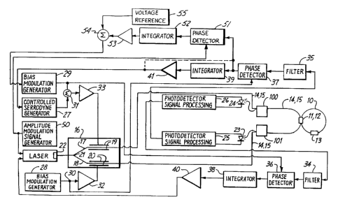
For instance, the systems shown in Figures l and 2 are often termed
"transmissive"
25 resonator fiber optic gyroscope systems. A "reflective" resonator fiber
optic gyroscope
system is another alternative which is shown in Figure 3, and in which the
optical Ken
2:~.~t~~Q~
WO 95!24611 PCTIUS95/02908
-29-
effect rotational rate is again reduced or eliminated by use of essentially
the same error
reduction system.
The major difference in the "reflective" resonator fiber optic gyroscope
system is
that there is but a single coupler optically connecting resonator 10 with the
remainder of
.5 the system. That is, a coupler designated 11,12 is shown in Figure 3 which
couples
electromagnetic waves into resonator 10 from, and out of resonator 10 to, an
external
optical fiber designated 14,15, serving as both the input optical fiber and
the output optical
fiber for the system. This is possible because of the use of two further
optical couplers,
100 and 101, which couple electromagnetic waves from external optical fiber
14,15 to
photodetectors 24 and 23, respectively.
The outputs of these photodetectors are provided to corresponding
photodetector
bias and signal processing circuits. 26 and 25, respectively. Photodetector
bias and signal
processing circuits 26 and 25 then provide signals to the same kinds of
feedback loop
arrangements in Figure 3 as similarly designated photodetector bias and signal
processing
circuits do in the systems of Figures 2A and 2B.
Again, the input signal for phase sensitive detector 51 can be taken as the
output
signal of phase sensitive detector 37 as shown in solid lines in Figure 3, or
that input
signal can be taken from the output signal from integrator 39 or amplifier 41.
Here too,
the example of taking the input signal for phase sensitive detector 51 from
the output of
amplifier 41 is shown in dashed line form.
Once again, the output signal of phase detector 51 is supplied to integrator
52
wherein it is time integrated and supplied to amplifier 53. Summing means 54
again
obtains the time integrated signal from the output of amplifier 53 and
combines it with a
signal from voltage reference 55 to supply the combination to the amplitude
control input
2'_> of bias modulation generator 29'. Once again, this added feedback loop
just described
provides the reduction or elimination of errors due to the optical Kerr effect
in the same
manner as done in the corresponding error control feedback loop shown in
Figure 2A.
The major difference in operation here is that the electromagnetic waves
reaching
photodetectors 23 and 24 are not only those waves which have been circulating
in
3(1 resonator 10 but also corresponding portions of the input electromagnetic
waves which are
not coupled into resonator 10 by optical coupler 11,12. Thus, there are two
pairs of
electromagnetic waves in external fiber 14,1 S with each member of each pair
following a
CA 02184496 2000-06-14
WO 95124611 PCT/US95l0290a
-30-
different path than the other, and with each pair reaching a corresponding one
of
photodetectors 23 and 24. This leads to each pair member interfering with the
other in that
pair in impinging on the photodetector corresponding to that pair. That is,
the electric
field components of the electromagnetic waves reaching photodetector 23 can be
represented as:
Ed-23 - ~l9Ein '+' c2Eccw
where Ed_z3 represents the electric field component of the electromagnetic
waves reaching
photodetector 23, qE'" represents the input electromagnetic radiation provided
through
integrated waveguide 17, E~~W represents the counterclockwise electromagnetic
waves
which have been coupled back into external fiber 14,15 from resonator 10, and
constants
c, and c, represent the effects of various fractional couplings, losses. and
phase delays on
these electromagnetic wave components reaching photodetector 23.
Similarly, the electric field components of the electromagnetic waves reaching
photodetector 24 can be represented as:
Ed -24 - ~3PEin + ~4 Ecw
with Ed_24 representing the electric field component of the electromagnetic
waves reaching
1 ~ photodetector 24, pE'" representing the electromagnetic wave electric
field component in
external fiber 14,1 ~ provided through integrated waveguide 18, E~W
representing the
clockwise traveling electromagnetic waves which have been coupled back into
external
optical fiber 14.15 from resonator 10, and constants c3 and c4 again
representing various
fractional couplings. losses and phase delays on these electromagnetic wave
electric field
components reaching photodetector 24.
Because the electric field components from two different optical paths in the
electromagnetic waves reaching photodetectors 23 and 24 will interfere with
each other
upon arrival, the intensities at these detectors must be written as
Id-Z3 - Ed-23' Ed_o3 -~~l9Ein~2~'~C2 Eccw~2+ ~icl qEinII c? Eccw~~osa'1
as
Id_24= Ed-24'Ed_y-~~3PEin~~~'~C4Ecwi2'+' ~~C3PEin~~c.tEcwicosao
WO 95124611 ~ ~ ~~ ~ ~ ~ ~ PCT/US95/02908
-:31-
with a being the phase difference between the components of the
electromagnetic waves
from two paths reaching a corresponding photodetector. As a result, the
equations
characterizing the system of Figure 3 will differ somewhat from the equations
given
previously characterizing the system of Figures 2A and 2B. In fact, the
occurrence of
resonance in resonator 10 leading to a peak in the electromagnetic energy
therein at the
frequency given such resonance will lead to a cancellation at the
photodetectors in Figure
3 so .that resonance is represented by a null in the intensity impinging on
those
photodetectors. Nevertheless, an analysis of the system of Figure 3 taking
these
differences into account will yield equations showing a similar result for the
optical Kerr
effect rotational rate error. Thus, a similar error reduction arrangement can
be used with
the system of Figure 3 as was used with the system of Figures 2A and 2B.
As described above, the system shown in Figures 2A and 2B, and in Figure 3.
succeed in eliminating the optical Kerr effect error through adjusting the
amplitude 0(3" of
the bias modulation signal at frequency f~ in a further feedback loop. This
loop is
1 _'i established by adding another phase detector at the output of the phase
detector following
the corresponding photodetector obtaining a signal from coil 10, with the
resulting loop
operating the corresponding bias modulation generator as the loop actuator.
Although
such a feedback loop has been shown to achieve the desired goal of eliminating
the optical
Kerr effect error, there are other error sources in coil 10 which have been
found possible to
reduce or eliminate by also adjusting the amplitudes of the bias modulation
signals. One
such example is the occurrence of errors due to backscattering of
electromagnetic waves
propagating in the optical fiber material of resonator 10 due to fluctuations
in the
refractive index along the propagation path therein due to splices, impurities
or minute
cracks all of which can leave such waves being reflected to travel in the
opposite direction.
2 '_,
Thus, to avoid conflicting demands on the bias modulation signal amplitudes,
there
is an advantage to canceling the optical Kerr effect rotation rate error by an
alternative
method at least in some situations. Such an alternative is available by
modulating the
electromagnetic waves directly in integrated optics chip 16 by providing
another signal to
3(1 the phase modulators in that chip or by adding a further phase modulator
therein to receive
that signal. The additional signal for this supplemental modulation can be
provided by a
controlled sinusoidal signal generator to thus introduce a further frequency
component into
2184495
WO 95124611 PCTIUS95102908
-:32-
the electromagnetic waves. If, for instance, an added phase modulator provided
in
integrated optics chips 16 is positioned about integrated waveguide 17, the
input
electromagnetic wave to resonator 10 from that waveguide will then have an
instantaneous
electric field frequency of
:) f0 +J 1 -fn ~~n Sln(~nt S- f~~b lnCUbt
wherein fb is the added frequency from the supplementary controlled sinusoidal
generator,
and Oc~b is the amplitude of this supplementary bias modulation phase change
at frequency
of fb. The frequency fb should be of a value that is large compared to the
frequencies of the
output signals from any of the other signal generators in the system of
Figures 4A and 4B,
sufficiently large so particularly that several cycles of this sinusoidal
signal are completed
during each cycle of the bias modulation signals fm and f" so that it appears
effectively as
an average value during such cycles. Such an introduction will change the
effective
propagation "constant" (3~~~,, in coil 10 to
~~~.,~ - ~o-~ - ~~nsln(D~t - ~~bsimwbt,
1 '~ where
~~b- C -fb~~b
Such a system is shown in Figures 4A and 4B. Again, designations used for the
various devices, transmission paths and blocks in Figures 4A and 4B are the
same as those
which were used in Figures 1, 2A and 2B for corresponding items shown there.
Rather
than the output of summing means 54 in Figure 2A going to the amplitude
control in bias
modulation generator 29' as shown in that figure, the output of summer 54 in
Figure 4A
goes to the amplitude control input of a supplementary sinusoidal output
compensating
generator, 60, shown in Figure 4B. The output of this compensating generator
is in this
last figure connected to added phase modulator 19' in integrated optic chip 16
(rather than
providing for an option of having the bias modulation generator 29 signal
being applied to
that phase modulator as indicated in Figure 2A). The bias modulation generator
in Figure
4A has again been designated 29 since there is no longer an amplitude control
input used
therewith.
21~:~Q~~
WO 95124611 PCT/US95/02908
-:33-
The introduction of this compensating signal through waveguide 19' changes the
behavior of the counterclockwise electromagnetic waves in coil 10. Although
the
intensity of these waves can still be written as:
Iccw(t~z) - Eccw'Eccw ~t~~P2Ene a~L zJ
x ~ for Il<zSL
(1- R )Z + 4R sin' ~ ~ccw + a xccw
2
and
(l~z) - ~t~2(1-Y2)(1-kz)P2E,e-°'~L-'~
Iccw
x I foro__<z<_ll,
(1- R )2 + 4R sin2 ~ ~ccw+ a Kccw )
2
the expression for the total phase change of the counterclockwise wave over
the optical
path through resonator optical fiber coil 10, D~~w except for the phase change
due to the
Kerr effect now becomes
~ccw ~ Np-IL - D~nLSInCO~t - D~ibLsinn~bt - ~r + 6.
As a result, the time average change in phase in the clockwise and
counterclockwise
directions from resonance set by the bias modulation feedback loop becomes
Occw--~l~[p2r(~~nsinwnt+0~3bLsinc~bt)+2q2r(~(3mLsinw",t),.
Similarly, for the clockwise wave, the corresponding average becomes
~cx,=-81p[qt r(0(3m Lsinc~mt)+2 p''r(O~in Lsinc~nt+8(3b Lsinwbt)].
As a result, the initial expression for the rotation rate error due to the
optical Ken effect
based on these quantities becomes
I p [q2 r(~ (3m L sinw mt) - pZ I~'(0 (3n L sin w nt + ~ ~3b L sin w bt),.
The two time averages occurring in this last expression for the rotation rate
error
1 _'s due to the optical Kerr effect are evaluated as
WO 95124611 PCTIUS95102908
-34-
r(0 (3n L sinw"t + ~(3b L sinwbt)
W J _1
T o 1 + R2 -2Rcos(0 (3n L sinw "t + ~ (36 L sinwbt J dt
_ 1 RD ~3n L2 Rr, ~3b L2
=(1-R)2-2(I-R)a-2(I-R)a
I R(0 ~3n + D ~9) L2
(1 _ R )2 _ 4,(1 _ R )a
and
T
r(0(3mLsinwmt)= T J I+R2=2Rcos(0(3mLsinwmt)dt
1 Rd (3m L2
-(I-R)2-2(l-Rya
These results can be rewritten if the definitions
~~n+~~b,
~Q D~3m+~(3r~
- 2
and
~ ~m ~ ~r
2
are made. Then, each time average becomes
r(~~3nLsinwnt+p~36Lsinwbt)- 1 RL2~~2 RL2~~0~0
(1-R)2-2(1-R)a- (1_R)a
and
I-' D Lsinw t = 1 RL20(~2+RL2~~0(~0
( ~m m ) (1-R)2-2(1-R)a (l-R)~i
WO 95!24611 ~ PCT/US95102908
-35-
Substituting these results for the time averages into the preceding expression
for
the rotation rate error due to the optical Kerr effect yields
_ ~,c q2 _ p2 _qZRO(32j,'' p2R~/32L2
8~qsj° (j_R)2 (j..R)Z 2(j_R)Q 2(j_R)4
-q2 R~~O ~Q L? p2 R~~O ~Q Lz
(j-R)4 __ (j-R)a
Algebraic manipulation yields
_ ~,.c81o~2(j-R)2-R~~2L2~ (q~-P2)-(q2+PZ)- 2R0(3L2
eke 16T<.4(1-R)4 2(1-R )2-R~(32L2
Making the definitions
~,c8(2(I-R)2-RO(32L2J
j6~,4(I -R)4
and
R0~3L
C202(1_R)2_R0~2L2
this rotation rate error becomes
eke -Cllo~(q'-PZ)-C2(~~m'~~r)L(P2+q1)~
This last expression is the same expression obtained above for the system of
Figures 2A
and 2B but with different definitions for constants C', and C'z then there
were for
constants C, and CZ found for that system. In addition, 0~3r here replaces
O~i~ which
1 C) appeared in the earlier error equation for the system of Figures 2A and
2B.
Hence. once again, rotational rate error due to the optical Kerr effect is
seen to
depend linearly on the input intensity of the electromagnetic waves provided
by laser 22.
As a result, also again, any change occurring in the optical Ken effect
rotation rate error
because of a corresponding change in the input intensity will also be linearly
related.
1 ~~ Thus, if the same amplitude modulated electromagnetic wave intensity from
laser 22 is
provided by amplitude modulation signal generator 50, the relationship between
the
2~.~~~~
WO 95124611 PCT/US95I02908
..36_
change in output error due to the optical Kerr effect in the amplitude
modulation can again
be found in a frequency component at modulation frequency f~, as seen from the
resulting
expression
~52~ =Cj~~Rz'P2~'C2L~P2+92~~~~m- O~n+~~h ylamcosc~I
where the substitution
~~r ~~n+O~b
has been made. Once again, the relationship between the change in intensity
and the
optical Ken effect error is seen to depend in part on a parameter which can be
controlled,
O~ib, which differs from the bias modulation amplitudes ~~3m and D(3". As a
result, the
output error due to the optical Kerr effect can be substantially reduced or
eliminated by
driving toward zero the amplitude modulation component at frequency of a",
that is present
in the bias modulation signal amplitude at frequency f" obtained from
photodetector signal
processing circuit 25 as before, through filter 35, phase sensitive detector
37 and phase
sensitive detector 51. The feedback loop containing these components again has
the error
signal provided at the output of phase detector 51 to be used to adjust the
supplementary
modulation amplitude O~h in such a manner to drive this error signal to a
value of zero in
view of the presence of integrator 52.
The output signal of phase sensitive detector 51 is found as before, but using
instead the expression just obtained for the change in the optical Kerr effect
error due to
the output intensity of laser 22 being amplitude modulated, yielding
V5~ = Gram C1~~92-P2~-C2L~PZ+9Z~~D~,n- ~~n+~~b~~
If the signal vsl is forced to zero, that is, v_;~ = 0, the resulting
expression is obtained for
the supplementary modulation amplitude
~q2 P2~ ~ ~n.
0~6= O~m_C2L~P2+92~
PCTIUS95I02908
WO 95124611
-37-
This value for ~(3b can be shown to force the error due to the optical Kerr
effect to zero.
Thus, the supplementary feedback loop involving phase sensitive detector 51,
integrator
52, amplifier 53, compensating generator 60 and phase modulator 19' also
permits
substantial elimination of the error in the rotational rate information due to
the optical Kerr
effect.
Figure 5 shows a reflective resonator fiber optic gyroscope system which uses
essentially the same error reduction system as was used in the transmissive
system of
Figures 4A and 4B. Except for this error reduction system, the system of
Figure S is
substantially like the system of Figure 3.
Although the present invention has been described with reference to preferred
embodiments, workers skilled in the art will recognize that changes may be
made in form
and detail without departing from the spirit and scope of the invention.