Note: Descriptions are shown in the official language in which they were submitted.
Rechts-~Pntent8nwnltKll~ugl1ierswn '~9621656001 ~6.08.19S6 ~ S~ Uhr ~5/9
~184~6 '
T R ~ N S ~. A T I O N ,l ~ t -, .
Technical objective:
The invention relates to a chip card with several vwlli~ullers as well as
5 cnnn~ctir)ne for data exchange with read/write devices, whereby thc
are contact ~nnnH~tinnc as we~l as contact-free .. IH I ~- -e and the
read/write devices are capable of accessing the various microcontrollers
D~ ly, according to the generic part of Claim 1.
10 State of the art:
Plastic cards are known as chip cards which ex( hangc energy and data with
their read/w~te devices with or without contacts. These cards aro used for
nu}nerous Arr~ tinnC such as, for example, telephone cards, medical cards,
access control cards. A chip card of tbis type is known from G~n patent no.
15 393S364 C1.
German patent no. 91 00 861.9 U1 discloDes a data ca~rier e~hange arrange-
ment that has a first Illi~_lV~V-,~DDV~ with first contacts arranged according to
T"~. "~.imlaI Oi~.,; al: .,. for St~:Lda~liL~lion (ISO) Standard 7816-2 (Part
20 2); The data carrier exchange arrangement has at least a second micropro-
cessor with second contacts whose arrangement on the data carrier exchange
arrangement does not cu..~D~ulld to the ISO Standard. This data carrier
eschange arrAngannPnt can have cvntact, --.-,-~. I ;.,..c as well as contact-free
~,"---~ Il,,.,~
Te~ical objective:
The invention is based on the objective of ~ae~ .; ,.g various card Arp~ atinne
which am eYecuted at a terr~inal (read~write devioe) using cards with various
~vw-~ vllers on the chip card.
Disclosure of the invention and of its advantages:
The objective is achieved accvrding to the invention in that the 1l .. -- l~ 1 l. ll l~ are
each made to a mnn~rt;ng unit which is either a separate electrvnic
.~ ....l~ ...~, .I or els~ is illl~ L~d into a ~ llLilll.Al ' ~v .L~vller and which,
35 on the basis of the ;nfm rn~tinn available at one of the cnnn~;nne or on the
basis of the physical cvnfiguration of the . -IIIH I i-~--e, decides which of the
mi,.v.vLl~.vllers should enter into the data exchange with the read/write
Rechts-LPotsnto~woltKloustlierswD ~456~1856001 ~16.08.1996 ~ 52Uhr D6~9
~ 218~606
. - ~
device, and in that the 1l ", .. I l r ,g unit f~Ct~hli ehf c a c. ,....,~ - . for the clata
exchange ~etween the ~, .. ~ 1 ;- ,. ,c and the ;~w L~illillg ~ lu~ullLlvller~
In an adv;~ manner, the .. ,... If ~ unit is either a separate ele~tronic
5 ~ . or it is i..Le~ldL~ d into a conventional r.l.~lu u~ vller. Moreover,
the f~ I; r .g unit uses the physical cvnfiguration of the contact f.... r .~ ... C
and/or of the contact-free cnnn.ortif,ng to recognize which of the micro-
c~trvllers should enter into the clata exchange with the read/write device.
10 Ihe evaluation of the physical rvL~ ul dLiull of the co~tæt cnnnP~ t.inne ancVor
the contact-free cnnnfct;f~ng can be carried out by signal tr~ncmi~inn by
~ ~ . ,n . . ~ cvntæts on the chip card.
Ihe ~ ~ - - r- I; r g unit, which can be referred to as a Combi Interfæe Chip (CIC),
15 is arlv~ u- ~ly a f.. .~Y...~..I. which, as a ~ . to a ~u~ul~L~ullf-r~
can be u~ed on chip c-~s or, with its functions æcording to the patent, can be
illLe~ld~d into a rvllv~lLiuLIal card controller. In an adv~rl~ff)ll~ manner, bymeans of the fnnnf fti~n unit, it is possible to use a card at a terminal for an~lif~tinn A which rf~quires the ~,i~u~ull~vller A as well as at a terminal for
20 an :lrrlifsltinn B which requires the ~u~ul~ ler B.
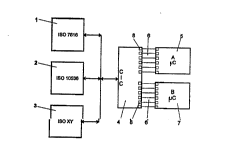
Brief fif cfri~i~m of the drawings in which thf~ following is shown:
Figure 1 schematic view of the various n nn~tinnc 1, 2, 3 to readlwrite
clevices outside of the chip card, in which the ~, .... ,f I; ..g unit is
installe~ dirf~ctly cln the chip of a ,. i~u u-.LIvller and
Figure2 another~...l~1;...~..1.ofa..,..1.,~1;r.gunitinnonil.Lt,~ldL~dform,
whereby there are contact surfæes which allow the . . ., - IH I " 1l l of a
first Illi.l u~ullLI uller and of a second LUi.l u.~.lLI uller.
30 Ways to execute the invention:
Figur~ 1 is a schematic view of the variou fnnnf~cff~nq 1, 2, 3 to reacVwrite
clevices outside of the card. In their va~ing physical configurations, these
;- " ,c a~ made to a, ~ .... IH I r g unit 4. Ihe ...~ I r .~ unit 4 makes the
various Cnnnfrtinng 1, 2, 3 in a uniform fnnnfrtinn 6 available for the
35 fnnnfY ti~n of ~flfli ffnn~l chips. The f. ~ I . r .g unit 4 is installed c~irectly on
the chip of a mi..~L~ller 5 (A5p) (i~lL~I dL~d solution).
Re~his-t~Po~eT~tonwoltKlousr1ierswr2 ~t4g62las600~ 60a~ss6 ~1~s2uhr D7fg
7 21 8~6~
On the basis of the physical conflguration of the rnnnPrtinne or of thei.l~'~.. ':".availableatthe.~...,.al;...etoareadfwritedevice,ther..,..,~;..g
unit 4 must decide which .. L..U~Ul.LLUIler on the card is to be used. If, for
example, the inffirrn~hnn coming from the readlwrite device indicates that
5 mi~l ~u~lLuller A is not meant for the task in question, the ~ . 1 of the
incoming information is switched over from this LLli~lu vllt.luller to another
r~P~ ,.. 6 which is available for another .. lu~ullLLuller. The incoming
infnr~nr~tinn can be evaluated by soP~ware in the .~1..r,a 1~"g unit 4 ~ if the
.~..."r~l1;..~unit4isronfiguredasa~lu~lu~ ul ~orbyahard-wiredlogic
circuitonthe.. "H l;~.gunit4.
Figure2showsanotherr~mholimPntofther....... ~l;r.gunit41ikeinFigurel,
but in a nonill~;l dLrdd form. In addition, contact surfaces 8 can be seen whichallow the rnnnpcti~n of a first mi.lu~u,,Ll-uller 5 (A5C) and of a second
15 ,.- Iu~u,,LL~ler 7 (B5C).
The function of the r.. ,~ I 'r,g unit 4 cdn be carried out on a chip car~ as aseparate comrnnpnt~ whereby contacts 8 are available for this purpose.
However, the function can also be illLr~L~d into a l"i.,u~u.,L,~dler 5 so that
20 this ,~ lu~u~Ln~ller 5 can also take ovPr the evaluation of the infnr~n~tl~n from
the readlwrite drvices.
Ihe physical configuration of rnnnPrtinne 1, 2, 3 also allows for a dPcision as to
which mi~u.u,,Lluller 5, 7 is to be used. If, for example, coils or cnnrlr~nePr
25 surfaces have been activated for a contact-free tr~nrmir~;nn it is likewise
possible to switch over to a specific c - ,. .f~ I , 6.
Contact card fields on cards accor~ing to ISO Standard 7816 and in read~'write
devioes ~, ." ,.-1; " ,.~ hav-e lmnr~lrir~l contact nnnPr~i,.ne In an advs nt5l~ue
30 manner, these can be used by means of a physical signal evaluation for a
L~ . .~ . of the ~ ,lir~ ., and thus for a ~w;l~l.uv~ in the c,.. ,,.H l ;r.~ unit
4. For this purpose, for example, a voltage must be applied to the contact
,~ " " ,~ I ;. .., c in the read/write devices.
35 Commercial sl~lir~hility
The subject matter of the invention can be used for chip cards, especially
plastic cards, fûr puIposes ûf datd eschange in ~ ,v.LL~ devices. Such ~hip
cards, which can eschange energy and data with read/write devices with or
, . . , .,, . . . . .. . ,, .. ,. ,.. ,, , .. . , . . ,. .~ = ~ ~ , .... .... . . .
Rechts-~PstentsnwoltKI8u5t1~er5w8 ~r~4962~856001 ~11608.1996 ~lt:s3uhr ~8/9
.
"~ ~18qCQ6
w~thout oontt~cts, are a~v~n~og~l~ly used for telep;hone car~s, medical cards
or t3ccess control ct3r~s.