Note: Descriptions are shown in the official language in which they were submitted.
CODE DIVISION MULTIPLE ACCESS MOBILE COMMUNICATION SYSTEM
The present invention relates to a mobile
communication system operating on what is known as the
code division multiple access (CDMA) system.
The CDMA system involves multiplexing a plurality
of communication channels using spread spectrum codes,
each channel being assigned a different spread spectrum
code. A given signal to be transmitted is multiplied
(i.e., spread) by the spread code assigned to its own
channel, and is multiplexed with other similarly spread
signals on different channels before being transmitted.
At a receiver, the multiplexed signals are multiplied
(i.e., despread) by the same spread code so that only
the target signal will be extracted correlated on its
own channel. The signals on the other channels are
perceived merely as noise because these signals with
their different spread codes remain uncorrelated. The
~°_ 1 _
~lg'l9-~g
level of the noise can be sufficiently lowered so as not
to disturb the signal reception. The CDMA system is
attracting attention as a system fit for drastically
improving the efficiency of frequency utilization and
has been commercialized in some areas.
Where CDMA communication is implemented using
spread codes, some kind of signal modulation (e. g.,
quadrature phase shift keying or QPSK) precedes the
spreading of the signal for transmission. At a
receiving point, the despreading of the signal is
followed by demodulation. Despreading and demodulation
both represent the detection process whereby the
transmitted signal is reconstructed. Commonly used
detection methods include a coherent detection method
based on a PLL (phase locked loop) circuit and a
differential detection method. There also exists a
recently proposed coherent detection method that
utilizes pilot signals.
Where the CDMA system is applied to a mobile
communication system adopting the conventional coherent
detection method, the bit error rate of data in a mobile
station deteriorates if fading occurs while the
station is moving. In a CDMA mobile communication
system utilizing the differential detection method, the
A
~i84°~~
bit error rate of data in a mobile station can worsen
due to the noise on the air transmission channel even if
the station is stationary. The pilot signal-based
coherent detection method has been proposed for a system
to minimize the deterioration of the bit error rate
whether the mobile station is in motion or at rest. The
method was discussed at the Autumn 1994 Symposium of the
Institute of Electronics, Information and Communication
Engineers of Japan as disclosed in the IEICE collection
of papers B-5 on radio communication systems A and B, p.
306, "Coherent detection for CDMA Mobile Communication
Systems" by Yasuo Ohgoshi et al.
Described below is a conventional mobile
communication system that uses pilot signals with
reference to the above-cited paper supplemented by some
details. The description will first center on the down
link of the system (i. e. , a link from the base station
to a mobile station). FIG. 13 shows a modulation
circuit 51 of a base station 1 that transmits data and a
first half 52 of the detection circuit of a mobile
station 2. The base station 1 actually transmits
signals to a plurality of mobile stations 2, and FIG. 13
shows one station as the representative example.
In the modulation circuit 51 (left-hand half of FIG.
-3-
218493
13), data first undergoes QPSK modulation, not shown, to
divide into an in-phase signal I and a quadrature signal
Q. The signals I and Q are spread (i. e. , multiplied)
respectively by spread code signals PN_ID and PN_Qp.
The two spread code signals are supplied from a spread
code generator 91. The rates of the spread code signals
PN_ID and PN_QD (called the chip rates) are used to
multiply by k (k: spreading ratio) the pre-spread rates
(called the symbol rates) of the signals I and Q so that
the latter will attain the chip rates. The signals thus
spread pass through a radio frequency quadrature
modulator 54 to become mutually perpendicular signals
that are transmitted on a radio frequency band from an
antenna. A temperature compensated crystal oscillator
61 is provided to furnish the modulator 54 with a
carrier CB.
The pilot signals will now be described. The
transmission circuit is substantially the same as the
left-hand half of FIG. 13 and is omitted. An in-phase
signal Ip and a quadrature signal QP of the pilot '
signals are spread respectively by spread code signals
PN_IP and PN_QP. Both spread code signals have the same
chip rate as in the case of data. The pilot signals
thus spread are subject to radio frequency quadrature
-4-
modulation by the same carrier CB as with data, turning
into mutually perpendicular signals transmitted on the
same radio frequency band as with data. The pilot
signals serve as reference signals for demodulation and
are common to all channels utilized.
In the first half 52 (right-hand half of FIG. 13)
of the detection circuit of the mobile station 2, the
received signals from the antenna (data and the pilot
signals) pass through a radio frequency quadrature
demodulator 57 to reach a low-pass filter 56. The low-
pass filter 56 removes the radio frequency components
from the signals to yield signals SI and SQ. A crystal
oscillator 60 supplies the demodulator 57 with a carrier
CM. The signals SI and SQ are composed of the spread
signals I and Q (those destined to their own channel as
well as to other channels) and of the spread pilot
signals IP and Qp . As such, the signals SI and SQ
include a phase error caused by fading and a frequency
error attributable to the precision of the oscillator 60.
The errors included in the signals SI and SQ
produce a phase difference therein. When the mutually
perpendicular pilot signals are plotted in orthogonal
coordinates, the received pilot signals are rotated
exactly by the phase shift, as shown in FIG. 14. If the
A
-5-
_ 2184938
phase shift is represented by ~ and the orthogonal
coordinates after quadrature demodulation are designated
by X1 and Y1, then the coordinate axes X and Y of the
received signals are rotated by ~ displacing the pilot
signals. Consequently, the undisplaced signals i and q
that should have resulted with no phase shift become il
and ql respectively. Such changes are caused by the
mixing of one of the two mutually perpendicular signals
into the other signal. The phenomenon is expressed by
the following formulas:
il - icos~ - qsin~
q~ - qcos~ + isin~
The pilot signals are signals that stay constant
following the despreading. Generally, i - 1 and q = 1.
The signal changes into il and ql permit acquisition of
a signal CS with the value cosh and a signal SN with the
value sink. With the two signals known, it is possible
to correct the phase rotation of the data. Since the
data includes the same phase shift, the despread data
signals are inversely rotated by ~ using the signals CS
and SN whereby the initial signals I and Q are correctly
reconstructed. Thus the signals CS and SN serve as
phase correction signals.
The signals SI and SQ output by the first half 52
-6-
~i~~~
of the detection circuit are subject to despreading and
phase correction by the second half of the detection
circuit shown in FIG. 15. A pilot signal despreading
unit 21 in the upper left portion of FIG. 15 despreads
the signals SI and SQ by use of the spread code signals
PN_IP and PN_QP from a spread code generator 25, whereby
the pilot signals are extracted. The extracted pilot
signals are then added and subtracted mutually, becoming
a signal CSC with a chip rate of cosh and a signal SNP
with a chip rate of sink. The two signals are converted
to the symbol rates by an accumulator 41 and thereby
turn into phase correction signals CSS and SNS of the
preliminary stage. The phase correction signals are
averaged by an averaging circuit 43 for noise reduction.
The averaging provides the phase correction signals CS
and SN of the final stage.
FIG. 16 shows a typical circuit constitution of the
averaging circuit 43. Reference numerals 430 through
433 are delay gates (Ds) for delaying a signal by a one-
symbol period each. In this example, three consecutive
symbol values are averaged when added up by adders 235
and 236. It is through this noise reduction arrangement
that the phase correction signals CS and SN are obtained.
The delay time (average delay time) T required for the
~ / g~ 93 ~
averaging by the averaging circuit 43 is given as
T = Ds X (N - 1) /2
where N denotes the number of symbols used for the
averaging operation.
The data signals SI and SQ are both despread by an
inverse data spreading unit 42 (bottom left in FIG. 15)
using the spread code signal PN_ID for the signal I and
the spread code signal PN_Qp for the signal Q. The
operation causes four signals to be extracted. The four
chip rate signals are converted by an accumulator 44
into symbol rates to become signals D1 through D,.
After this, the signals D, through D4 are each delayed
by a data delaying unit 48 (FIG. 17) by the average
delay time T of the averaging circuit 43. The operation
yields signals Dlo through D<o. Where the data delaying
unit 48 is constituted by a number of delay gates (Ds)
in stages of cascade connection each gate providing one-
symbol period delay, the gate count M per stage is given
as
M = (N - 1) /2
In the above example, N = 3 and thus M = 1, so that the
delay gates 480 through 483 of the data delaying unit 48
are each composed of a one-symbol delay gate (Ds).
The signals Dlo through D4o are fed to a phase
_g_
218493
correction circuit 49 in which the signals are corrected
in phase rotation by use of the correction signals CS
and SN. A typical constitution of the phase correction
circuit 49 is shown in FIG. 18. The phase correction
circuit 49 performs phase correction as follows: the
signals Dlo and D4o are multiplied by the correction
signal CS, and the signals DZO and D3o by the correction
signal SN. The multiplied results are added and
subtracted mutually so as to rotate the orthogonal axes
of the received data by -~ in phase (i.e., the phase
shift ~ is reduced to zero in FIG. 14). The phase
correction provides reconstructed signals IR and QR of
the original signals I and Q. The signals IR and QR
then undergo QPSK demodulation, not shown, to become the
original data.
One disadvantage of the conventional detection
circuit above is that the restored signals IR and QR are
unavoidably affected by the frequency precision of the
crystal oscillator 60 (right-hand side in FIG. 13). A
transmitter 60 used in the mobile station necessarily
includes a certain practical frequency error because the
mobile station is f or use by general users. That is, on
the one hand, if the frequency error involved in the
data is large enough to cause apparent phase
_g_
~~ $~~~g
irregularities over the average delay time T during data
demodulation, no precise correction signals can be
acquired and the bit error rate of the detected data
worsens. On the other hand, if the average delay time T
is shortened to avert the deterioration of the bit error
rate, the adverse effects of the frequency error are
diminished but the line noise becomes more pronounced.
On the up link (i. e. , a link from the mobile
station to the base station), the carrier CM from the
crystal oscillator 60 often doubles as a carrier for use
in radio frequency quadrature modulation by the
modulation circuit of the mobile station. In that case,
the signals transmitted by the mobile station and
received by the base station include both the phase
error caused by fading and the frequency error
originating from the crystal oscillator. The frequency
error results in the inevitable deterioration of the bit
error rate in the detection process of the base station.
The deficiencies above are conventionally
circumvented, particularly where data of lower bit rates
than normal are transmitted, by the method of burst data
transmission with no change in the spreading ratio, as
stipulated by the U.S. digital radio communication
standard IS (Interim Standard)-95. Under the system,
- 10 -
2 ~ ~.~~
transmitting data at 1/r of the standard bit rate
compresses the data to 1/r in temporal terms. The time-
compressed data is transmitted in bursts at fixed
intervals.
How the burst signals are sent intermittently is
illustrated in FIG. 19. In FIG. 19, the axis of
abscissa represents time and the axis of ordinate
denotes transmission power. Reference numeral 140 is a
radio signal waveform of standard bit rate data.
Reference numerals 141, 142 and 143 stand respectively
for radio signal waveforms of data at 1/2, 1/4 and 1/8
of the standard bit rate. The number of burst signals
varies with the bit rate. All burst signals have the
same standard bit rate when temporally compressed as
described. It follows that every burst signal has the
same symbol rate and thus the spreading ratio remains
unchanged.
The arrangements above are necessitated by the
following reasons: if compression is not carried out,
the one-symbol period gets longer the lower the data
rate. Meanwhile, the number of symbols N for use by the
averaging circuit 43 (FIG. 15) in the demodulation
circuit remains substantially the same regardless of the
bit rate in view of noise reduction. Thus the average
- 11 -
~C.~ ~,~''
J
delay time T becomes longer the lower the data rate. A
prolonged delay time T prompts the frequency error to
deteriorate the bit error rate as discussed above. The
lower the bit rate, the more deteriorated the bit error
rate. To avoid this deficiency requires keeping the
symbol rate constant. The requirement necessitates the
use of complicated circuits in the mobile station, which
runs counter to the inherent need for the mobile station
to simplify its circuitry.
It i's therefore an object of the present invention
to overcome the above and other deficiencies and
disadvantage of the prior art and to provide an improved
CDMA mobile communication system permitting stable
signal reception with a minimum of bit error.
In carrying out the invention and according to one
aspect thereof, there is provided a CDMA mobile
communication system including a mobile station
comprising a voltage-controlled oscillator and a
frequency controller. The voltage-controlled oscillator
acts as a circuit to supply a carrier to a radio
frequency quadrature demodulator. The frequency
controller detects a frequency error from a phase
A
- 12 -
correction signal of the first step and uses the
detected frequency error as the basis for generating a
control signal for use by the oscillator. The frequency
controller may illustratively be composed of two
circuits: a circuit for detecting a phase change caused
by the frequency error derived from the phase correction
signal of the first step and from a signal preceding the
correction signal by a predetermined delay time; and an
integrating circuit for integrating the phase change and
outputting the result as the above control signal.
The voltage-controlled oscillator and the frequency
controller operate to establish within the detection
circuit of the mobile station a control loop whereby the
phase change is reduced substantially to zero. This
minimizes the frequency error. Because the frequency of
the oscillator is kept as precise as that of the
oscillator of the base station, the phase shift
attributable to the frequency error is significantly
reduced. This provides a detection circuit that works
stably with a minimum of bit error.
The predetermined delay time may preferably be set
within a range not exceeding the delay time needed for
the averaging operation by the averaging circuit which
admits the phase correction signal of the first step and
- 13 -
outputs a phase correction signal.
The carrier to a radio frequency quadrature
modulator may preferably be supplied by the voltage-
controlled oscillator. Because the frequency of the
radio signal sent to the base station is kept accurate,
the base station is allowed to implement pilot signal-
based coherent detection stably with a minimum of bit
error. Where the mobile station transmits data at a low
bit rate, the system allows the terminal to keep the
chip rate of the spread code constant and to transmit
data with varying spreading ratios but without time
compression. Such data transmission is readily
implemented by changing the circuit constant in keeping
with the symbol rate of the data, with no change in the
circuit constitution.
These and other objects and many of the attendant
advantages of the invention will be readily appreciated
as the same becomes better understood by reference to
the following detailed description when considered in
connection with the accompanying drawings.
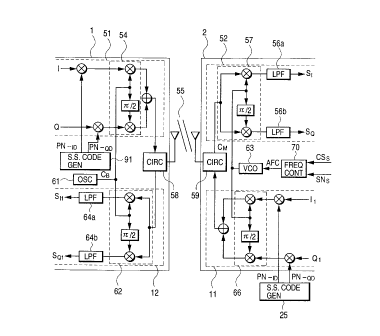
FIG. 1 is a circuit diagram of a CDMA mobile
communication system based on a CDMA detection circuit
P
~ ';- 14 -
ZZ ~~9~~
and practiced as a first embodiment of the invention;
FIG. 2 is a schematic view showing a pilot signal
as it is related to data in a signal transmitted by the
base station of the first embodiment;
FIG. 3 is a circuit diagram of the second half of
the detection circuit in a mobile station of the first
embodiment;
FIG. 4 is a circuit diagram of a frequency
controller used by the first embodiment;
FIG. 5 is a circuit diagram of another frequency
controller for use by the first embodiment;
FIG. 6 is a schematic view depicting a pilot signal
as it is related to data in a signal transmitted by the
mobile station of the first embodiment;
FIG. 7 is a circuit diagram of the second half of
the detection circuit in the base station of the first
embodiment;
FIG. 8 is a schematic view illustrating pilot
signals as they are related to data in a signal
transmitted by the mobile station of the first
embodiment;
FIG. 9 is a schematic view explaining data
transmission by the mobile station of the first
embodiment;
- 15 -
a
FIG. 10 is a schematic view showing a pilot signal
as it is related to data in a signal transmitted by a
mobile station of a second embodiment;
FIG. 11 is a circuit diagram of the second half of
the detection circuit in the base station of a third
embodiment;
FIG. 12 is a circuit diagram of a temporary judge
circuit in the second half of the detection circuit
shown in FIG. 11;
FIG. 13 is a circuit diagram of the modulation
circuit in a conventional base station and the first
half of the detection circuit in a conventional mobile
station;
FIG. 14 is a schematic view of a receiving point as
it is rotated in phase;
FIG. 15 is a circuit diagram of the second half of
the detection circuit in the conventional mobile station;
FIG. 16 is a circuit diagram of an averaging
circuit in the second half of the detection circuit;
FIG. 17 is a circuit diagram of a data delaying
unit in the second half of the detection circuit;
FIG. 18 is a circuit diagram of a phase correction
circuit in the second half of the detection circuit; and
FIG. 19 is a schematic view depicting data
- 16 -
-.~ i ~ 'i' 9 ~
s
transmission by the conventional mobile station.
Preferred embodiments of the invention relating to
a CDMA mobile communication system will now be described
in detail with reference to the accompanying drawings.
In FIGs. l through 12, the component parts with their
functionally identical or equivalent counterparts
included in the prior art examples of FIGS. 13 through
18 are designated by like reference numerals.
<First Embodiment>
FIG. 1 is a circuit diagram showing the overall
constitution of a CDMA mobile communication system
practiced as the first embodiment of the invention. The
base station, which transmits data usually to a
plurality of mobile stations, is shown sending data to a
single mobile station in FIG. 1. In the left-hand half
of FIG. 1, reference numeral 1 is a base station; 51 is
a modulation circuit; 91 is a spread code generator; 54
is a radio frequency quadrature modulator; 61 is a
temperature compensated crystal oscillator; 58 is a
circulator for separating a transmitted radio signal
from a received radio signal; 12 is the first half of a
A
- 17 -
detection circuit; 62 is a radio frequency quadrature
demodulator; and 64 is a low-pass filter. Reference
characters I and Q are an in-phase component signal and
a quadrature signal respectively; PN_ID and PN_Qp are
spread code signals for the signals I and Q respectively;
SI1 and SQ1 are an in-phase component signal and an
opposite-phase component signal, respectively, subject
to the spreading of the output of the detection circuit
first half 12; CB is a carrier output by the oscillator
61; and 55 is an air transmission channel.
In the right-hand half of FIG. 1, reference numeral
2 is a mobile station; 52 is the first half of a
detection circuit; 59 is a circulator for separating a
received radio signal from a transmitted radio signal;
57 is a radio frequency quadrature demodulator; 56 is a
low-pass filter; and 63 is a voltage-controlled
oscillator. Reference characters CM stand for a carrier
output by the oscillator 63, and AFC for a control
signal for controlling the frequency of the oscillator
63. Reference numeral 70 denotes a frequency controller
for generating the control signal AFC. Reference
characters CSS and SNS stand for phase correction
signals of the first step, to be described later; and SI
and SQ for an in-phase component signal and an opposite-
- 18 -
~18~9~~
phase component signal subject to the spreading of the
output of the detection circuit first half 52.
Reference numeral 11 is a demodulation circuit; 25 is a
spread code generator; and 66 is a radio frequency
quadrature modulator. Reference characters I1 and Q1
represent an in-phase component signal and a quadrature
component signal, respectively, of the data transmitted
by the mobile station to the base station; and PN_ID and
PN_Qp denote spread code signals for the signals I, and
Q1, respectively, output by the generator 25.
Described below is the case in which the base
station 1 transmits data and a pilot signal over a down
link to the mobile station 2. The modulation circuit 51
is substantially the same in constitution as its
conventional counterpart in FIG. 13. The data to be
transmitted passes through a QPSK modulator, not shown,
to become signals I and Q. The signals I and Q are
spread by use of the spread code signals PN_ID and PN_QD.
The spread signals are turned by the radio frequency
quadrature modulator 54 into mutually perpendicular
radio frequency band signals that are transmitted from
an antenna past the circulator 58. The temperature
compensated crystal oscillator 61 supplies the modulator
54 with the carrier CH.
- 19 -
Although not shown, An in-phase signal Ip and a
quadrature signal QP of the pilot signals are spread
respectively by spread code signals PN_IP and PN_QP.
Both spread code signals have the same chip rate as in
the case of data. The pilot signals thus spread are
subject to radio frequency quadrature modulation by the
same carrier CB as with data. Following the modulation,
the signals turn into mutually perpendicular signals
transmitted on the same radio frequency band as with
data.
FIG. 2 schematically shows a radio frequency band
signal transmitted by the base station 1. In FIG. 2,
reference numeral 92 is a radio frequency band signal
representing the pilot signal, and 93 is a radio
frequency band signal that carries data. Data 2 in the
signal 93 is destined to the mobile station 52; data 1
and p are directed to other mobile stations. The data
signals 1 and p are each spread by a different spread
code signal.
The data and pilot signals are thus transmitted on
the same radio frequency band and received by the mobile
station 2 (right-hand half of FIG. 1). The received
signals are fed to the radio frequency quadrature
demodulator 57 past the circulator 59. The output of
- 20 -
2~ 84~.~~
the demodulator 57, from which the low-pass filter 56
removes the spurious part, becomes the signals SI and SQ.
The voltage-controlled oscillator 63 supplies the
demodulator 57 with the carrier CM.
The signals SI and SQ are despread and phase-
corrected by the second half of the detection circuit.
This yields restored signals IR and QR originating from
the initial signals I and Q. FIG. 3 is a circuit
diagram of the second half of the detection circuit in
the mobile station. The output terminals of the
accumulator 41 are connected to the input terminals of
the frequency controller 70 which is fed thereby with
the phase correction signals CSS and SNS of the first
step. Except for these connections, the setup of FIG. 3
is the same as that of the conventional circuit in FIG.
15. The component parts having their functionally
identical or equivalent counterparts included in the
prior art examples will not be described further.
The oscillator 63 (in the right-hand half of FIG. 1)
is a known circuit using a variable capacitance diode
(not shown) as the element to determine the oscillation
frequency. The diode has its capacitance changed when
fed with the control signal AFC, whereby the oscillation
frequency is controlled.
- 21 -
The frequency controller 70 that outputs the
control signal AFC works as follows: a phase shift of Oq~
is detected as a phase change of about one-symbol period
stemming from the frequency error of the oscillator 63.
The sine component (sinOq~) of the phase shift is fed to
an integrator so that the latter will output the control
signal AFC. FIG. 4 shows the circuit constitution of
the frequency controller 70. In FIG. 4, reference
numerals 700 and 701 are delay gates (Ds) having a delay
time of one-symbol period each, 705 and 706 are
multipliers, 707 is a subtracter, 708 is a multiplier,
and 709 is an integrator.
The signals CSS and SNS are delayed by the delay
gates 700 and 701. The multiplier 706 multiplies the
signal SNS by a signal succeeding the signal CSS by one
symbol. The multiplier 705 multiplies the signal CSS by
a signal succeeding the signal SNS by one symbol. The
subtracter 707 subtracts the product of the multiplier
706 from that of the multiplier 705, yielding an error
signal SNO having a value of sinA~. If 0~ « n, then sin
A~ is approximately equal to 0~. The error signal SND
having the value of sine is multiplied by the
multiplier 708 to provide a predetermined loop gain.
The multiplied result is integrated by the integrator
- 22 -
709 that produces the control signal AFC.
The controller 70, oscillator 63 and radio
frequency quadrature demodulator 57 in FIG. 1 as well as
the despreading unit 21 and accumulator 41 in FIG. 3
constitute a control loop in which the integrator 709
integrates the signal SNP so that the latter will
approach zero. This arrangement inhibits the frequency
error and keeps the frequency of the oscillator in the
mobile station as accurate as that of the oscillator in
the base station.
The phase change 0~ is also caused by the phase
error attributable to fading. However, the fading-
triggered phase change is generally very slow and thus
quite small compared with the change caused by frequency
error. For a period of one symbol or thereabout, there
is practically no harm in assuming that the change 0~ is
caused solely by frequency error.
The example explained above is one in which the
processing of the controller 70 is carried out in a one-
symbol period. If the frequency error is very small
during the one-symbol period, it is possible to perform
the processing of the controller 70 over a period
involving a plurality of consecutive symbols. In this
case, the period must not exceed the average delay time
- 23 -
T for the averaging Circuit 43 (FIG. 16).
Conversely, if the frequency error is relatively
large during the one-symbol period, the processing needs
to be carried out at a speed higher than the symbol rate.
FIG. 5 shows a circuit diagram of an alternative
frequency controller 70 performing its processing more
quickly than the symbol rate. In FIG. 5, reference
numerals 710 and 711 are abstract code circuits, 712 and
713 are delay gates with their delay time shorter than
the one-symbol period, 714 and 715 are exclusive-OR
gates, and 718 is an integral calculus. The abstract
code circuits 710 and 711 extract the signs (plus or
minus) from the signals CSs and SNS respectively. The
extracted signs indicate a quadratic movement of the
pilot signal coordinates caused by the phase shift ~, as
shown in FIG. 14. For example, if the phase shift
falls within a range of 180 through 270 degrees, the
receiving point moves into the third quadrant, and the
signals CSS and SNS have the minus signs. The abstract
code circuits 710 and 711 recognize the absence of
frequency error (flag "0") if the signals have the plus
signs, or the presence of frequency error (flag "1") if
the signals have the minus signs. The flags "0" and "1"
are output as sign signals "cos-flag" and "sin-flag"
-24-
C1 ~4~.~8
respectively.
The sign signal "cos-flag" and the sign signal "sin-
flag" that has passed the delay gate 713 are fed to the
gate 714. The sign signal "sin-flag" and the sign
signal "cos-flag" that has passed the delay gate 712 are
supplied to the gate 715. The output signals of the
gates 714 and 715 are sent to the integral calculus 718.
If the gate 714 outputs "1", then the integrator 718
outputs as the control signal AFC a voltage that raises
the frequency of the oscillator 63; if the gate 715
outputs "1", the integrator 718 outputs as the control
signal AFC a voltage that lowers the reference frequency.
Where the processing needs to be performed faster than
the symbol rate, as in this example, it is possible to
implement a high-speed frequency controller that
dispenses with multipliers carrying out time-consuming
multiplications.
The voltage-controlled oscillator 63 and the two
kinds of frequency controller 70 may each be constituted
by a known semiconductor integrated circuit. Thus
constituted, the inventive setup is incorporated
advantageously in mobile stations for use by general
users.
Returning to FIG. 1, what follows is a description
- 25 -
pf the case in which the mobile station 2 transmits data
and pilot signals over an up link to the base station 1.
The data to be transmitted undergoes QPSK modulation
(not shown) to become signals I1 and Q1 (bottom right in
FIG. 1). The signals I1 and Q1 are spread by the spread
code signals PN_ID and PN_Qp from the spread code
generator 25. The signals thus spread pass through the
radio frequency quadrature modulator 66 to become
mutually perpendicular radio frequency band signals that
are transmitted from an antenna past the circulator 59.
The voltage-controlled oscillator 61 supplies the
modulator 66 with the carrier CM.
In transmitting the pilot signal to the base
station 1, the mobile station 2 multiplexes the signal
with the data on a time-division basis. According to
this method, the signals I1 and Q1 make up a signal form
having the data and pilot signals multiplexed therein.
The data and pilot signals are both spread by the spread
code signals PN_ID and PN_QD. FIG. 6 shows a radio
frequency band signal multiplexed in the manner
described. In FIG. 6, reference numeral 94 is a pilot
signal part, and 95 is a data part.
The signal received by the antenna of the base
station 1 is sent to the radio frequency quadrature
-26-
demodulator 62 past the circulator 58 in the first half
51 of the detection circuit (bottom left in FIG. 1) .
The output signal of the demodulator 62, from which the
low-pass filter 64 removes the spurious part, turns into
signals S~1 and SQ,. The demodulator 62 is supplied
with the carrier CB from the oscillator 61. The signals
SI~ and SQ1 are subject to despreading and phase
correction in the second half of the detection circuit,
to be described later. The despreading and phase
correction processes provide the reconstructed signals
I1R and QlR originating from the initial signals I1 and
Q1
FIG. 7 is a circuit diagram of the second half of
the detection circuit in the base station 1. In FIG. 7,
reference numeral 80 is a received signal despreading
unit; 91 is a spread code generator; 82 is an
accumulator; 83 is a phase correction signal extracting
unit that extracts phase correction signals CSS1 and
SNS1 of the first step; 84 is an averaging circuit that
receives the signals CSS1 and SNS1 from the extracting
unit 83 and outputs phase correction signals CS1 and SN1;
85 is a data extracting unit that extracts the data part
from the signal converted to the symbol rate; 103 is a
data delaying unit that delays the extracted data by the
- 27 -
~ ~ 9.
average delay time of the averaging circuit 84; and 88
is a phase correction circuit that rotates in phase the
data from the delaying unit 103 and outputs the signals
I1 R and Q1 R .
The received signal despreading unit 80 despreads
each of the received signals S~~ and SQ~ using the two
spread code signals PN_ID and PN_Qp from the spread code
generator 91. The four chip rate signals thus obtained
are converted by the accumulator 82 into symbol rate
signals A1 through A4. The phase correction signal
extracting unit 83 is supplied with the sum of the
signals A, and A4 (including the cosine component of the
pilot signal) on the one hand, and with the difference
between the signals A3 and AZ (including the sine
component of the pilot signal) on the other. The
extracting unit 83 extracts only the pilot signal part
from the time-division multiplexed signals so as to
output the phase correction signals CSS1 and SNS1 of the
first step. The averaging circuit 84 averages a
plurality of symbols of the signals CSS1 and SNS1 to
output the phase correction signals CS, and SN1 for use
in data phase rotation.
The signals A1 through A4 are also sent to the data
extracting unit 85. The extracting unit 85 extracts
- 28 -
.~ ~~~~8
only the data part from the time-division multiplexed
signals. The four-signal data thus obtained is
forwarded to the data delaying unit 103. The delaying
unit 103 delays each of the received four signals and
outputs data Dlol through D4ol. The circuit
constitution of the phase correction circuit 88 is the
same as that shown in FIG. 17.
With the first embodiment, the values of phase
rotation by the correction signals CS1 and SN1 are set
as indicated below. FIG. 8 shows the received signal
structured in units of symbols. In FIG. 8, a pilot
signal of h symbols and a data signal of j symbols are
alternately received. Initially, the averaging circuit
84 averages the h symbols of a pilot signal 98 and the h
symbols of a pilot signal 100. The averaging operation
determines phase rotation quantities of ~hl and ~h2.
The amount of phase rotation per symbol of data 99 is
given as
~hl(1 - s/h) + ~h2(s/h)
where s stands for the s-th symbol (s - 1 - j). In this
manner, the phase rotation is accomplished while the
pilot signals preceding and succeeding the data part are
taken into consideration. This requires delaying the
current data until the ensuing pilot signal is received.
-29-
2~ ~~~~8
Thus the average delay time, i. e. , the delay time of the
delaying unit 103, is determined as the j-symbol period
of the data 99 supplemented by the h-symbol period of
the pilot signal 100.
Where the up link described above is in effect, the
radio frequency quadrature modulator 66 (bottom right in
FIG. 1) of the mobile station 2 is supplied with the
carrier CM output and kept precise by the voltage-
controlled oscillator 63. This allows the base station
1 to avoid the problem of frequency error and to
implement stable detection. That in turn makes it
possible to adopt a spreading circuit that keeps the
chip rate of the spread code constant where the mobile
station transmits data at a bit rate lower than the
standard rate. If k is assumed to represent the
spreading ratio in effect when the data bit rate is
standard, the spreading ratio is changed to bk where the
bit rate is 1/b (b >-_ 1) of the standard bit rate.
FIG. 9 shows transmitted signals of different bit
rates. In FIG. 9, the axis of abscissa represents time
and the axis of ordinate denotes transmission power.
Reference numeral 160 is a signal that transmits data at
the standard bit rate with a spreading ratio of k; 161
is a signal that transmits data at 1/2 of the standard
- 30 -
bit rate with a spreading ratio of 2k, powered by 1/2 of
the power level for the standard bit rate; 162 is a
signal that transmits data at 1/4 of the standard bit
rate with a spreading ratio of 4k, powered by 1/4 of the
standard power level; and 163 is a signal that transmits
data at 1/8 of the standard bit rate with a spreading
ratio of 8k, powered by 1/8 of the standard power level.
In transmitting data at such different bit rates, the
first embodiment implements CDMA communication by
varying the circuit constant in keeping with the bit
rate but without changes in the circuit constitution.
<Second Embodiment>
Described below is the second embodiment of the
inventive CDMA mobile communication system in which a
plurality of mobile stations are assigned different
spread codes for their pilot signals, each mobile
station transmitting the pilot signal using the assigned
spread code over an up link to the base station. Data
is transmitted by use of the modulation circuit 11 shown
in the right-hand half of FIG. 1. Although not shown,
an in-phase signal and a quadrature signal of the pilot
signals are spread respectively by spread code signals
having the same chip rate as in the case of data. The
- 31 -
pilot signals thus spread are subject to radio frequency
quadrature modulation by the same carrier CB as with
data. Having undergone the modulation, the signals turn
into mutually perpendicular signals transmitted on the
same radio frequency band as with data.
FIG. 10 schematically shows radio frequency band
signals transmitted by the mobile station 2. In FIG. 10,
reference numeral 96 is a radio frequency band pilot
signal, and 97 is a radio frequency band data signal.
The pilot signal is transmitted at a power level lower
than the data signal. The transmitted signals are
received by the base station 1 constituted by the first
half of the detection circuit 12 in the bottom left
portion of FIG. 1 and by a circuit having the same
construction as the second half of the detection circuit
in FIG. 3.
The modulation circuit 11 in the mobile station 2
utilizes the carrier CM kept precise for radio frequency
quadrature modulation. This allows the base station 1
to circumvent the problem of frequency error and to
implement stable detection.
<Third Embodiment>
Described below is the third embodiment of the
- 32 -
2~ 8~9~~
inventive CDMA mobile communication system which derives
the phase correction signals of the first step from the
phase rotation changes of data, with no use of pilot
signals for frequency control. With the third
embodiment, the data to be transmitted from the base
station 1 is subject to BPSK (binary phase shift keying)
modulation. Signals IB and QH are acquired through the
BPSK modulation. The modulation circuit of the base
station 1 and the first half of the detection circuit in
the mobile station 2 in connection with the signals IB
and QH are the same as those shown in FIG. 1. The
second half of the detection circuit in the mobile
station 2 is illustrated in FIG. 11. In FIG. 11,
reference numeral 45 represents a temporary judge
circuit. Reference characters CS~B and SNOB denote
input signals to the temporary judge circuit 45, and
CSSa and SNSH indicate phase correction signals of the
first step output by the temporary judge circuit 45.
The data despreading unit 42, spread code generator
25, accumulator 44, averaging circuit 43, data delaying
unit 48, phase correction circuit 49 and frequency
controller 70 in FIG. 11 are the same in function as
their counterparts of the first embodiment in Figs. 3
and 4. The signals CSSa and SNSa are supplied to the
- 33 -
frequency controller 70 generating the control signal
AFC for the voltage-controlled oscillator 63 (FIG. 1).
The signals CSSa and SNSa are also fed to the averaging
circuit 43 that generates phase correction signal CSH
and SNB .
In the second half of the detection circuit in the
mobile station 2 of FIG. 11, the signals SI B and SQ B
output by the detection circuit first half 52 (right-
hand half in FIG. 1) are despread by the data
despreading unit 42 using the spread code signals PN_ID
and PN_ Q p for the signals IB and QB respectively. The
despread signals are converted by the accumulator 44
from the chip rates to symbol rate signals DlB through
Dae. The signals D1B and D4H are added up to yield the
signal CSca representing the cosine component of the
data, and the signal D2H is subtracted from the signal
a to give the signal SNOB representing the sine
component of the data. The signals CS~B and SN~e are
fed to the temporary judge circuit 45.
The data is composed of "1" and "0" iterations or
of no changes per symbol (the pilot signal remains
unchanged). Thus where the signals CS~g and SNOB are
both inverted in phase per symbol due to data changes,
it is desired to generate signals that would correct the
- 34 -
~~ ~49~$
phase inversion so as to render the input signals
apparently unchanged with no shift in phase. Such
signals, when generated by the temporary judge circuit
45, serve as phase correction signals of the first step
functionally equivalent to those acquired by use of the
pilot signal.
FIG. 12 is a circuit diagram of the temporary judge
circuit 45. In FIG. 12, reference numerals 182, 183 and
189 are delay gates (Ds) having a delay time of one-
symbol period each; 184 and 185 are multipliers; 180 is
an adder; 186 is a abstract code circuit; 181 is an
exclusive-OR gate; and 187 and 188 are sign inverting
units.
The signal CS~H is multiplied by a signal preceding
the signal CS~B by one symbol, and the product is fed to
the adder 180. At the same time, the signal SNOB is
multiplied by a signal preceding the signal SNOB by one
symbol, and the product is supplied to the adder 180.
The result of the addition is sent to the abstract code
circuit 186 which outputs a signal indicating whether
the signals CS~B and SNOB are simultaneously inverted in
phase.
The output signal of the extracting unit 186 is
sent to the exclusive-OR gate 181. The other input of
-35-
the exclusive-OR gate 181 is a signal preceding by one
symbol the output signal of the same gate. The
exclusive-OR gate 181 outputs "1" if the absence of the
simultaneous phase inversion preceding a given symbol is
replaced by the presence of the inversion following that
symbol or vice versa; the exclusive-OR gate 181 outputs
"0" if the simultaneous phase inversion is either absent
or present both before and after a symbol (if the
simultaneous phase inversion of the signals CS~B and
SN~e continues before and after a symbol, that means the
original data is restored). With~the exclusive-OR gate
181 outputting "1", the sign inverting units 187 and 188
output the input signals CS~B and SNOB after
simultaneously inverting them in phase. Where the
exclusive-OR gate 181 outputs "0", the input signals
CS~B and SNOB are output uninverted. The process above
turns the signals CS~B and SNOB into the phase
correction signals CSSB and SNSB of the first step
respectively.
The constitution and the workings of the frequency
controller 70 are the same as those of the first and the
second embodiments. Given the phase correction signals
CSS a and SNS a of the first step, the frequency
controller 70 outputs the control signal AFC to control
-36-
the voltage-controlled oscillator 63. With the third
embodiment, the phase rotation of the data following
despreading is corrected and the voltage-controlled
oscillator 63 is kept accurate as effectively as in the
case where the pilot signal is utilized. The third
embodiment thus permits the base station 1 and mobile
station 2 to implement stable detection. In particular,
the mobile station 2 is allowed to realize data
transmission with an appropriate spreading ratio
selected.
Although the first through the third embodiments
adopt QPSK or BPSK modulation upstream of the spreading
process, this is not limitative of the invention. The
invention is not dependent on the pre-spread modulation
scheme because the invention aims to keep precise the
carrier for radio frequency modulation and demodulation.
Any system of pre-spreading modulation may be adopted in
conjunction with the invention. The invention, when
suitably embodied, promises stable operation in both
coherent detection and differential detection.
According to the invention, the pilot signal
acquired from despreading is used to detect frequency
error, and the frequency of the carrier is controlled so
as to reduce the detected frequency error to zero. This
- 37 -
allows the mobile station to implement stable detection
with a minimum of bit error. Since the same carrier is
used in radio frequency quadrature modulation, the base
station is allowed to realize stable detection with
reduced bit error. When the mobile station is to
transmit data at a low bit rate, an appropriate
spreading ratio may be selected in accordance with the
bit rate. This arrangement averts the process of
keeping the spreading ratio constant--a process that
complicates circuitry. The features above make it
possible to implement a more practical CDMA mobile
communication system of higher performance than ever
before.
It is further understood by those skilled in the
art that the foregoing description pertains to preferred
embodiments of the disclosed system and that various
changes and modifications may be made in the invention
without departing from the spirit and scope thereof.
-38-