Note: Descriptions are shown in the official language in which they were submitted.
2185203
METHOD AND APPARATUS FOR FORMING AMORPHOUS CARBON
THIN FILM BY PLASMA CHEMICAL VAPOR DEPOSITION
Background of the Invention
1. Field of the Invention
The present invention relates to a method and
apparatus for forming a thin film by a plasma enhanced
chemical vapor deposition method (plasma CVD method), and
more particularly to a method and apparatus for forming a
thin film, in which an amorphous carbon thin film is formed
while preventing deposition of adhesion on the inner wall of
a reaction chamber can be prevented.
2. Description of Related Art
In manufacturing of a semiconductor device, an
amorphous carbon thin film is used as a low dielectric
constant insulation material and so on and is formed by the
plasma chemical vapor deposition method for example. Fig. 1
is a cross sectional view showing the structure of a
conventional parallel plates type plasma enhanced chemical
vapor deposition apparatus which is used to form the
amorphism carbon film.
Referring to Fig. 1, in the chemical vapor deposition
apparatus, a reaction chamber is composed of a support base
111, a cylindrical side wall 112 which is arranged on the
support base 111, and an upper lid 113 provided to oppose to
the support base 111 and to close the other end of the
cylindrical side wall 112. An exhaust pipe 118 is attached
to the side wall 112 to be connected to a vacuum pump 117. A
2185203
gas introducing pipe 121 for introducing a material gas into
the reaction chamber penetrates the side wall 112. The gas
introducing pipe 121 has an opening in the reaction chamber
at one end and the other end is connected via a control valve
120 to a gas cylinder 119 as a gas supply source. A lower
plate electrode 114 and an upper plate electrode 115 are
arranged in parallel to each other and to oppose to each
other in the reaction chamber. A substrate 122 for the
amorphous carbon film to be formed is mounted on the lower
electrode 114. The upper electrode 115 is grounded and a
predetermined voltage is applied to the lower electrode 114
by a high voltage power supply 116.
When an amorphous carbon thin film is formed using
the plasma enhanced chemical vapor deposition apparatus, the
pressure in the reaction chamber is reduced to a
predetermined value by the vacuum pump 117. At the same
time, a material gas is supplied from the gas cylinder 119
into the reaction chamber through the gas introducing pipe
121. Then, high frequency electric power is applied between
the upper electrode 115 and the lower electrode 114 from the
high voltage power supply 116 so that high frequency plasma
discharge can be generated. As the material gas, there is
used a gas which contains, for example, a hydrocarbon gas or
a carbon fluoride gas as mainly component. At this time, the
side wall 112 is kept at a temperature equal to about room
temperature. As a result, adhesion is deposited on the inner
wall of the reaction chamber.
2185203
-- 3
This adhesion acts as a generation source of an
impurity gas when a semiconductor thin film is manufactured.
Also, if the adhesion is peeled down from the inner wall of
the reaction chamber onto the semiconductor substrate during
forming of the thin film, defects are caused a pattern to be
formed on the substrate, resulting in decreasing in the
manufacturing yield. Further, the film quality of the thin
film formed changes, because the state of the plasma to be
generated differs between the case that there is not adhesion
on the inner wall of the reaction chamber and the case that
there is the adhesion on the inner wall, so that active
particles differ.
Actually, the deposition of the adhesion of this type
and the generation of particles derived from the adhesion
have been a general problem in the chemical vapor deposition
method. Conventionally, the problem has been avoided by
mechanically wiping the inner wall of the reaction chamber
using organic solvent and so on to remove the adhesion.
Alternatively, the inner wall of the reaction chamber is made
to be detachable and the inner wall is replaced when the
semiconductor substrates of a predetermined number is
processed. Further, there has been used a method in which
etching plasma is generated in the reaction chamber so that
the adhesion on the inner wall is removed.
For example, there is disclosed in the Japanese Laid
Open Patent Disclosure (Heisei 3-82020) the technique in
which a ring member is provided in a reaction chamber of a
2185203
thermochemical vapor deposition apparatus and an inner wall
of the reaction chamber is heated such that the ring member
is maintained at a temperature lower than that of the inner
wall, so that a fine particle reaction product is made to be
adhered to the ring member by thermal migration, resulting in
suppression of deposition of the adhesion to the other part
of the inner wall.
In the Japanese Laid Open Patent Disclosure (Heisei
3-183128) is disclosed the technique in which an electrode
for removing adhesion and a movable separating member are
provided in a reaction chamber of the plasma chemical vapor
deposition apparatus and adhesion deposited on the separating
member is removed by plasma cleaning using the electrode for
removing the adhesion.
In Japanese Laid Open Patent Disclosure (Heisei
3-211279) is disclosed the technique in which in an
atmospheric chemical vapor deposition apparatus in which
silane gas and oxygen gas are introduced to form a SiO2 thin
film, an exhaust duct and gas dispersion head are heated to
200 C to 300 C so that deposition of adhesion (powder of
siO2 ) to these exhaust duct and gas dispersion head is
reduced.
In Japanese Laid Open Patent Disclosure (Heisei
4-152515) is disclosed the technique in which in a
decompression chemical vapor deposition apparatus which is
constituted such that a reaction pipe is heated to a
temperature as high as a thin film formation temperature,
2185203
unevenness from 10 ~m to 500 ~m is provided in the inner
wall of the reaction pipe so that a film deposited on the
inner wall of the reaction pipe can be prevented from
peeling.
In Japanese Laid Open Patent Disclosure (Heisei
4-186615) is disclosed the technique in which a third
electrode is provided in a reaction chamber in a plasma
chemical vapor deposition apparatus and plasma etching is
performed using the third electrode so that adhesion is
removed from the inner wall of the reaction chamber.
In Japanese Laid Open Patent Disclosure (Heisei
4-262530) is disclosed the technique in which in a
thermochemical vapor deposition apparatus in which the first
reaction gas (e.g., tetraethoxysilane gas) and ozonic ( 03 )
gas are introduced to form a thin film of SiO2, deposition of
adhesion is reduced by introducing a second reaction gas
(e.g., ethylene gas) reacting with oxygen radicals and by
heating the wall of the reaction chamber.
In the Japanese Laid Open Patent Disclosure (Heisei
5-211125) is disclosed the technique in which in a
thermochemical vapor deposition apparatus, the inner wall of
a reaction chamber is heated to 50 to 200 C such that the
adhesion deposited on the inner wall of the reaction chamber
is sublimated and removed in vacuum.
Further, in Japanese Laid Open Patent Disclosure
(Heisei 5-217910) is disclosed the technique in which in a
thermochemical vapor deposition apparatus in which a compound
2185203
-- 6
semiconductor thin film of GaAs or the like is formed using a
reaction pipe having the double pipe structure to circulate
cooling water, the reaction pipe is divided in three portions
along the direction in which a reaction gas flows such that
there can be removed the adhesion deposited on the inner wall
of the middle one of the three divided portions of the
reaction pipe by flowing cooling water through both of end
portions of the reaction pile and by heading the middle
portion.
As mentioned above, in the plasma enhanced chemical
vapor deposition apparatus, it is required to regularly
remove the adhesion deposited on the inner wall of the
reaction chamber.
For this purpose, the apparatus must be maintained for every
predetermined time period. Further, the method is performed
in which the conditions of temperature and reaction gas are
changed such that the deposition of unnecessary adhesion can
be reduced. In the above methods, however, the conditions
must be set in accordance with a kind of film to be formed
and so on. The condition when an amorphous carbon thin film
is formed by the plasma enhanced chemical vapor deposition
method does not yet become clear.
Summary of the Invention
An object of the present invention is to solve the
above-mentioned problems and to provide a method for forming
a thin film such as an amorphous carbon thin film by the
2185203
plasma enhanced chemical vapor deposition method while the
deposition of adhesion to the inner wall of a reaction
chamber can be prevented so that maintenance is not required.
In order to achieve an aspect of the present
invention, a method of forming a thin film with a plasma
chemical vapor deposition method, includes the steps
of:
supplying a material gas into a reaction chamber;
generating a plasma in the reaction chamber using the
0 supplied material gas; and
depositing an amorphous carbon thin film on a
substrate while preventing deposition of an adhesion on an
inner wall of the reaction chamber.
In this case, at least a part of the inner wall of
the reaction chamber is heated to a temperature equal to or
higher than 200 C such that adhesion coefficient of the
adhesion is 0 so that the deposition of the adhesion on the
inner wall of the reaction chamber is prevented. It is
desirable that the reaction chamber is made from a material
having a thermal conductivity sufficient to unify a
temperature of the whole of the reaction chamber, e.g.,
aluminum. Alternatively, a bias voltage may be applied to
the electrically conductive reaction chamber such that the
deposition of the adhesion to the inner wall of the reaction
chamber is prevented. In this case, the applied bias voltage
is one of DC bias, a high frequency bias and a high frequency
bias imposed on a DC bias.
218S203
-- 8
In a case where an amorphous carbon thin film is
formed, the material gas includes at least one of hydrocarbon
gas or a carbon fluoride. Also, the amorphous carbon thin
film further includes at least one element selected from the
group consisting of hydrogen, fluorine, nitrogen and silicon.
Brief Description of the Drawings
Fig. 1 is a schematic diagram illustrating the
structure of a conventional parallel plate type plasma
enhanced chemical vapor deposition apparatus which is used to
form an amorphous carbon thin film;
Fig. 2 is a schematic diagram illustrating the
structure of a parallel plate type plasma chemical vapor
deposition apparatus according to a first embodiment of the
present invention;
Fig. 3 is a graph showing the temperature dependency
of deposition rate of adhesion to a side wall of a reaction
chamber when the pressure in the reaction chamber is varied;
Fig. 4 is a graph showing the temperature dependency
of deposition rate of adhesion to the side wall of the
reaction chamber when power used to generate plasma is
varied;
Fig. 5 is a schematic diagram illustrating the
structure of the parallel plate type plasma chemical vapor
deposition apparatus according to a second embodiment of the
present invention; and
Fig. 6 is a graph showing the bias voltage dependency
- 2185203
g
of deposition rate of adhesion to the side wall of the
reaction chamber when power used to generate plasma is
varied.
Description of the Preferred Embodiments
Next, an apparatus for forming a thin film such as an
amorphous carbon thin film using a plasma chemical vapor
deposition method of the present invention will be described
with reference to the drawings.
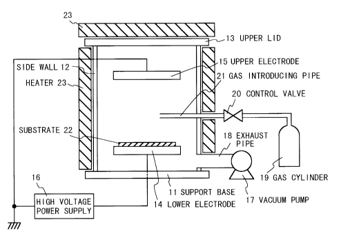
Fig. 2 is a cross sectional view which shows the
structure of a plasma enhanced chemical vapor deposition
apparatus according to the first embodiment of the present
invention. This chemical vapor-phase growth equipment is
used to form an amorphous carbon thin film on a substrate 22.
Referring to Fig. 1, in the chemical vapor deposition
apparatus, a reaction chamber is composed of a support base
11, a cylindrical side wall 12 which is arranged on the
support base 11, and an upper lid 13 provided to oppose to
the support base 11 and to close the other end of the
cylindrical side wall 12. An exhaust pipe 18 is attached to
the side wall 12 to be connected to a vacuum pump 17. A gas
introducing pipe 21 for introducing a material gas into the
reaction chamber penetrates the side wall 12. The gas
introducing pipe 21 has an opening in the reaction chamber at
one end and the other end is connected via a control valve 20
to a gas cylinder 19 as a gas supply source. A lower plate
electrode 14 and an upper plate electrode 15 are arranged in
218520~
- 10 -
parallel to each other and to oppose to each other in the
reaction chamber. A substrate 22 for the amorphous carbon
film to be formed is mounted on the lower electrode 14. The
upper electrode 15 is grounded and a predetermined voltage is
applied to the lower electrode 14 by a high voltage power
supply 16. The reaction chamber further includes a heater 23
is added around the side wall 12 and on the upper lid 13 such
that the heater 23 covers the outside of the reaction
chamber, i.e., covers these side walls 12 and the upper lid
13. The heater 23 is used to heat the wall of a reaction
chamber, especially the inner surface of a side wall 12 and
an upper lid 13 where deposition of adhesion becomes the
problem, to a predetermined temperature, for example, a
temperature equal to or higher than 200 C.
Next, the film formation of the amorphous carbon thin
film using this chemical vapor-phase growth equipment will be
described. As a material gas, a hydrocarbon gas of CH4 is
used for example. When a film containing fluorine is to be
deposited, a carbon fluoride gas of CF4 and so on is used as
the material gas~ The hydrocarbon gas and carbon fluoride
gas may be properly mixed. If the amorphous carbon thin film
which contains nitrogen or silicon is to be formed, a N2 gas
or a silane group gas such as SiH4 and Si2H6 and so on should
be added to these material gases. Then, the inside of the
reaction chamber is decompressed by the vacuum pump 18 via
the exhaust pipe 18. The material gas is introduced from the
gas cylinder 19 into the reaction chamber via the control
218520~
- 11
valve 20. The inner wall of the reaction chamber is heated
to a temperature equal to or higher than 200 C by the heater
23. High frequency electric power is applied between a lower
electrode 14 and an upper electrode 15 by the high voltage
power supply 16 so that plasma discharge is generated.
Thereby, an amorphous carbon thin film is formed on the
substrate 22 mounted on lower electrode 14 while preventing
any adhesion from depositing on the inner wall of the
reaction chamber. In this case, because any adhesion is not
deposited on the inner wall of the reaction chamber and
active particles generated by the plasma discharge can be
effectively used for the deposition on the substrate 22, the
thin film such as the amorphous carbon thin film can be grown
with good quality and high growth rate. In this example, the
high frequency discharge is used as a plasma generating
source. However, as the plasma generating source, direct
current discharge, microwave discharge, helicon wave
discharge can be also used. The present invention can be
applied to the case to use these plasma sources.
Next, the reason for setting the temperature of the
inner wall of the reaction chamber to a temperature equal to
or higher than 200 C will be explained. Figs. 3 and 4 show
the measuring results of the temperature dependency of the
film deposition rate to the side wall of the reaction chamber
when the methane (CH4) is used as the material gas and an
amorphous carbon thin film is formed by the parallel plate
type plasma chemical vapor deposition apparatus. Fig. 3
2185203
- 12 -
shows the experimental results when the electric power
(source electric power) for the plasma generation is fixed on
200 W and the internal pressure of the reaction chamber is
0.1, 0.2, 0.3 Torr, respectively. Fig. 4 shows the
experimental results when the internal pressure of the
reaction chamber is fixed on 0.1 Torr and the source electric
power is set to 100, 200, 300 W, respectively. From these
experiment results, it is found that the deposition rate
decreases as the temperature of the side wall increases and
the adhesion probability of the thin film (adhesion) to the
side wall becomes 0 when the temperature of the side wall
reaches 200 C.
This shows that the adhesion probability to the
substrate and so on of the film formation active particles
which are activated by the plasma has great temperature
dependency and the adhesion probability to the inner wall of
the reaction chamber is made to be substantially 0 at about
200 C. Also, as shown in Figs. 3 and 4, the temperature
that the adhesion to the side wall becomes 0 is constant at
200 C without undergoing the influence of the high frequency
electric power (the source electric power) or the pressure.
From these results, it could be considered that even if the
source electric power and pressure are changed so that the
kind and density and so on of the active particles in the
plasma are changed, the adhesion coefficient of any of those
active particles would become 0 at 200 C. Therefore, if the
inner wall of the reaction chamber is heated to a temperature
~185203
- 13 -
equal to or higher than 200 C, no deposition of the adhesion
to the inner wall would be generated. Actually, when the
whole inner wall of the reaction chamber was heated to 200 C
and an amorphous carbon thin film was formed, deposition of
adhesion to the inner wall of the reaction chamber could be
prevented.
When a gas other than the methane gas is used as the
material gas, the temperature dependency of adhesion to the
inner wall was established in the same manner as mentioned
above. That is, in either case of using a hydrocarbon gas
such as C2H6, C2H4, C2H2, or C6H6 and a carbon fluoride gas such
as CF4, C2F6, or GF6 as the material gas, the adhesion
probability of a film to the inner wall became 0 when the
wall temperature became 200 C. Also, when the whole wall of
the reaction chamber was heated to 200 C and an amorphous
carbon thin film was formed using these material gases,
adhesion to the inner wall of the reaction chamber could be
prevented. The same result was obtained in a case where a N2
gas, or a SiH4 gas, a Si2H6 gas were added to the material gas
and an amorphous carbon thin film which contained nitrogen or
silicon was formed. Further, in the plasma chemical vapor
deposition apparatus using direct current discharge,
microwave discharge, helicon wave discharge, when the
reaction chamber was heated to 200 C in the same manner as
described above, the adhesion of a film to the inner wall of
the reaction chamber could be prevented.
Next, the material which constitutes the reaction
2185203
chamber will be described. When the reaction chamber of the
chemical vapor deposition apparatus shown in Fig. 2 is made
of stainless steel, because a thermal conductivity of
stainless steel is small and heat conduction from the heater
23 is different in place, so that a part of the inner wall of
the reaction chamber cannot be raised to 200 C, the
deposition of adhesion one is seen only about the part. For
this reason, in a case where the reaction chamber made from
stainless steel, the heating temperature of the reaction
chamber is set to 250 C such that the whole inner wall of
the reaction chamber is heated to a temperature equal to or
higher than 200 C, even if a temperature decreased part is
formed on the inner wall of the reaction chamber due to the
change of thermal conduction in place. As a result, the film
deposition to the inner wall of the reaction chamber can be
totally suppressed.
On the other hand, the reaction chamber is made from
aluminum which has a great thermal conductivity and is heated
to 200 C by the heater 23. As a result, the whole reaction
chamber is uniformly heated to 200 C. In this state, an
amorphous carbon thin film is formed. As a result, the film
deposition to the inner wall of the reaction chamber is not
seen. In this manner, if the reaction chamber is made from
metal with a great thermal conductivity, the deposition of
adhesion to the inner wall of the reaction chamber can be
totally prevented at a temperature lower than in a case where
the reaction chamber is made from stainless steel.
- 2185203
- 15 -
Fig. 5 is a cross sectional view which shows the
structure of the plasma chemical vapor deposition apparatus
according to the second embodiment of the present invention.
This chemical vapor deposition apparatus is used to form an
amorphous carbon thin film on a substrate 22. In the
parallel plate type plasma chemical vapor deposition
apparatus according to the second embodiment, the heater 23
is removed from the plasma chemical vapor deposition
apparatus shown in Fig. 2. Instead, the reaction chamber is
made from electrically conductive metal such as stainless
steel and aluminum in the second embodiment. Further, the
plasma chemical vapor deposition apparatus according to the
second embodiment is constituted in such a manner that a bias
voltage can be applied to the reaction chamber by a high
voltage power supply 24. The bias voltage is DC voltage or
high frequency voltage. Further, in addition to the high
voltage power supply 24, there is provided a shield member 25
which is constituted of metallic network and so on to
surround the whole reaction chamber and is grounded.
Next, the formation of an amorphous carbon thin film
using the chemical vapor deposition apparatus will be
described. As a material gas, is used a hydrocarbon gas such
as CH4 and so on or a carbon fluoride gas such as CF4 and so
when the film containing fluorine is to be formed. The
hydrocarbon gas and the carbon fluoride may be properly
mixed. If the amorphous carbon thin film which contains
nitrogen or silicon is to be formed, a N2 gas or a silane
2185203
- 16 -
group gas such as SiH4 and Si2H6 and so on should be added to
these material gases. Then, the inside of the reaction
chamber is decompressed by the vacuum pump 17 via the exhaust
pipe 18. The material gas is introduced from the gas
cylinder 19 into the reaction chamber via the control valve
20. High frequency electric power is applied between the
lower electrode 14 and the upper electrode 15 by the high
voltage power supply 16 such that plasma discharge occurs.
Further, a bias voltage of direct current or high frequency
is applied to the whole reaction chamber by the high voltage
power supply 24, so that the amorphous carbon thin film is
formed on the substrate 22 mounted on the lower electrode 14
without depositing any adhesion to the inner wall of the
reaction chamber. In this example, the high frequency
electric power is applied between the lower electrode 14 and
the upper electrode 15 such that the plasma is generated in
the reaction chamber. However, it is possible to use direct
current discharge, microwave discharge, helicon wave
discharge as a plasma generation source. The present
invention can be also applied to cases using these plasma
sources.
Next, the bias voltage applied to the reaction
chamber will be described. Fig. 6 shows the adhesion rate of
the amorphous carbon film to the inner wall of the reaction
chamber when dc or ac bias voltage is applied to the reaction
chamber using the above-mentioned chemical vapor deposition
apparatus. Thus, in a case where the amorphous carbon thin
2185203
film is formed using a hydrocarbon gas such as C2H6, C2H4,
C2H2, or C6H6 or a carbon fluoride gas such as CF4, C2F6, or
C4F8 as the material gas, it is found that the adhesion of
the film to the inner wall of the reaction chamber can be
prevented when the dc electric power or the high frequency
electric power outputted from the high voltage power supply
24 is controlled such that the bias voltage equal to or less
than -100 V can be applied to the reaction chamber. That is,
by applying the dc or high frequency bias electric power is
to the inner wall of the reaction chamber in a case of
formation of the film, ion particles which is generated by
the plasma are accelerated and irradiated to the inner wall
of the reaction chamber so that etching and sputtering to the
film which is adhered to the inner wall would be performed,
resulting in prevention of adhesion of the film to the inner
wall. In this case, as illustrated in the figure, even if
the plasma is generated using any source electric power, the
deposition to the inner wall of the reaction chamber can be
suppressed if the bias voltage equal to or less than -100 V
is applied to the reaction chamber. That is, ions
accelerated by the bias voltage equal to or less than -100 V
(being equal to or more higher 100 V at the absolute value)
to have a high energy contribute to the reduction of the
adhesion coefficient to "0". It is shown for the ions to be
generated in the same method even if any source electric
power is used.
In a case of using any plasma source which uses a
2185203
- 18 -
plasma source of a direct current discharge type, microwave
type, helicon wave type other than the parallel plate type,
the adhesion of the film to the inner wall of the reaction
chamber could be prevented in the same manner as described
above by applying the bias voltage equal to or less than -100
V to the reaction chamber. The same result could be obtained
in a case where a N2 gas, or a gas of SiH4 and Si~H6 were
added to the material gas to from the amorphous carbon thin
film which contains nitrogen or silicon.
According to the present embodiment, the particle
generation can be prevented without cleaning the inside of
the reaction chamber every predetermined constant time
period. Also, although a part of the active particles is
conventionally deposited on the side wall, because all the
active particles are deposited only on the substrate, the
film formation rate on the substrate can be increased about
twice.
As described above, in the present invention, when an
amorphous carbon thin film is formed using the plasma
enhanced chemical vapor deposition method, the reaction
product can be prevented from adhering to the inner wall of
the reaction chamber by heating the reaction chamber to a
temperature or above at which the adhesion coefficient of the
film formation active particle to the inner wall of the
reaction chamber becomes 0, or by applying the direct current
or high frequency bias voltage to the reaction chamber. In
this manner, there is achieved the advantage that it is not
218~203
- 19 -
necessary to perform regular removal of the adhesion from the
reaction chamber , i.e., the effect to make maintenance free.