Note: Descriptions are shown in the official language in which they were submitted.
- 2~3~4
Title: DIGITAL DATA CROSSPOINT SWITCH
WITH MIRROR PIN-OUTS
FIELD OF THE INVENTION
This invention relates to a mirror pin-out arrangement for a
5 digital data crosspoint switch.
BACKGROUND OF THE INVENTION
Crosspoint switches are electronic devices that are used to
route inputs to outputs using a programmed configuration. The input/
output mapping can be altered at any time utilizing programming inputs
10 to the device, so that a configurable switching matrix can be designed.
One of the challenges in digital data switching matrix design
is to connect multiple crosspoint devices together to create larger switching
matrices. In the past this has required the use of complex multi-layer
circuit boards and high speed switches/multiplexers to multiplex inputs to
15 multiple crosspoint devices.
Improvements in such crosspoint devices are described in the
copending application of Eric Fankhauser and assigned to the assignee of
the present invention, and filed concurrently herewith. (A copy of the
disclosure and drawings of that application is attached as Appendix A
20 hereto and is incorporated by reference herein.) However there remains a
need for additional simplification.
BRIEF SUMMARY OF THE INVENTION
Accordingly, it is an object of the invention to provide a pair
of crosspoint devices each having the same electrical characteristics, but in
25 which the pin-outs have been mirrored across the vertical axis of one
device as compared with the other. This allows simplified connection of
the devices in matrices as will be explained.
In one aspect the invention provides a set of first and second
crosspoint devices, each containing a crosspoint switch and each having
218~30~
- 3 -
first and second opposed sides and third and fourth opposed sides, and
wherein in said first device, said first side contains input pins, said second
side contains control pins, said third side contains expansion data input
pins, and said fourth side contains output pins, and in said second device,
5 said first side contains control pins, said second side contains input pins,
said third side contains expansion data input pins arranged in the reverse
order from that of the expansion data input pins of said first side of said
first device, and said fourth side contains output pins arranged in the
reverse order from that of the output pins of said first device.
Further objects and advantages of the invention will appear
from the following description, taken together with the accompanying
drawings.
BRIEF DESCRIPTION OF THE DRAWINGS
In the drawings: -
Fig. 1 is a plan view of a set of devices according to the
invention and showing the mirror pin-out configuration;
Fig. 2 is a block diagram showing a 16 x 16 matrix using two
sets of two devices each according to the invention;
Fig. 3 is a side view of a printed circuit board containing the
- 20 devices of Fig. 2;
Fig. 4 is a block diagram showing two sets of two devices each
according to the invention arranged in a 32 x 8 matrix; and
Fig. 5 is a side view of a circuit board containing the devices of
Fig.4.
DETAILED DESCRIPTION OF PREFERRED EMBODIMENTS
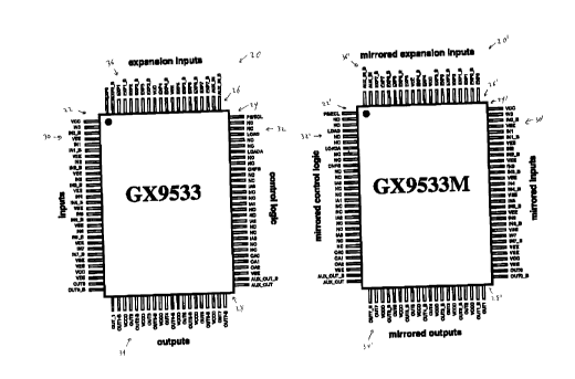
Reference is first made to Fig. 1, which shows a device 20
having left and right sides 22, 24, and top and bottom sides 26, 28. Input
pins 30 are connected to side 22, including eight sets of input data pins
marked from IN0, IN0-B to IN7, IN7-B.
The right hand side 24 of the device 20 contains control pins
3 0 4
- 4 -
32. The bottom side of the device 20 contains output pins 34, while the top
side of the device contains expansion data input pins 36, for additional
data inputs (as described in connection with said copending application).
Also shown in Fig. 1 is device 20, which is the mirror image
5 of device 20 about the vertical axis of device 20. In device 20, pin-outs and
reference numerals have been marked with the prime symbol to
distinguish them from those of device 20.
In device 20', it will be seen that the input pins 30 are now on
the right hand side 24'of the device as drawn, while the control input pins
10 32' are on the left hand side 22' of the device. The expansion data input
pins 36 remain at the top side 26 of the device but have been reversed in
order as compared with device 20. Similarly the output pins 34' remain at
the bottom side 28' of the device 20 but have again been reversed in order.
The arrangement shown in Fig. 1 allows switching matrix
15 designers to deploy the two versions shown (the standard pin-out version
20 and the mirror pin-out version 20') on each side of a circuit board 40, as
shown in Figs. 2, 3. Fig. 2 displays sides A and B of the circuit board 40, so
that when the two halves of Fig. 2 are folded about vertical line 42, the
complete circuit board 40 will be obtained (as shown in Fig. 3). Side A
20 contains two devices 20 while side B contains two devices 20'.
As shown for side A of Fig. 2, the data inputs 46, 48 are
received from the left hand side of the devices 20 and enter the devices 20
directly. In addition the traces which provide the inputs 46, 48 extend
through vias in the circuit board 40 to the mirror devices 20 and serve as
25 inputs to them as well. The remaining data pins of the devices 20, 20' are
not connected together and therefore no additional vias are needed for
them in the circuit board 40.
It will be seen that the arrangement in Figs. 2 and 3 permits
an extremely compact 16 x 16 matrix using four devices (two standard
30 devices and two mirror devices) connected together.
If additional vias in the circuit board are permitted to feed the
output signal back and forth between the two sides of the circuit board,
218~30~
then the arrangement shown in Figs. 4 and 5 may be used. Again Fig. 4
shows sides A and B of a circuit board 50, it being assumed that the two
sides will be folded about vertical line 52 to produce the final circuit board,
which is shown in Fig. 5.
In Fig. 4, the inputs for standard devices 20-1, 20-2 come from
the left hand side of the devices. These are inputs 0 to 7 and 16 to 23. On
side B, the inputs 8 to 15 and 24 to 31 are received from the right hand side
of the mirror devices 20 -1, 20-2. This produces a 32 x 8 design, using four
8 x 8 devices.
As shown in Fig. 5, the output from device 20-1 travels
through traces 60 beneath device 20-1 (on the circuit board 50) and then
through vias 62 of circuit board 50 to the expansion data inputs 36'-1 of
mirror device 20'-1. The outputs of mirror device 20'-1 travel through
traces 64 beneath device 20'-1, through vias 66 on the circuit board to the
expansion data inputs 36-2 of standard device 20-2.
The outputs 34-2 of standard device 20-2 again travel on traces
68 beneath device 20-2, through vias 70 in the circuit board 50 to the
expansion data inputs 36-2 of mirror device 20-2. The outputs 34'-2
(outputs 0 to 7) of mirror device 20-2 constitute the eight outputs of the
matrix.
An advantage of the arrangement shown is that it permits an
extremely compact design while minimizing the need for vias, complex
printed circuit boards, and while reducing the resultant crosstalk which
can occur in the circuit board.
While preferred embodiments of the invention have been
described, it will be appreciated that various changes may be made within
the spirit of the invention and all such changes are intended to be
included in the scope of the accompanying claims.
CA2 1 '~530~1f
._ .
APPENDIX A
Title: CROSSPOINT SWITCH WITH IMPROVED PIN-OUTS AND
EXPANSION INPUTS
FIELD OF THE INVENTION
This invention relates to a crosspoint switch. In particular it
relates to a unique pin-out arrangement for a crosspoint switch, and to
expansion input port architecture for a crosspoint switch.
BACKGROUND OF THE INVENTION
Crosspoint switches are electronic devices that are used to
route data inputs to data outputs via a programmed configuration. The
input/ output mapping can be altered at any time using programming
logic inputs to the device, so that a configurable switching matrix can be
designed.
One of the significant challenges in digital data sw-itching
matrix design is the connection of multiple crosspoint switches or devices
together to create larger switching matrices. In the past this has been
accomplished by using complex multilayer circuit boards, and high speed
switches or multiplexers which are connected to multiple crosspoint
devices.
The use of external multiplexers and complex printed circuit
boards has led to many difficulties, including difficulties in assembling the
matrix into a compact configuration, crosstalk problems, and difficulty in
terminating traces on the circuit board.
BRIEF SUMMARY OF THE INVENTION
Accordingly, it is an object of the present invention in one of
its aspects to provide a pin-out arrangement for a digital data crosspoint
switch which facilitates the design of a switching matrix using a number of
individual crosspoint devices, and which at the same time reduces signal
crosstalk and circuit board routing complexity. In this aspect the invention
1 Y~'fl 2 ' 8530l,l
provides a crosspoint device containing a crosspoint switch and having:
(a) first and second opposed sides,
(b) a plurality of input pins on said first side,
(c) a plurality of second pins on said second side, a second
pin being located opposite at least some of said input
pins,
(d) some of said input pins being data input pins coupled
to said crosspoint switch,
(e) the second pins opposite said data input pins being "no
connect" pins which are not electronically connected to
said crosspoint switch.
In another aspect the invention provides expansion input
ports for digital crosspoint devices, so that the devices can again be
assembled in a matrix in a simple manner while reducing the need for
complex printed circuit boards and also reducing input/output crosstalk.
In this aspect the invention provides a crosspoint device containing a
crosspoint switch and having:
(a) first and second opposed sides,
(b) a plurality of input pins on said first side,
(c) a plurality of second pins on said second side,
(d) some of said input pins being data input pins coupled
to said crosspoint switch,
(e) said device also having a third and a fourth side each
extending between said first and second sides, said
third side containing output pins and said fourth side
containing expansion data input pins coupled to said
output pins,
(f) said expansion data input pins being self terminated.
Further objects and aspects of the invention will appear from
30 the following description, taken together with the accompanying
drawings.
8 rA2~. ~530~
BRIEF DESCRIPTION OF THE DRAWINGS
In the drawings:
Fig. lA is a block diagram of a prior art multiplexed input
array of crosspoint devices;
Fig. lB is a block diagram of another prior art input array of
crosspoint devices;
Fig. 2 is a block diagram of a multiplexed output array for
crosspoint devices;
Fig. 3 is a block diagram showing prior art bussed outputs for
a crosspoint device array;
Fig. 4A is a diagrammatic view of a pair of crosspoint devices
according to the invention;
Fig. 4B is a diagrammatic view of a portion of a printed circuit
board showing traces used with the device of Fig. 4A;
Fig. 5 is a block diagram of a crosspoint device having
expansion input port architecture;
Fig. 6 shows in more detail a portion of the Fig. 5
arrangement;
Fig. 7 is a block diagram showing a matrix of devices
connected together and using the expansion input port architecture of Figs.
5 and 6; and
Fig. 8 shows optional detail for the Figs. 5 and 6 device.
DETAILED DESCRIPTION OF PREFERRED EMBODIMENTS
Reference is first made to Fig. 1, which shows a conventional
prior art crosspoint switch array having two n x n crosspoint devices 20, 22
having inputs 24, 26. In the past it was common to connect multiple
crosspoint devices together to create larger switching matrices by the use of
complex multi-layer circuit boards and high speed switches or
multiplexers, such as multiplexer 28. Multiplexer 28 is connected to the
inputs 24, 26 to create an n x m switching matrix, where n<m. Similarly,
the outputs of the crosspoint devices were required to be multiplexed
together to create a switching matrix, as shown in Fig. 2. In Fig. 2 the
C~'i21 8530a
outputs 30, 32 of crosspoint devices 20, 22 are connected to another
multiplexer 34 having outputs 36. (Alternatively, the inputs of crosspoint
devices 22, 24 can simply be connected together as shown in Fig. lB, but
this is not suitable for their outputs, as will be discussed.)
5It is possible to provide devices which have outputs which
are turned "on" or "off" utilizing a configuration interface. These
switching matrix designs would not require external multiplexers in order
to be connected together, and are illustrated in Fig. 3, where two switching
crosspoint devices 40, 42 are illustrated as being connected together at
10connections 44 on a circuit board 46. Unfortunately, the design shown in
Fig. 3 may suffer from crosstalk problems, particularly in the connection
area 44 where the output traces 48 of one crosspoint device 40 cross the
output traces 50 of the other crosspoint device 42. In addition, it will suffer
from signal degradation from the interconnection of "off" outputs with
15"on" outputs. Further, since vias in the circuit board are required to
connect the crosspoint devices' outputs to the output bus, additional
crosstalk problems can occur. The output traces on the circuit board are
also difficult to control and to terminate properly.
Reference is next made to Fig. 4A, which shows a crosspoint
20device 54 which facilitates connection of the device to a printed circuit
board, and which also has other advantages which will be described.
The crosspoint device 54 of Fig. 4A is rectangular in plan,
having left and right sides 56, 58 and top and bottom sides 60, 62. The
device 54 has input pins 64 at its left hand side, output pins 66 at its bottom
25side, control pins 68 at its right hand side, and self terminated expansion
input pins 70 (to be described) at its top side. All of these pins, whether
used or not, are soldered to the circuit board 72 (Fig. 4B) to which the
device 54 is connected, for a secure mechanical connection.
It will be seen that the input pins 64 include a number of data
30input pins marked from IN0, IN0-B to IN7, IN7-B. According to the
invention, the pins on the side of the device 54 opposite to these input
data pins, namely pins 74, are "no connect" pins and are not used for any
other purpose. As best shown in Fig. 4B, the circuit board traces 76 which
'' '' iu C421~530a
carry the data inputs to the data input pins IN0, IN0-B to IN7, IN7-B are
bussed across the circuit board and are connected to the "no connect" pins
74 and continue across the circuit board to be connected to the next
crosspoint device 54A, as shown in Fig. 4A.
Because the only pins on the right hand side 58 of the device
54 which are connected to the circuit board traces 76 are the "no connect"
pins 74, and since pins 74 are not connected to any internal circuitry in
device 54, it is possible to route the circuit board traces 76 along a single
layer of the circuit board 72. There is no need to have these traces routed
down to a lower layer of the circuit board to go under the pins 74 and then
to route them back up to the surface of the board for connections.
The arrangement shown in Figs. 4A and 4B therefore has a
number of advantages. Firstly, it lowers the complexity of the circuit board
72 needed to hold a matrix of crosspoint devices, since fewer layers are
needed for the circuit board. Secondly, it reduces the signal degradation
effects which would normally be caused by vias and corners in the printed
circuit board traces for high frequency digital data such as serial digital
video data. Thirdly, it facilitates the simple design of large matrices made
from individual crosspoint devices, and it allows higher crosspoint device
density on a switching matrix circuit board. Finally, it allows all inputs to
have a single line termination, since any number of devices can be located
on a single trace 76, and yet only one termination is needed, at the end of
that trace.
Reference is next made to Fig. 5, which shows expansion
input port architecture for a crosspoint device 54. In the past, crosspoint
devices have normally included data inputs 80 (connected to the data
input pins of Fig. 4A), directed to an input buffer 82, which in turn is
connected to the matrix (shown for example as an 8 x 8 matrix) 84 of
crosspoints or switches. The matrix 84 is in turn connected to the matrix
an output buffer 86 connected to data outputs 88 (the output pins OUT1,
OUT1-B to OUT7, OUT7-B of Fig. 4A). The control inputs 90 are in turn
connected to control input latches 92 which are used to control the matrix
84.
ll CA 21 ~ 5304
A difficulty with the prior art arrangement as described is that
it has been very difficult to connect multiple crosspoint devices together in
a matrix. Since external multiplexers were used, the architecture became
cumbersome.
As shown in Fig. 5, the invention in one aspect provides self
terminated expansion data inputs 96 on the top side 60 of the crosspoint
device 54. These are connected to pins EXP0, EXP0-B to EXP7, EXP7-B of
Fig. 4A. The reference to "self terminated" means that there is a
transmission line impedance 97 (Fig. 6) located internal to the expansion
port input. An impedance 97 is thus connected across each pair of pins
EXP0, EXP0-B to EXP7, EXP7-B. This impedance can take the form of an
active device (Bipolar, MOS, FET transistor(s)) or circuit or a passive device
(resistor, capacitor, inductor) or circuit. Resistors 97 are shown as an
exemplary implementation. Resistors 97 are integrated as part of the
device 54 and are not external. The self terminated expansion data inputs
96 are connected through buffer 98 to a 2 x 1 multiplexer 100, which is in
turn connected to the crosspoint matrix 84 and to the data output buffer 86.
In Fig. 5 the control inputs 90 control the crosspoint matrix 84 as usual and
also control the multiplexer 100 so that the desired outputs (either from
the data inputs 80 or directly from the self terminated expansion data
inputs 96, as selected) are fed to the combined output stage and buffer 86
and hence to the data outputs 88.
It will be seen that in operation, the multiplexer 100, under
control of the control latches 92, will direct either the outputs from the
crosspoint array, or the expansion data inputs, to output buffer 86, and
hence to the data outputs 88. Thus, data received on the self terminated
expansion data inputs is routed directly through the device 54 to the data
outputs, rather than being routed through the circuit board. This allows
additional devices to be added easily to widen the matrix, as explained in
connection with Fig. 7.
Fig. 7 shows an example in which four crosspoint devices 54-
1, 54-2, 54-3, 54-4 are connected together in a matrix. As shown, the data
inputs 80-1 for device 54-1 are connected to the input pins 64-1 of device
54-1 and are also bussed across device 54-1 and are connected to the input
1~ rJ~21 85304
pins 64-2 of device 54-2 (using the arrangement of Figs. 4A, 4B).
A second set of data inputs 80-2 is connected to the data input
pins 64-3 of device 54-3 and is also bussed across device 54-3 and connected
to the data input pins 64-4 of device 54-4, again using the arrangement of
Figs. 4A, 4B.
The data outputs 88-1 of device 54-1 are connected to the self
terminated expansion data inputs 96-3 of device 54-3. Similarly, the data
outputs 88-2 of device 54-2 are connected to the self terminated expansion
data inputs 96-4 of device 54-4. The data outputs of devices 54-3, 54-4 are
shown at 80-3, 80-4 respectively.
The arrangement shown in Fig. 7 avoids the need to run
traces from the outputs of the crosspoint device to a common output bus,
and therefore crosstalk between output channels, and signal degradation
due to signal reflections on the transmission line, can be greatly reduced.
In addition, in the Fig. 7 arrangement fewer circuit board layers are needed
since the data outputs of each device simply line up. Further, because the
data outputs are routed from the top of the switching matrix to the bottom
through the devices 54 themselves and not beneath the devices, inputs can
be simply bussed across the board without concern about input/output
crosstalk (since the data input traces 76 do not cross output traces in the
circuit board). The use of self terminating expansion ports eliminates the
need for external line terminating resistors, allowing a much denser
interconnect between the data outputs of one crosspoint device and the
expansion port inputs of another crosspoint device.
Reference is next made to Fig. 8, which shows a power saving
arrangement. Normally each crosspoint device 54 has an output voltage
of approximately 800 mv. However the devices 54 themselves can be
made to operate with data input voltages of only 400 mv. Therefore each
device 54 has the ability to provide data outputs at 400 mv when it is
driving the expansion input part of another device 54, or to provide data
outputs at 800 mv when it is driving an external device such as an ECL
logic gate or other electronic component which requires ECL or pseudo
ECL type input logic levels in the range of an 800 mv signal swing.
1 3 C A 2 1 ~ 5 3 0 d
In addition to reducing the output voltage by one half, the
associated internal current required to bias the output stage can also be
reduced by one half for the same load impedance (i.e. 100 ohms), or by
more than half if the load impedance is increased (e.g. to 200 ohms).
For this purpose, and as shown in Fig. 8, each output stage
and buffer 86 is controlled by bandgap reference control circuit 100, which
in turn is controlled by an external resistor 102. Depending on the value of
resistor 102, the control circuit 100 sets the data outputs 88 at 400 mv or 800
mv .
Typically there are three modes of operation, as follows:
Output
Value of OutputStage Diffele,ltial
Mode Resistor 102 ECL Voltage Load Drive Power
2 KQ 800 mv 100 Q normal
2 4 KQ 400 mv 100 Q lower
3 6 KQ 400 mv 200 Q lowest
The load drive resistors of 100 ohms (not shown) will simply
be external resistors connected across the differential data outputs. The 200
ohm resistors are the integrated resistors 97.
Using the Fig. 8 arrangement, the devices 54-1, 54-2 in Fig. 7
15 can for example be operated at lowest power, since they are simply driving
further devices 54-3, 54-4. The devices 54-3, 54-4, whose outputs are
connected to external circuits, will be operated at normal power. This
arrangement saves power and reduces heat dissipation.
While preferred embodiments of the invention have been
20 described, it will be appreciated that various changes can be made within
the spirit of the invention, and all are intended to be within the scope of
the appended claims.