Note: Descriptions are shown in the official language in which they were submitted.
WO 95/28073 2 1 8 5 ~ 8 7 PCTISE9~/00359
An aL~ lL for shi~l(lin~ and/or cool~ng electronic
~ Ls ~unted on a circuit board.
TEC~NICAL FII~LD
The present invention relates to a arrangement for shielding
and/or cooling electronic components mounted on a circuit
board. The arrangement includes a generally planar shielding
hood having downwardly extending side edges extending around
the perimeter thereof and intended for enclosing the com-
ponents, and a cooling element having a generally planar
underside and cooling fins or flanges arranged on its upper
side.
D158CRIPTION OF Tms R~ qRWND ART
Present day IC-components are becoming more and more in-
tegrated and therewith more complex. Furthermore, clock
frequencies and power generation constantly increase.
Microprocessors are a typical case. Parameters such as heat
generation and disturbance sensitivity increase with the
increasing complexity of IC-components, neC~csitating the
need to shield and cool said components. At present, there is
no effective economic or technical solution which combines
these requirements, which in reality contradict one another.
The importance of providing effective screening or shielding
of IC-components is reflected among other things in the
discussions in present day mass media concerning, for instan-
ce, how mobile telephones render diserviceable the electro-
nics of motor vehicles, such as cars. There is therefore apronounced need of a technically simple and economic shiel-
ding/cooling construction which will fullfil simultanoeusly
the stringent requirements placed on both these facilities.
WO 95/28073 PCT/SE95/00359
2~ 85q87 2
DI8CI,08URI~ OF T~EB INV~ ION
The object of the present invention is to solve the aforesaid
problem at low costs, by providing an arrangement which can be
used either to solely shield an electronic component or solely
cool an electronic component or which can be used to both
shield and cool an electronic component in a simple manner and
at low cost. This object is achieved by means of an arran-
gement having the characteristic features set forth in the
following claims.
The inventive arrangement functions on the principle that in
addition to functioning as a shield, the shielding hood shall
also conduct heat to a cooling element. The construction is
extremely flexible, and enables the following combinations to
be obtained with precisely the same elements: shielding and
cooling, solely shielding or solely cooling.
When nee~ing to both cool and shield an electronic component,
the shielding hood is used as a cooling means and as a heat
conducting means and is placed betwen the heat source, for
instance an IC-circuit, and a cooling element. In order not to
obtain an eYceceively large thermal transition resistance,
the shielding hood and cooling element must have well-defined
abutment surfaces with the heat source. This is achieved by
configuring both the shielding hood and the cooling element in
a manner appropriate to the purpose inten~e~.
The primary characteristic feature of the invention resides
in the ability to combine cooling and shielding.
An embodiment of the invention at present preferred includes
significant characteristic features which will now be
described in more detail with reference to the accompanyin~
drawings.
W095/28073 2 1 8 5 ~ 8 7 PCT/SE95/00359
BRI~F D~8CRIP~ION OF TB DRA~ING8
- Figure 1 is a perspective view of the elements included in the
inventive arrangement.
Figure 2 is a sectional view showing the arrangement
mounted over a component.
Figures 3 and 4 are respective perspective views of the
arrangement when used solely for shielding and solely for
cooling respectively.
Figure 5 is an alternative embodiment of an arrangement
which is effective for both shielding and cooling purposes.
BE8T MODB OF CARRYING O~T T~E INVENTION
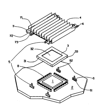
Figure 1 illustrates in perspective those elements which are
included in an inventive arrangement. The illustrated
arrangement is intended for shielding and/or cooling a
component 1, for instance an IC-component, mounted on a
circuit board 2. The arrangement includes a generally planar
shielding hood 3, a generally planar cooling element 4,
fastener means 5 in the form of hook means 6 and holder means
7 respectively, and contact springs 8.
The shielding hood 3 has downwardly exten~ing side edges 31
and the size of the hood is adapted to the size of the com-
ponent 1, so that the component will be fully surrounded by
the side edges. The hood 3 is secured to the board 2, by
- pressing the side edges 31 into contact springs 8 which are
surface mounted on the board around the component 1. The side
edges include nibs 33 which function to lock the hood firmly
in the contact springs. The hood 3 is intended primarily for
shielding the component, although it shall also be capable of
functioning as a means for conducting heat to the cooling
W095/28073 PCT/SE95/00359
21 859a7
element 4 when the arrangement is also intended for cooling
purposes. To this end, it is necessary for the surface of the
hood 3 that abuts the component to be well defined, so that
the thermal transition resistance will not be too large.
Accordingly, the hood has the form of a relatively rigid frame
having a thinner central part 32 which is joined to the frame
and which can move in relation thereto. The thinner part 32
functions as a movable diaphragm which is pressed against the
component 1 with the aid of the cooling element 4. This
mobility of the diaphragm enables the height of the hood or
cover in relation to the height of the component to be readily
adapted so as to ensure that positive abutment is achieved
with a small heat transition resistance between component and
cooling element, as shown in the sectioned view of Figure 2.
The heat emitting surface area of the cooling element 4 is
enhanced with the aid of a plurality of cooling fins 41
disposed on the upper side of the element. In addition, the
cooling element 4 has a well defined abutment surface cor-
responding to the shielding hood 3, so as to reduce the
resistance to thermal transition or transfer. As shown in the
sectioned view of Figure 2, the underside of the cooling
element4 has a downwardlydirected, flat outwardlyprojecting
part 42 which may either lie against the central part, the
diaphragm 32, of the hood 3 when both shielding and cooling
are required, or directly against the component 1 when only
cooling is required.
The cooling element 4 is held in place on the circuit board 2
with the aid of anchoring means 5 which in addition to
providing a force which presses the cooling element, and the
central part 32 of the hood, against the component also
connects the cooling element 4 electrically to earth. In this
regard, it is important that the cooling element is connected
to earth at each corner. The anchoring means 5 are comprised
of hook means 6 mounted on the surface of the board 2, and
W095l28073 2 1 8 5 q 8 7 PCT/SE95/00359
holder means 7, mounted on the cooling element 4, which coact
with respective hook means. Each hook means 6 has a generally
U-shaped profile, whose one leg has the form of a solder pad
61, said solder pads being soldered to corresponding solder
pads (not shown) on the board 2. Each other leg of the profile
has the form of a hooked part 62, which is bent so as to be
upst~n~;ng from the circuit board. The holder means 7 is made
of a resilient material having a part 71 configured to enable
said part to be clamped firmly between two cooling fins 41 on
the cooling element, or, alternatively, in a specially
configuredgroove (not shown) provided onthecoolingelement,
and a stepped second part 72 in which an opening 73 is
provided and which can be brought into resilient or spring
engagement with the hooked part 62 of the hook means 6, as
illustrated in Figure 2. A holder means 7 is placed in each
corner of the cooling element, and a hook means 6 is placed in
a corresponding position on the board 2. The spring effect
thus obtained causes the cooling element 4 to be pressed into
positive abutment with the shielding hood 3 and the component
1 respectively, which, as before mentioned, ensures good
thermal contact between component and cooling element. The
cooling element is, at the same time, positively earthed
through the holding means 7 and the hook means 6, since
anchoring means 5 are placed in each corner.
The above described arrangement is used when a component or
components is/are to be shielded and cooled. When only
shielding is required, only the shielding hood 3 will be used,
as illustrated in Figure 3. The hood is secured in contact
springs 8 placed around the component 1 on the circuit board
2 and disposed so that the side edges 31 on the hood 3 will be
inserted into the springs 8. This provideseffectiveshielding
of the component. The contact springs are also disposed so
that the shielding hood 3 will be secured in the springs with
the aid of the nibs 33, which are arranged on the sides of the
woss/28073 PCT/SE9~/00359
21 85987 6
hood in the manner indicated in Figure 1. The contact spring
8, however, forms no part of the present invention.
When only cooling is required, the proce~re is the same as
that described above although in this case only the cooling
element 4 is used, as illustrated in Figure 4. The cooling
element 4 is secured with the aid of four fastener means 5, in
the same way as that described above.
There is sometimes a need to shield a group of components.
This is made possible by the present invention, in that the
shielding hood 3 is provided in the central part or the
diaphragm 32 with a plurality of openings 34 which form a
defined hole pattern in the hood, as illustrated in Figure 5.
When requiring to cool a component, a cooling element 4 is
placed over the component. The cooling element is affixed with
the aid of four fasteners 5, wherein the hook means 6, and
more specifically the hooked parts 62, extend up through the
opening 34 in the shielding hood 3. In this way, it is
possible to arrange one or more cooling elements 4 with
associated fasteners 5 on the hood 3, above the component or
components 1 that requires/require cooling. However, only one
cooling element has been shown in the Figure for the sake of
clarity.
It will be understood that the aforedescribed and illustrated
embodiment is merely shown by way of example and that various
alternative embodiments are conceivable. For instance the
design of both the cooling element 4 and the fastener 5 and
associated details can be varied in several ways without
departing from the inventive concept.
Consequently, the invention is not restricted to the aforede-
scribed and illustrated embodiments thereof, since modifica-
tions can be made within the scope of the following claims.