Note: Descriptions are shown in the official language in which they were submitted.
218655
TITLE: MONOLITHIC MUI~TILAYER ULTRA THIN CHIP
INDUCTORS AND METHOD FOR MARIN(3 SAME
BACR(~ROUND OF THE INVENTION
FIELD OF THE INVENTION
The present invention relates to monolithic multilayer
chip inductors. More particularly, the present invention
relates to monolithic multilayer chip inductors using
combinations of different coil layers to obtain a desired
number of coil turns.
PROBLEMS IN THE ART
Typical prior art ultra thin inductors consist of two
types. One type requires core assembly by the users, such as
planar inductors where the coil is part of the printed
circuit board. The second type is a planar inductor which is
usually fragile and requires manual placement.
One problem encountered with the prior art chip
inductors is caused by the expansion and contraction of a
circuit board and inductor resulting from a change in
temperature. When the ambient temperature changes, materials
will expand or contract. Different materials expand and
contract at different rates, depending on their coefficient
of expansion. Since the coefficients of expansion of a
circuit board and a chip inductor are different, the circuit
board and chip inductor will expand and contract at different
rates causing mechanical stresses on the ceramic component
and on the circuit board to which it is soldered.
Another problem encountered in the prior art results
from the demand for increasingly small sizes of components.
For example, components to be mounted to a printed circuit
board used in a PCMCIA card must be very thin. Various
problems can result from reducing the size of a component.
For example, as the size decreases, the electrical
properties, reliability, and cost of prior art components is
degraded.
Another problem with certain prior art chip inductors is
the lack of versatility during the manufacturing process.
1
X186055
Chip inductors are typically manufactured using several
layers of coil patterns, including top, bottom, and
intermediate layers. Each coil layer has connection ends
corresponding to connection ends of the coil above and below
it which are electrically connected to make a continuous
coil. To determine the number of turns in a finished
inductor, manufacturers change the number of intermediate
coil layers positioned between the top and bottom layers,
leaving the top and bottom layers the same. As a result, in
order to line up the connection ends of each coil to make an
electrical connection with the corresponding connection ends,
two intermediate coil layers must be added at a time. This
results,in an inefficient use of coils as well as an
increased thickness of the chip component. In addition,
depending on the number of turns in each coil layer, the
number of coils in the finished inductor can only be altered
in relatively large increments.
FEATURES OF THE INVENTION
A general feature of the present invention is the
provision of a monolithic multilayer ultra thin chip
inductor.
A further feature of the present invention is the
provision of a multilayer chip inductor having a bottom coil
layer, a top coil layer, and optionally, at least one
intermediate coil layer.
A further feature of the present invention is the
provision of a multilayer chip inductor constructed by
selecting certain intermediate and top coil layers to arrive
at an inductor having a coil with a desired number of turns.
A further feature of the present invention is the
provision of a multilayer chip inductor having a top
termination layer selected from a plurality of top
termination layers such that the total number of turns in the
inductor coil can be selected at relatively small increments.
A further feature of the present invention is the
provision of a multilayer chip inductor having two terminals
located on the same end of the inductor.
2
2 ~ B6o55
A further feature of the present invention is the
provision of a multilayer chip inductor having two terminals
on the same end of the inductor
and optionally a no-
connection terminal on the
opposite end.
A further feature of the present invention is the
provision of a multilayer chip inductor having small enough
dimensions to be used with
Type I PCMCIA cards.
A further feature of the present invention is the
provision of a multilayer chip inductox which is able to
withstand higher solder
reflow temperatures than
similar wire
wound inductors.
A further feature of the present invention is the
provision of a multilayer chip inductor having superior
electrical properties.
A further feature of the present invention is the
provision of a multilayer chip inductor with the ability to
store a large amount of
energy compared to its
small size
A further feature of the present invention is the
provision of a multilayer chip inductor constructed using
a
method which allows the
inductor to be mass produced
inexpensively.
A further feature of the present invention is the
provision of a multilayer chip inductor constructed from coil
layers having one and one-half
turns each.
These as well as other features
of the present invention
will become apparent from the following specification and
claims.
SUI~B~IARY OF Tag INVENTION
The monolithic multilayer ultra thin chip inductor and
method for making same offers several advantages. First, two
terminals of the inductor are located on the same end of the
inductor. A third no-connect terminal is formed on the
opposite end of the inductor. If coefficient of expansion
mismatch is a problem, the two terminals can be soldered to a
circuit board without soldering the no-connect terminal.
This will reduce the mechanical stress on the component and
circuit board. If it is necessary to mount the inductor to
3
. 2186J55
the circuit board in a more rigid or mechanically sound way,
the no-connect terminal can also be soldered to the circuit
board. Having the two inductor terminals on the same end of
the inductor also allows for shorter trace runs on the
printed circuit board.
The method of making the inductor of the present
invention also offers several advantages. A bottom and top
coil layer are constructed with each having a coil and
forming a termination corresponding to the inductor
terminals. The other ends of the coils form connection ends
and are electrically connected to form a continuous coil from
one terminal to the other terminal. The coil layers are
selected from a set of coil layers, each having one turn or
less than or more than one turn. In this way, the total
number of coil turns can be easily selected by selecting
. different top coil layers.
Between the top and bottom coil layer, any number of
intermediate coil layers may be included. A combination of
bottom, top and intermediate coil layers is selected in order
to obtain a desired number of coil loops. Also, when
selecting the coil layers, the connection ends of each coil
must correspond to the connection ends of the coils on either
side of the layer in order tc form a continuous coil from one
terminal to the other terminal.
BRIEIr DESCRIPTION OF THE DRAWINQ.S
Figure 1 is a perspective view of an embodiment of the
inductor of the present invention.
Figures 2 through 13 are views showing the various
printing stages of the process for manufacturing the
embodiment shown in Figure 1.
Figure 14 is a graph showing the inductance of the
present invention versus DC current.
Figure 15 is a graph showing the energy storage
capability of the present invention versus DC current.
DETAILED DESCRIPTION OP' THE PREFERRED EMBODIMENT
The preferred embodiment of the present invention will
be described as it applies to a chip inductor. It is not
4
21~h055
intended that the present invention be limited to the
described embodiment. On the contrary, it is intended that
the invention cover all alternatives, modifications and
equivalencies which may be included within the spirit and
scope of the invention.
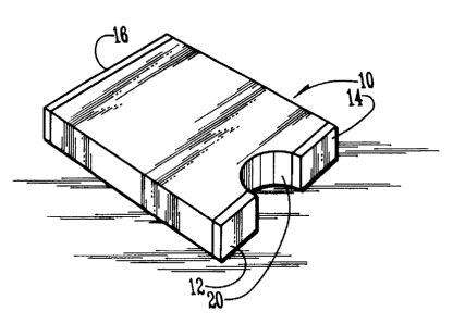
Referring to the drawings, the numeral 10 generally
designates the monolithic multilayer ultra thin chip inductor
of the present invention. Inductor 10 is a monolithic thick
film surface mount component. Inductor 10 includes two
terminals 12 and 14 located on the same end of inductor 10.
A third terminal 16 is a no-connect terminal located on the
opposite end of inductor 10.
The user of inductor 10 has the option of soldering only
the two terminals 12 and 14 to a circuit board, or to solder
all three terminals 12, 14 and 16 to the circuit board. The
no-connect terminal 16 makes no electrical connection with
the coil within inductor 10. By soldering only terminals 12
and 14, the mechanical stresses on the ceramic component 10
are reduced. The mechanical stresses are caused by thermal
expansion between component 10 and a circuit board to which
it is soldered. These stresses are reduced since terminals
12 and 14 are closer together than terminal 16 and either of
terminals 12 or 14.
If shock or vibration is more of a concern than the
stresses caused by expansion and contraction, the user may
solder all three terminals 12, 14 and 16 to the circuit
board. As a result, inductor 10 will be more rigid and
mechanically sound since it is soldered to the board in three
places and at both ends.
Another advantage of having terminals 12 and 14 located
at the same end of inductor 10 is that it allows for shorter
trace runs on the circuit board. The trace runs connect
terminals 12 and 14 to the other components soldered to the
circuit board.
As shown in Figures 3, 6 and 9, each coil layer consists
of one and one-half turns. Having one and one-half turns per
coil layer allows more coil turns per given thickness than
5
2186055
that allowed in the prior art. One and one-half turns per
layer is the preferred method of manufacturing inductor 10,
however, the number of turns per layer can vary. Less than
one and one-half coil turns per layer would allow for wider
traces increasing the current carrying capability, but as a
result, part of the reduced thickness advantage is lost, as
the overall thickness of the inductor must be increased to
reach the same inductance. In other words, if the same
thickness must be maintained, the maximum inductance
obtainable is less. If more than one and one-half turns per
coil layer are used, the thickness of the inductor required
for a particular inductance is decreased. However, the trace
width of the coils must be narrowed and the current carrying
capability of the inductor would be reduced. As a result,
one and one-half turns per coil layer are used for the
preferred embodiment.
A major advantage of the present invention is its small
size: The footprint of inductor 10 is often only 1/4 that of
the prior art. The preferred size is 0.375 inches in length,
0.25 inches in width, and 0.047 inches in thickness.
However, the present invention could be made to fit almost
any dimensions. The preferred size allows the part to be
thin enough to fit in PCMCIA cards including Type I PCMCIA
cards. Since PCM cards are small, the circuit board area is
at a premium and the height restrictions preclude the use of
though hole components. As a result, PCMCIA cards must use
surface mount technology.
The most important features of the preferred embodiment
are the superb electrical properties contained within such a
small package. Inductor 10 has a high inductance. It is
also very stable over a wide frequency range. The high
inductance stability from 100kHz up to 4MHz makes the part
excellent for use in DC to DC converters that typically
operate at 500kAz.
Inductor 10 has a Quality Factor (Q) which is much
higher than the prior art at frequencies in the 200kHz to
4MHz range. The low resistive losses creates the high Q.
6
CA 02186055 2005-03-24
The inductance stability along with i:he high Q, plus its 7MHz
BRF, combine to make the part operable at frequencies of at
least 2.5MHz.
The current rating and heat dissipation for inductor 10
are also excellent. At 500kHz, the theoretical rated current
that will generate a 20°C temperature rise at 25°C ambient is
near 0.6 amps. At 1 MHz, the theoretical current rating is
over 0.4 amps.
The structure of inductor 10 also makes it inherently
shielded. It has an effective core geometry similar to a pot
core. This results in low EMI radimting noise.
Another advantage of the present invention is its
ability to store a large amount of Eanergy compared to its
small size. As shown in Figure 14, the saturation of this
inductor is "softer" than comparably: parts. With typical
prior art inductors, the inductance drops sharply when
saturation occurs. In this case, h~~wever, the inductance
drops gradually as more current is ,agplied. This is
demonstrated by the inductor's continued ability to store '
~20 additional energy at higher D.C. current levels (see Figure
15).
Inductor 10 is manufactured using most of the methods
detailed in U.S. Patent X5,302,932 "Monolithic Multilayer
Chip Inductor and Method For Making Same",
"Electronic Thick
~ U.S. Patent No. 5,572,779
Film Component Multiple ~e~ninal arid Method for Making Same",
and patent application, Canadian Serial No. 2,158,784,
"Electronic Thick Film Component TE:rmination and Method for
Making Same".
While a single inductor ZO is shown in Figure 1, the
method for producing a plurality of inductors l0 is shown in
Figures 2-13.
Figure 2 shows the ferrite base or bottom cap layer 18.
The bottom cap layer 18 is printed until it reaches a
thickness that allows for an appropriate magnetic path. The
thickness is determined by the number of coils the final part
7
2186J55
will have. Figures 1-13 all show holes 20 formed on the
layers. The purpose of the holes is to form a separation
between the terminals 12 and 14 after the individual
components are cut apart (best shown in Figure 1).
Figure 3 shows the bottom cap layer 18 with a coil 22
having one and one-half turns printed on it. One end 24 of
the coil 22 extends to the edge of the component 10 and makes
contact to terminal 12 shown in Figure 1. The other end of
the coil 22 terminates at a location one and one half turns
from the first end. This end forms a connection end 26 which
will connect with a corresponding connection end of a coil on
the next layer.
A first ferrite layer 28 is then printed as shown in
Figure 4. The first ferrite layer 28 includes a via hole 30
for each individual component 10 and corresponds to the
connection end 26 of the bottom coil 22.
As shown in Figure 5, the via holes 30 are filled by the
first via fills 32.
Figure 6 shows the intermediate ferrite layer 28 with a
first intermediate coil 36 printed on it. The first
intermediate coil 36 has one and one-half turns, with one
connection end 38 corresponding to the connection end 26 of
the bottom termination coil 22 and a second connection end 39
corresponding to a connection end on the next layer. The
connection ends 26 and 38 are electrically connected by the
first via fill 32.
Figure 7 shows the second ferrite layer 40 which is
analogous to the first ferrite layer 28 shown in Figure 4.
In the same way, Figure 8 shows the second via fill 42 which
is analogous to the first via fill 32 shown in Figure 5.
Figure 9 shows the second ferrite layer 40 with second
intermediate coils 46 printed on it. The second intermediate
coils 46 each have one and one-half turns. The second
intermediate coil 46 has a first connection end 48
corresponding to the connection end 39 of the first
intermediate coil 36 and is electrically connected by the
second via fill 42. The other end of coil 46 has a second
8
218655
connection end 50 corresponding to a connection end on the
next layer. Additional coil layers may be added by repeating
intermediate layers shown in Figures 4-9 as needed depending
on the desired number of turns.
Figures 10 through 12 show three possible top
termination coils 52, 54, and 56. The top termination coils
are printed over an intermediate ferrite layer (such as
ferrite layers 28 and 40) and a via fill layer (such as via
fill layers 32 or 42). The top termination coils extend to
the edge of component 10 and are electrically connected to
terminal 14 (Figure 1). Either of the three top termination
coils may be used as discussed below.
The artwork for inductor 10 includes three different top
termination layers (Figures 10-12). Without three different
top termination coils, in order to increase or decrease the
number of coils in inductor 10, the number of coils would
have to increase or decrease by three turns. This would have
the undesirable effect of limiting the increments of coils in
inductor 10 to three.
When selecting the top termination coil, at least two
th:~ngs should be considered. First, the connection end of
th~s top termination coil must correspond to the second
connection end of the coil on the previous layer so that an
electrical connection can be made. For example, as shown in
the figures, first and third top termination coils 52 and 56
have connection ends 58 and 62 respectively. Connection ends
58 and 62 correspond to connection ends 50 (Figure 9) and 26
(Figure 3), but not connection end 39 (Figure 6). In other
words, first and third top termination coils 52 and 56 can be
used after bottom termination coil 22 or second intermediate
coil 46 (after first adding an intermediate ferrite layer 28
and a via fill layer 32), but not after first intermediate
coil 36. Similarly, second top termination coil 54 can only
be used after first intermediate coil 36 since connection end
60 corresponds with connection end 39 of first intermediate
coil 36. This same reasoning is used when selecting other
layer combinations. The second consideration is the number
9
2i86G55
of coil turns desired. For example, when choosing a top
termination coil, notice that the coils on first termination
coil 52 have one quarter turn while the coils on second and
third top termination coils 54 and 56 have three quarters,
and one and one-quarter turns respectively. The top
termination coils 52, 54, and 56 each have a termination end
64, 66, and 68, respectively, which each extends to the edge
of inductor 10 and is electrically connected to terminal 14
shown in Figure 1.
Inductor 10 is manufactured by layering the bottom
termination coil 22 (Figure 3j and one of the three top
termination coils 52, 54, or 56 (Figures 10-12j. Between the
bottom termination layer and the top termination layer, the
maker of inductor 10 has the option of layering no other
coils, first intermediate coil 36, first and second
intermediate coil 36 and 46, or first and second intermediate
coils 36 and 46 along with additional first and second
intermediate coils, etc., as long as the connection ends of
each individual coil correspond to the connection ends of the
coil below and above it so that an electrical connection can
be made by the via fills. Table 1 provides a guide to
possible combinations of coil layers and the resulting number
of coil turns.
It should also be understood that the terms "bottom" or
"top" do not necessarily mean that only the "bottom" layer
can be the first layer made in the manufacturing process.
The terms "bottom" and "top" were simply chosen to make
Figures 2-13 clear.
Because terminals 12 and 14 are positioned relative to
each other as shown in Figure 1, the total number of turns is
never a whole number. Inductor 10 always has a whole number
of coil turns plus an additional three-fourths of a coil.
Table 1 shows the coil layer progression needed to reach
a particular coil turn count. The table shows the inner coil
layers only and not the bottom cap 18 (Figure 2j or the top
cap (Figure 13j which is identical to the bottom cap 18.
Each combination of coil layers begins with the bottom coil
X186855
22 (Figure 3). After the bottom coil 22, either the first
intermediate coil 36 (Figure 6), the first top termination
coil 52 (Figure 10), or the third top termination coil 56
(Figure 12) can be printed. If the first top termination
coil 52 is printed on top of the bottom coil 22, an inductor
with 1~ coils is formed. If the third top termination coil
56 is added to the bottom coil 22, an inductor with 2~ coils
is formed. If the first intermediate coil 36 is added to the
bottom coil 22, then either the second intermediate coil 46
or the second top termination coil 54 can be printed. If the
second top termination coil 54 is printed, then an inductor
having 3~ coils is formed. If the second intermediate coil
46 is printed over the first intermediate coil 36, then the
maker has the option of next adding another first
intermediate coil 36, the first top termination coil 52, or
the third top termination coil 56. This pattern can be
repeated as shown in Table 1 to make an inductor having any
number of coils in increments of one.
After one of the three top termination coils is printed,
the cap layer 70 is printed until the part reaches the
desired thickness. The marks 21 are used to align the cuts
across the wafer to cut apart the plurality of components 10.
After the part is printed, each layer is dried at an
elevated temperature for several minutes. The preferred
drying parameters are ten minutes at 100°C.
After the final layer has been dried, the wafer is cut
into individual parts and then fired. The preferred firing
temperature is 900°C.
The magnetic material used to manufacture inductor 10
also contributes to the excellent electrical characteristics
that the present invention possesses. Preferably, inductor
10 is constructed of zinc, nickel, and Ni-Zn ferrite thick
film paste, manufactured by Heraeus, Inc., Cermalloy
Division, part No. IP9050.10.
The preferred embodiment of the present invention has
been set forth in the drawings and specification, and
although specific terms are employed, these are used in a
11
2i86~~5
generic or descriptive sense only and are not used for
purposes of limitation. Also, this invention applies to any
other electronic thick film components requiring a connection
between the inner conductors and the outer terminals of the
component.
Changes in the form and proportion of parts as well as
in the substitution of equivalents are contemplated as
circumstances may suggest or render expedient without
departing from the spirit or scope of the invention as
further defined in the following claims.
TABLE 1
Coil ~ Layers
Turns
1 3 4 BT,F1,V1,TT1
2 3 4 BT,F1,V1,TT3
3 3 4 BT,F1,V1,C1,F2,V2,TT2
4 3 4 BT,F1,V1,C1,F2,V2,C2,F1,V1,TT1
5 3 4 BT,F1,V1,C1,F2,V2,C2,F1,V1,TT3
6 3 4 BT,F'1,V1,C1,F2,V2,C2,F1,V1,C1,F2,V2,TT2
7 3 4 BT,F1,V1,C1,F2,V2,C2,F1,V1,C1,F2,V2,C2,F1,V1,TT1
8 3 4 BT,F1,V1,C1,F2,V2,C2,F1,V1,C1,F2,V2,C2,F1,V1,TT3
BT = Bottom Termination F1 = 1st Ferrite
Vl = 1st Via Fill C1 = 1st Intermediate Coil
F2 = 2nd Ferrite V2 = 2nd Via Fill
C2 = 2nd Intermediate Coil TT1 = 1st Top Termination
TT2 = 2nd Top Termination TT3 = 3rd Top Termination
12