Note: Descriptions are shown in the official language in which they were submitted.
21861~9
OPTICAL AMPLIFlER COMBINER ARRANGENlENT AND METHOD FOR
UPSTREAM TRQNSMlS~lON REALISED THEREBY
1 he preSQnt invention relates to an optical an,plifier co"lbiner
arrangemont as described in the pream~le of claim 1 and a method for
upstream lrans"~ission realised thereby, usecl in a tree-like optical network toperform upstroam transmission as descri~ed in the prea"~le of claim 10.
Such an optical a~ptifier combiner and such a method are already
known in the art, e.g. ~rom the article 'Ne~work Design for t~?e Information
Superh~ghwa~ written by P.W. France, J H. Mackenzie and others, published
10 by The European Instit~te for Communicat~ons and Networks in lhe book
ProcHedings volume 1 Papers on Br~adband Superhighway wherein p~ssive
op(ical networks are described which use such a combiner and which realiz~
such a melhod. These passive optical network systems are dovelopped to
meet the emerging superhighway requiremenls such as the capability to
provlde both existing narrowband ~nd new broadband distributive and
interactive services to serve both husiness and residential customers.
However serving business and residential customers requires a much
higher splitting factor than provided by these known networks. A main problem
in the realizatlon of high splitt~ng factors occurs during the upstream
20 transrnission. Indeed, due to this high splitting Factor a high powerbudg~t must
b~ ovelcome. The demanding optioal powerbudget for transmissi~n is
supported by the implementation ~f optical amplifiers in the deoqcated
branches However, due ~o the multiple access tec~,.,iq~Je used at the Optical
combiner which col"bi~,es the inror"-ation signals, all these optical an~pliriers
contribute to an a~cumulalion of ASE (amplified spontaneous e",issio") noi~e,
even when the optical amplifier does not carry an information signal and as a
resull thereof, the ASE noise can reach such an amplitude that the (,~.,s!"ittedsi~nals are degraded.
An object of the present inven~ion is to providn an optical amplifier
30 cornbiner arrangement and a method such as the above known on~s but which
2186149
~re slJIted for networks with high splitting factors, i.e. which ensure thflt the
transmitted signals can not be degraded by the relative~y high ~SE noise.
Accordin~ t~ the invention, tllis object is achieved by means of th~
optical amplifier combiner arrangement as described in claim 1, realizing the
method as descnbed in claim 10.
Indeed, since the branches whlch carry no information signal, ar~
interrupted with the c~ptical switches onloff, ~hese branches can not contributeto the accumulation of ASE noise at the opUcal cornbiner
A possit~l~ implementation of the control of the optical amplifier cor~biner
10 alrangement is that for each branch th~ ga~n value of the optical amplifier and
the optical switch onlc~ff are controlled respectively by means ot a first and
secon~ ~lectrical control signal. This implementation is described in claim 2.
The first electrical control signal is composed of gain setting data and gain
tunin~ data This gain tuning data is inlrocil~ced to comp~nsate deviations of
th~3 optical amplification due tu e.g. sensitiveness with r~sF)ect to temperature
and tlme of the optical amplifier.
An ~dditlonal characteristic f~ature of the present invenlion is that, as
described in claim 3, the switch onJoff is controlled by means of th~ second
el~ctrical control signal which results f~om the detection of the presence of an20 informatlon signal on the according branch.
Another way of contro~ling the switch onloff is described in claim ~, and
is based on the use, in an optical net.~ork uslng for upstream transmission a
time division multiple access techniquQ, ~ the detection of special grant
information ou~ of downstream irlrvlrl~atiOn The use of such speci~l grant
informatinn to realize time divisivn multiple access is well known in the art, e g.
from the publisched European patent appl~cafion wif~l publkafion r7~lmber EP-O
544 9,5 wherein a time sl~ management system Is described which allows
upstream transmission. The stream of station identities us~d therein is sinnilarto th~ ~pecial ~rant information. In the impl~r"en~alion of claim 4 the second
- 2~8~9
elec~rical control signal is deterrnined by the detection of special granl
informalior1 in downstream ir~ tiorl.
Yet a further ch~racteristic feature of the present invention is th~t, as
described in claim 5, the gain settin~ data i~ d~ten~,:aed by measurir~g the
power of the information signal.
Another characteristic feature of the present invention is th~, as
described in claim 6, the gain tuning data is determined by measurin~ the
power of ~he amplified inrorn~alion signal .
An al~orn~tive way to d~tsrmine the gain tuning data is descri~ed in
10 claim 7 and consists in using a memory means ~o ",e,l,ori~e lhe value Of the
l~st measured powor of an amplified signal and to use this value to contml ~he
gain tuning data ~or a followlng tran~mitted Information signal.
Another way to determine the gain tun~ng data is described in claim 8,
which introduces a power level unit lo measure the power level o~ the outgoing
optical signal to determine the gain tuning data for the b,~nches carrying an
informaUon signal. In thls way, Instead of measuring the pow~r for each
dedicated branch, only one pvwer rn~asurement has to be p~,fb""ed wliich is
less power consumins~
Still another character,stic feature is the integration of the dptical
~0 combiner with all optical switches on/off In one optical switch, as descri~ed in
claim 9.
~ he above mentloned and oth~r objects and ~eatures o~ the invention will
become moro apparent and the invention itself will be best understo¢~ by
ref~rrin~ to the following description o~ an embodimen1 taken in conju~ction
with th~ accompanying dr~wing
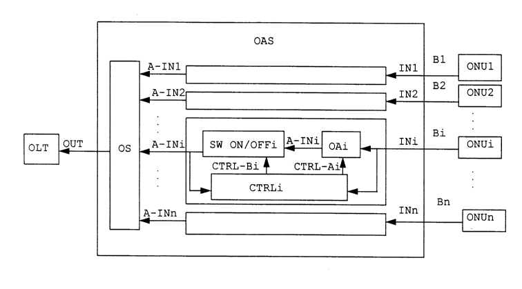
First, the optical amplifier c~mbiner arrangen,ent OAS will be explained
by me~ns of a functional deseril tion of the blocks shown in the flgure. Based
on this de~cription. impleme, It~tion of the ~unetional blocks in the figure ~ill ~e
obvious to a person skille~ in the art.
- 21~ 9
The optical amplifier combiner arran~ement OAS~is used in a tr~e-lilce
optical network consisting of the cascade conne~lion of dedicated branches
B1, B2, ..., Bi, Bn and of Ihe optical amplifier combiner a"~"~",ent OAS and
of a common branch. The optic~l amplifier combiner arrangement OAS is
coupled b~tween a plurality of optlcal network ~Jsers ONU1, ONU2, , ONUi,
, ON~Jn and an optical line tetminalor OLT via the above mentioned
dedicated branches and cornrnon branch respectively.
The optical amplifier co",~i. ,er arrangement OAS includes for e~ch
branch e g Bi, of the dedicated branchQs B1 B~, ., Bi, . ., Bn two basic p~rts .10 - an optical ~n)~l-fier OAi coupled to the respectivs nctwotk user ONUi of the
optical net~ork u~ers ONU1, ONU2. , ONUi, .., ONUn; and
- an optical switch onloff SW ON/OFFi coupled between the optical an~plifier
OAi and an optlcai combiner O~
The optical combiner OS is coupled between all optical switch~s onloff
SW ONIOFF1, SW ON/OFF2. . ., SW ONlOFFi ... SW ONlOFFn which are
simular to the optical switch on/off SW ON/OFFi and the optical line t~rminator
OLT
the optical amplifier con,bil1er arran~ement OAS enables upsltre~m
transmission in the optical network o~ informotion signals IN1, IN2, , ll~li, ,
20 INn fro~ the optical network users ONU1, ONU2, , ONUi, ..., ONUn to the
optlcal llne termlnator (:)L I .
The principle working of the optical amplifier combiner OAS will be
explained in the following para~raph with respect to a signal INi ~lansn~itled
over a branch ~i, the working with respect to the other branches being
idenlical .
the optical ampli~ier OAi amplifies INi wi~h a ~ain value Gi (not shown)
and generates thereby an amplif~cd inf~rmation signal A-lNi ~Ath a
predeterrnined power level
- 21~ 9
The optical switch on/off SW ONlOFFi passes the amplified info",.ation
signal A-lNi when it is present~ but inlerrupts the branch Bi whsn the amptifiedinformation signal A-lNi is not present.
The optlcal combiner OS combines all amplified information signals A-
IN1 A-IN2, ., A-lNi, .., ~-INn simular lo Ihe amplifi~d in~r~ tion si~nal A-lNi
according to a multiple access technique and genorates thereby an outl3oing
optical signal OUT for a,~plication to the optical line terrninator OLT
In this ernbodiment ~he working o~ the optical amplifier OAi and the
optical switch on/of~ SW ON/OFFi of each branch Bi is controlled by means of
10 control means CTRLi. The control m~ans CTRLi is co~pled to the OAi ar~d the
optical switch onloff SW ONlOFFi and controls:
- ~h~ ~ain value Gi by means of a first Cl~ l ical control signal C~-AI
comp~secl of gain setting data GSi (not shown) and gain tuning ~iata G~i (not
shown), and
- the switch onloff SW ONtOFFi by means of a second electrical control signal
CTRL-Bi.
The gain setting data GSi the gain luning data GTi and the second
electrical conlrol signal CTRL-Bi can be determined in different ways. A few
particulàr implcmentations to determine them are described in a functional way
20 in the following par~ylaphs, but they are not shown in the figure to avoid
overloading thereof
To dctermine the second electrical control signal CTRL-Bi, fo~ each
branch Bi, the control means CT~Li further includ~s power detectic~n me~ns
which via an optical tap draws off the illfo""~ sign~l INi a small po~4er part.
Th~ power detection means determines whether the information s~nal INi is
present o~ is not present and determines the second ele~trica~ control 8i~nal
CTRL-Bi as a result thereof.
To deternline the gain setting data GSI, ~or each branch Bi, the control
means CTRLi Further includes power measuring means. The same optic~l tap
- 218~1~9
as above is use~ and the power rr~easuring means meas~r~s the po~ver of the
nformation signal INi and determines the gain setting data GSi based the~reon.
It has to be noted t ere that ~o en~ure that tho power measurin~ rneans
has enou~h time to fulfil its function an optical del~y line (not sllown) is
coupled botween the optical tap and the optical amplifler (:)Ai. The optical
delay line delays the inf~r",dlion signal INi ~Intill the optical ampiifier pAi is
adjusted.
To detotmine the gain tuning data GTi for each branch Bi tho control
means CTlRLi furth~r includes addilional power measuring means. Via an
10 additional optical tap coupled between the optical switch on/off SW O~ FFi
and ~he optical combiner OS a small power part is drawn off the amplified
inf~r",dlion signal A-INI and the a~ditional power measuring means measures
the pownr of the amplified information signal A-lNi and detormines the ~ain
tuning data GTi based lhereon.
Furthermore it is notod th~t although for the optical amplifier OAi an
erbium doped fibre am~lifier is used semiconductor optical amplifiers ar~ vety
good candidates to use in this implementalion because o~ their low swit~h-on
tirne. It is also remarked that these s~rniconductor optical amplifiers can be
used to integrate the functions o~ the oplical amplifier OAi and of the optical
~?() switch on/off ~;W ON/C)FFi
An alternative implementation to detennine the second electrical c~ntrol
signal CT~L-Bi is realised for ~ptical networks ~Ivhere the optical combiner OS
combines the amplified infe""dtion si~nals ~-IN1 A-IN2 ... A~ i ... A-lNn
according to a time division multiple access techniqu~. For such an aptical
n~twork the optical arnplifier combiner al,ange",ent OAS includes ~n optical
network terminator NTOAM (not shown) for performing operation and
maintenance func~ions. T'l~ NTOAM is coupled tO Ule optical line terrnlnator
OLT by means of also an additional optical tap, and to the control r~eans
CTP<Li. The addi~ional optical tap draws off the do~",sl,ea"~ signals which are
3u sent from th~ optical line ler,n;nator OLT to the optical network terminators
21~
ONU1, ONU2, ., ONVi, .... ONUn a small po~ ,all and pro~.rides this power
fraction to the optical network terminator NTOAM which captures special grant
i.~f~"",~tion out of these downstream signals. Accor~i"sJ to the remark in the
introduction, th~ use ~f special grant information to realize time di~rision
mu~tiple ~ccess is well known in the art. With this special ~rant information, the
optical network terminator NTOAM knows ~xactly when an information signal
INi will be sont by an optical network user ONUi and when the i,~ né1tion
si~nal INi wi~l b~ applled to the optical amplifier OAi. The special grant
information is appliecl to the control means CTRLi which is now able to
10 dotermine whether the information signal INi will be present or willl not be
present within a predetermined time intQrval and determines the sec~nd
electrical control signal CTRL-Bi as a result ~hereof.
Still ano~h~r alternative implementation to d~(~r",i,-~ the gain tuning data
GTi, fur each blanch Bi, is realised by inclu~ing in th~ control means CTRLi,
additional t~ measuring means to measure the power o~ an amplified
Inlormation ~ignal A-lNi. also memory means to mernorize the value of the
measured power of the amplified si~nal This value is us~d to determin~ the
gain tunin~ data GTi for a following transmitted info",1ation signal INi.
Finally. it h~s to ~e remarked that an alternative way to determin~ the
20 gain tuning data G~i, for each ~ranch Bi, is realized with the implementation of
one power level unit. The power level unit, included in the opt~cal amplifier
combiner arrangement OAS, is co~Jpled between a control output of the optical
combiner OS and the control means CTRLi asso~idted with each branch Si.
rhe power leYel unit measures the power l~vel of 1he outgoing optical ~i~nal
OUT and provides the result thereof by means o~ electrical power level d~ta t~
thQ control means CTR~i. Th~ control means CTRLi is now able to d~ler,-,ine
the g~in tuning data GTi if an information signal is pr~sent.
It has to be remarked thal the optical combiner OS and all optic~l
swilctles onloff SW OI~J/OFF 1, SW ON/OFF2, ..., SW ONlOFFi. ..., SW
- 218~1~9
ON/OF~n simular to the optical switch on/off SW ON/OF~i can be integrate~ in
one oplical switc~l.
Sir1ce it is obvious for a p~3rson skilled in the art how lo realize the above
alternative implernenta ions based on their fundional description these
realizations are not clescribed in further details.
It has als~ to be remarked that the outgoing optical signal OUT of Ihe
present optical amplifier combiner ~rran~ement OAS has to be anlplified in
order to overco",e a longe distance to the optical line terminator OLT. With an
effici~nt workin~ of the diHerent optical amplifiers OA1 OA2~ . OAi ..., OAn
10 simular to the optical amplifier OAi in the optical amplifier ~ombiner
arr~ngement OAS and an appropriate access ~utocol that assures continuous
u,~sl,ean~ trans",ission for the outgoing signal OUT the outgoing optical ~i~nalO~Jr has no longer a bursty character like the infu,l,-blion ~ignals IN1 IN2 ...INi INn ~1ave In this way a fast gain setting optical amplifier Is no longer
required for the amplifica~ion of thc optical out~oing ~igna~ OUT and a st~ndardoptical amplifiers can be us~d
While the principles of the inventien have been d~scribed abo~Je in
connection with specific apparatus it is to be clearly understood t~a~ Ihis
description is made only by way of example and not as a limitation on the
20 scope of the invention.