Note: Descriptions are shown in the official language in which they were submitted.
218b339
WO 95127371 PCTlUS95/03754
DATA SEGMENT DRIVEN AFC LATCH
FOR BI-PHASE STABLE FREQUENCY PHASE LOCKED LOOP
This invention relates generally to digital data receivers and
particularly concerns a digital television signal receiver. A number of
systems have recently been proposed for transmitting and receiving
television signals in a digital form. The television signal may comprise, for
example, a compressed wideband high definition television (HDTV) signal or
one or more compressed National Television System Committee (NTSC)
signals. The two most widely promoted modulation techniques being
considered for effecting such transmissions are quadrature amplitude
modulation (C1AM) and vestigial sideband modulation (VSB). U.S. Patent
No. 5,087,975 discloses a VSB system for transmitting a television signal
in the form of successive M-level symbols over a standard 6 MHz television
channel, with a relatively small (low level) pilot at the lower edge of the
channel. while the number of levels M (i.e., the VSB mode) characterizing
the symbols may vary, the symbol rate is preferably fixed, such as at a rate
of 684 H (about 10.76 Megasymbols/sec.), where H is the NTSC horizontal
scanning frequency. The number of symbol levels used in any particular
situation is largely a function of the signal to noise (S/N) ratio
characterizing
the transmission medium, a smaller number of symbol levels being used in
situations vvhere the SIN ratio is low. It is believed that a system
accommodating symbol levels of 24, 16, 8, 4 and 2 provides adequate
flexibility to satisfy most conditions. It will be appreciated that lower
values of M can provide improved SIN ratio performance at the expense of
reduced transmission bit rate. For example, assuming a rate of 10.76
Megasymbols/sec., a 2-level VSB signal (1 bit per symbol) provides a
transmission bit rate of 10.76 Megabits/sec., a 4-level VSB signal (2 bits
per symbol) provides a transmission bit rate of 21.52 Megabits/sec., and so
on.
CA 02186339 1999-06-03
L
Proper,operation of a digital television receiver
requires the received carrier signal to be acquired
relatively rapidly and the gain of the radiofrequency
(RF) and the intermediate frequency (IF) sections to be
appropriately adjusted. Carrier acquisition in QAM
receivers is relatively difficult because of the absence
of any sort of pilot. While the use of a pilot in the
above-mentioned VSB system greatly facilitates carrier
acquisition, some difficulties may nevertheless be
encountered due to the relatively low level of the pilot
and the limited pull-in range of synchronous demodulators
used in VSB receivers. One aspect: of the invant;nn
enhances pull-in of the frequency and phase locked loop
(FPLL) and another deals with an improved automatic gain
control (AGC) system. Also, the FPLL in the synchronous
demodulator is bi-phase stable. Consequently, the phase
of the output data maybe inverted and therefore need to
be phase reversed. Further, the lock-up characteristics
of the FPLL are determined by the characteristics of the
automatic frequency control (AFC) filter and in another
aspect of the invention, an improvement in such
characteristics is provided. The present invention is
directed to a segment driven AFC latch for stabilizing
the FPLL.
In particular the invention provides a method of
operating a receiver including a bi-phase stable
synchronous demodulator responsive to a received signal
to recover data and a DC pilot component therein, said
data being formatted in successive data segments, with
each data segment including a sync character, said method
including the steps of deriving data segment sync
information including a sign bit from the recovered data
and using said sign bit to augment said DC pilot
component.
2
CA 02186339 1999-06-03
Further the invention provides a television receiver
for receiving a digital television signal formatted in
repetitive data segments, including sync characters and a
pilot component, said receiver including sampling means
for recovering data and said DC pilot component from said
television signal, synchronous demodulator means
including a bi-phase stable phase locked loop, locked by
said DC pilot component, for controlling said sampling
means, phase inverting means for reversing the phase of
said recovered data, means responsive to said sync
characters for producing a sign bit indicative of the
polarity of said recovered data, means for operating said
phase inverting means when said sign bit indicates an
improper polarity, and means responsive to said sign bit
for stabilizing said bi-phase stable phase locked loop.
Additionally the invention provides an apparatus for
demodulating a digitally encoded modulated signal
including a demodulator responsive to said digitally
encoded modulated signal for producing a demodulated
output signal having either a first polarity or a second
opposite polarity, said demodulated output signal
including a DC pilot component, means for determining the
polarity of said demodulated signal, and means responsive
to said determining means for augmenting said DC pilot
component.
In the Drawings:
FIG. 1 is a partial block diagram of a receiver
constructed for receiving an M-level VSB signal;
FIG. 2 is a more detailed showing of the IF
amplifier an synchronous demodulator of FIG. 1;
2a
W0 95127371 PGTIUS95I03754
FIG. 3 is the circuit for controlling the AGC for the receiver;
FIG. 4 depicts the operational modes of the AGC circuit;
FIG. 5 discloses a data polarity inverter for automatically phase
' inverting the data, if required;
FIG. 6 is a segment lock driven AFC latch in accordance with
the invention; and
FIGS. 7A and 7B are curves illustrating operation of the filter of
FIG. 6.
As mentioned above, the transmitted VSB signal preferably includes
a small pilot at the lower boundary of the 6 MHz television channel, which
is converted to an intermediate frequency (IF) of about 46.69 MHz near the
upper boundary of the channel. Also, although not limited thereto, the
transmitted signal preferably comprises successive data frames each
including 313 data segments. Each data segment includes 832 symbols
(occurring at a rate of about 10.76 Megasymbols/sec.), 828 of which are
used for data and 4 of which are provided in a fixed position of each data
segment for defining a segment sync character. The data segment sync
character comprises only 2-level symbols, while the data symbols may be
2, 4, 8, 16 or 24-level depending upon the application. Also, the first data
segment of each frame comprises a sequence of 2-level symbols
representing a frame synchronization code and a VSB mode control signal
identifying the level M (24, 16, 8, 4 or 2) of the data symbols of the
remaining 312 data segments of the frame.
The pilot may be conveniently developed in the transmitter by
introducing an offset (constant DC level) to the symbol values. In the
receiver the offset generates a constant DC which is used for carrier
recovery. In accordance with orie aspect of the invention, this "recovered"
DC in the receiver is eliminated from the data channel, after carrier
acquisition, to optimize further processing.
3
W0 95127371 PCTIUS95/03754
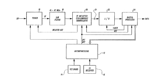
Referring to FIG. 1, the received RF signal is converted to an IF
signal by a tuner 10, which is controlled by a microprocessor 12.
Microprocessor 12 is responsive to user inputs, from either a keyboard 14
or an IR receiver 16, for applying appropriate signals to tuner 10 for tuning
the selected channel. The IF signal, including the pilot at 46.69 MHz, is
applied from tuner 10 through a SAW filter 18, having a pass-band of
about 41-47 MHz, to an IF amplifier and synchronous demodulator 20. The
analog baseband output of demodulator 20 is coupled via a capacitor 21 to
an analog to digital (AID) converter 22, which samples the signal and
provides the M-level symbol information in binary form to a digital
processor 24. Capacitor 21 eliminates the DC offset mentioned above
from the AID 22 input. As will be explained in further detail hereinafter,
AID 22 is operated for sampling the output of demodulator 20 at the
correct symbol times in response to a clock signal generated by digital
processor 24. Digital processor 24 supplies the data and also supplies an
AGC control signal to IF amplifier and synchronous demodulator 20 which,
in turn, supplies a delayed AGC signal to tuner 10. Both demodulator 20
and digital processor 24 are responsive to an AFC Defeat signal generated
by microprocessor 12 in response to selected start-up conditions, such as
power-up, channel change and loss of data segment or frame
synchronization. Finally, since the phase of the data output may be
inverted because the FPLL in the synchronous demodulator is bi-phase
stable, an automatic arrangement for providing the proper phase of data is
also included. This is described more fully in connection with FIG. 5.
IF amplifier and synchronous demodulator 20 is shown in more
detail in FIG. 2. The IF signal from SAW filter 18 is applied through a gain
controlled amplifier 30 to one input of an IF switch 32. The gain of
amplifier 30 is~controlled by an AGC control and charge pump 31. circuit
31 is responsive to Gain-Up and Gain-Down signals for charging and
discharging a capacitor 33 to a desired value for controlling the gain of
4
218~~~9
VJO 95127371 PC1YUS95I03754
amplifier 30. Circuit 31 also generates a delayed AGC signal for application
to tuner 10.
A crystal oscillator 34 is enabled in response to the AFC Defeat
signal from microprocessor 12 for applying a relatively strong signal at the
frequency of the pilot (46.69 MHz) to a second input of IF switch 32. IF
switch 32 is also responsive to the AFC Defeat signal for coupling the
output of crystal oscillator 34 to the switch output and is otherwise
operable for coupling the output of IF amplifier 30 to its output. Thus the
output of IF switch 32 is the IF signal when the AFC Defeat signal is
absent, and is the output of crystal oscillator 34 when the AFC Defeat
signal is present.
The output of IF switch 32 is applied to the first inputs of a pair
of multipliers 40 and 42. A voltage controllable oscillator (VCO) 44
nominally generates an output at a frequency equal to 4 x pilot frequency
(i.e. 186.76 MHz), which is applied to a divide-by-four prescaler circuit 46
for producing a pair of 90' phase-displaced signals at the pilot frequency.
The in-phase (O') signal is applied to the second input of multiplier 40 to
produce an in-phase baseband component I and the quadrature (90') signal
is applied to the second input of multiplier 42 to produce a quadrature
baseband component Q. The I and Q components are coupled through
respective low-pass filters 50 and 52 to remove second and higher order
harmonic mixer products, and amplified by respective amplifiers 54 and 56
.to provide desired output levels. The amplified I and Q
components are supplied to respective inputs of an FPLL 58, which is
operated, in a well known manner, for generating a tuning voltage Vt for
locking the frequency and phase of the signal generated by VCO 44 to 4
times the pilot frequency. Capacitor 21, as mentioned above, prevents the
DC offset in the I channel signal from being applied to AID 22. In this
manner, the quadrature signals produced by divider 46 are locked to the
pilot IF frequency for appropriately demodulating the received IF signal.
WO 95127371 pCT/US95103754
During certain start-up types of conditions, such as during
power-up or a channel change, the frequency of VCO 44 may be so far
from its nominal frequency of 186.76 MHz that rapid lock-up by FPLL 58 in
response to the relatively small received pilot cannot occur. (FPLL 58
typically has a pull-in range of only about ~ 100 KHz at the IF frequency
with the weak pilot signal, whereas its pull-in range with a strong signal is
typically about t 750 KHz.) To alleviate this problem, the relatively strong
46.69 MHz output of crystal oscillator 34 is applied through IF switch 32
to the inputs of multipliers 40 and 42 during an initial interval, which is
defined by the duration of the AFC Defeat signal, i.e. AFC Defeat signal is
enabled, rather than the received IF signal from IF amplifier 30. The initial
interval comprises a fixed period (approximately 200 milliseconds (ms) long)
of maximum gain. It will be appreciated that it takes about 1 ms to bring
the gain to maximum--this is considered part of the initial interval. During
the initial interval corresponding to the AFC Defeat signal duration, the IF
amplifier gain is held at its maximum level, irrespective of the actual level
of the IF signal. Thus during the interval, the AGC system is overridden.
A relatively strong signal, at the frequency of the IF pilot is applied to
the synchronous demodulator from crystal oscillator 34, during the initial
interval to allow FPLL 58 to rapidly bring the frequency of VCO 44 to its
nominal value. After the initial interval, as determined by the absence of
the channel data signal is continually compared to a maximum value or
clipping level by a comparator 72. If the absolute value of the received
data signal exceeds the clipping level for eight consecutive symbols,
decoder 68 generates an output causing decoder 70 to generate a Gain-
_ Down signal for reducing the gain of amplifier 30 by a predetermined
amount or increment. This continues as long as the condition required by
comparator 72 is satisfied. For periods when the condition is not
satisfied, no gain reduction occurs. When segment sync lock is attained,
decoder 68 is disabled and the receiver enters the coherent AGC mode of
6
wo 9s~z~sn
PGT/US95/03~54
operation wherein the gain of amplifier 30 is controlled according to the
strength of the received IF signal, for example, as determined from the
segment sync character, which is represented by the correlated pulse
produced at the output of filter 62. The correlated pulse is applied to a
polarity selection circuit (shown in FIG. 5) to assure that the data polarity
is correct since FPLL 58 can lock up in either of two phases.
As will be seen, a polarity invert control (FIG. 5) which is
developed in response to the correlated pulse and a polarity selection sign
bit, is used to control the polarity of polarity inverter 59 and the position
of a switch 73 which applies a ground voltage (zero) or a +5V voltage to
the FPLL circuit in FIG. 6, as will be described. This feature involves the
present invention.
A reference Level is subtracted from the correlated pulse in a summer
76 and the result is integrated in an AGC integrator 74, the output of which
is applied to decoder 70 for controlling charge pump 31. In particular,
when the integrated output of summer 76 exceeds a first level, a Gain-
Down signal is generated by decoder 70 to reduce the gain of amplifier 30
and when the integrated signal falls below a second level a Gain-Up signal
is generated by decoder 70 to increase the gain of amplifier 30. Integrator
74 is reset by decoder 70 after a Gain-Up or a Gain-Down signal is
generated. The output of summer 76 is also applied to a segment sync
integrator 94, the output of which is applied to one input of a comparator
96, the other input of which is supplied with a zero signal reference. The
output of comparator 96 is supplied to a segment sync generator 98 for
providing a segment sync output whenever the integrated correlation pulse
from filter 62 is equal to or greater than a zero value and the segment sync
lock signal when segment sync lock has been attained.
The segment sync generator 98 develops a segment sync lock
signal when a sufficient number of segment syncs have been found (which
may be accomplished by using a confidence counter arrangement) and the
7
2186~~9
WO 95/27371 PCTIUS95103754
segment sync lock signal is conveyed to the FPLL in FIG. 5. As will be
seen, the polarity invert control, the segment sync lock signal and the
absence of the AFC Defeat Signal are used to accomplish the present
invention of latching the AFC for the FPLL.
The non-coherent AGC operation is relatively fast, being able to
effect a gain change every eight symbol clocks. Coherent AGC operation,
on the other hand, is responsive to the segment sync character and can
thus effect a gain change only once per data segment. It will be
appreciated that coherent mode AGC may be responsive to any signal
characteristics and this invention is not to be limited to the use of segment
sync to develop the AGC voltage.
As mentioned, FPLL 58 in synchronous demodulator 20 (FIG. 2)
is bi-phase stable. Consequently, the phase of the output data may be
inverted. The polarity inverter 59 in digital processor 24 inverts the phase
of the data signal, if necessary. Polarity inverter 59 is controlled by the
polarity invert control from the polarity selection circuit (FIG. 5).
In F1G. 5, the sign bit of the correlated sync pattern produced at
the output of filter 62 is coupled to the D input of a first flip-flop 82,
whose
Q output is coupled to the p input of a second flip-flop 84 and to one input
of a comparator 86, whose second input is supplied with the Q output of
flip-flop 84. The
output of comparator 86 is applied to the Reset input of a 3-bit counter
88, whose Carry output is coupled to one input of an AND gate 90. A
second input of AND gate 90 is supplied with the Q output of flip-flop 82
and the output of the gate is coupled to the toggle input of a toggle flip-
flop 92. The Q output of flip-flop 92 comprises the polarity invert control
signal which controls the operation of polarity inverter 59. Flip-flops 82-
84 and counter 88 are docked by the segment sync signal derived from
segment sync generator 98 (FIG. 3).
8
W 0 95127371 PCT/CT595103754
The sign bit of the correlated output of filter 62 will be logic 0
when the output of synchronous demodulator 20 is properly phased. If the
sign bit is logic 1, inverter 80 will be operated to invert the polarity of
the
data signal applied to digital processor 24.
More specifically, flip-flops 82 and 84 are operated for storing
the sign bits of successive outputs of sync correlation filter 62. Logic 0
and logic 1 sign bits result in flip-flop states of Q=0 and Q=1,
respectively. If the sign bit does not change (i.e. no output from
comparator 86) for 8 successive segment sync characters, the output of
counter 88 enables AND gate 90 for checking the polarity of the current
sign bit. If it is not logic 0, i.e. the state of flip-flop 82 is Q=1, AND 90
will produce an output for toggling flip-flop 92, thereby causing polarity
inverter 59 to change state. If the sign bit was logic 0, AND gate 90 does
not produce an output and the state of inverter 80 is unchanged.
FIG. 6 shows the preferred embodiment of FPLL 58 (FIG. 2) which is also
responsive to the AFC Defeat signal from microprocessor 12 and to the
latch arrangement of the present invention as described hereinafter. The
FPLL conventionally includes an AFC filter 80 comprising a series of
resistors R1, R2 and R3 and capacitors C1, C2 and C3. The input of filter
80 is connected for receiving the demodulated I channel data signal and its
output is connected to a first input of a limiter 82, the ,second input of
iimiter 82 being supplied with a reference voltage via a resistor 88 that is
coupled to a potentiometer 91. The output of limiter 82 is supplied to one
input of a multiplier 84. The demodulated Q signal is supplied to a second
input of multiplier 84, whose output is connected to a PLL filter 86, which
generates the voltage Vt for controlling VCO 44 (FIG. 21.
It will be seen that, in accordance with the present invention,
the second input of limiter 82 is also connected through a resistor 92 tc a
closed terminal (C) of a switch 94 that is operated in response to the
segment sync lock signal. The movable element of switch 94 is connected
9
2186339
H'O 95/27371 PC1YUS95I03754
to another switch 100 that is operated in response to the AFC defeat signal
and which is supplied from switch 73 in F1G. 3. It will be recalled that
switch 73 couples either a t 5V or a OV (ground) depending upon the lock
up polarity of the bi phase stable FPLL 88. The arrangement of the multiple
switches in series precludes the FPLL from being latched until segment lock
has been achieved and the AFC defeat signal is inactive. The result is that
the pilot augmentation circuit of the invention is immediately disabled in
response to a channel change, an on/off switch operation, etc.
AFC filter 80 has amplitude and phase versus frequency
response characteristics as shown in solid line in FIGS. 7A and 7B,
respectively, for (1y rejecting the high frequency data components in the I
channel data signal and (2) providing a phase shift of the input signal. An
error in the frequency of VCO 44 from its nominal demodulating frequency
is reflected in the production of beat frequencies in the I and Q signals. As
long as the beat frequencies are not excessive, i.e., the frequency of VCO
44 is within a given range of the nominal demodulation frequency, AFC
filter 80 will produce an output of sufficient amplitude and phase to allow
for correction of the VCO frequency. Such correction is effected by
multiplying the limited output of AFC filter 80 with the O signal to supply a
frequency correction signal to PLL filter 86. With reference to FIGS. 7A
and 7B, it will be noted that as the beat frequency increases, the amplitude
of the AFC filter response decreases and the phase shift imposed
thereby approaches 180'. Both of these factors reduce the effectiveness
of AFC filter 80 to make the necessary frequency correction. In particular,
when the phase shift of the filter exceeds 180', the frequency of VCO 44
is actually pushed in a direction opposite from that required to achieve
frequency lock. During conditions of receiver turn on, channel change or
loss of signal, the frequency of VCO 44 can be sufficiently different from
its nominal frequency to make acquisition of the received signal very
W 0 95/27371 PCTlUS95I03754
difficult, even when the FPLL is operated in response to the output of
crystal oscillator 34.
The foregoing problems are overcome by providing a charge
pump 88 which is enabled by the AFC Defeat signal for injecting a current
into the output node 90 of AFC filter 80 in response to the I signal. This, in
effect, modifies the amplitude and phase response characteristics as shown
in dotted line in FIGS. 7A and 7B. It will be seen that the modified
amplitude response provides a more gradual roll-off in the amplitude
response of the filter with increasing frequency and in the phase shift. The
phase shift, more importantly, is essentially fixed at about 90' for
increasing frequencies and never gets to 180'. Thus, AFC filter 80
provides an increased level output signal having a phase shift of less than
180' (i.e., about 90') to facilitate carrier acquisition in response to the
output of crystal oscillator 34 during the initial interval.
The present invention is thus seen to provide improved performance
of the acquisition circuitry (FPLL 58) which develops a small DC voltage in
response to the pilot in the received signal. It will be recalled that prior
to
acquisition, the AGC system is operated at maximum gain which magnifies
the DC pilot and aids in the acquisition of frequency lock. During normal,
coherent, operation of the AGC (after segment sync lock has been
attained), the IF gain is reduced from what it was in the beginning of the
initial interval and so is the DC pilot. The various circuit elements in the
analog demodulator 20, of which FPLL 58 is a part, can introduce DC
voltages which may offset the small DC pilot. Also the data symbols are
multi-level level and could adversely influence the lock stability of the FPLL
by diminishing the magnitude of the DC pilot developed at the output of
filter 80. In some cases, the data or spurious DC voltages in the
demodulator 20 may overcome the DC and result in loss of lock or
introduction of data dependent phase modulation of VCO 44. This is
precluded in the present invention by clamping or latching the AFC when
11
21~6~~9
wo 9sn737i
PCTIUS95/037s4
segment sync lock has been attained by supplying a (relatively) large
augmenting DC voltage to the pilot DC, thus preventing unlocking of the
FPLL due to data or spurious DC voltages in the chip. Either a +5V or a
ground potential is applied to the second input of limiter 82 when segment
sync lock has been attained by switches 94 and 100. The determination of
+ 5V or ground is made by the detected sign bit from sync correlation filter
62. The sign bit is determinative of the polarity of the data and the pilot.
The FPLL is bi-phase and can lock up with either pilot polarity and whatever
polarity of DC it locks to is reinforced with the inventive arrangement.
It is recognized that numerous changes in the described
embodiment of the invention will occur to those skilled in the art without
departing from the invention. The invention is to be limited .only as defined
in the claims.
12