Note: Descriptions are shown in the official language in which they were submitted.
~ ~ 8 ~ 5
WO 95/26566 PCT/US94/13759
SPUTTERING TARGET EROSION PROFILE
CONTROL FOR COLLIMATED DEPOSITION
The present invention relates to sputter deposition,
and particularly to the design and use of sputter coating cathode
assemblies, particularly magnetron sputtering cathode assemblies,
for use in collimated deposition.
Background of the Invention:
In sputter deposition processes, a great deal of
attention has been historically paid to the thickness uniformity of
the deposited film. In many commercial scale processes for
applying sputter coated films to the surfaces of semiconductor
wafers, particularly those in which a high rate of deposition is
also a consideration, magnetron enhanced plasma generation and
plasma shaping are employed to establish an erosion profile of the
sputtering target that assists in providing the desired distribution
wo ss/~6s66 2 1 ~ 65aS PCT I 594/13759
of target material consumed on the target surface and desired
distribution of film deposited on the wafer substrate.
More recently, users of sputter coating equipment for
the production of semiconductor wafers have deemed it desirable
to use, and manufacturers of such equipment has deemed it
desirable to provide, sputter coating target and cathode
assemblies in which rotating magnet packages are used to provide
the magnetron enhancement of the ion producing plasma for use
in the sputter coating process for removal of the sputter coating
material from the target. One such rotating magnet sputtering
target and cathode assembly is described and illustrated in U.S.
Patent No. 5,130,005 entitled MAGNETRON SPUTTER COATING
METHOD AND APPARATUS WITH ROTATING MAGNET
CATHODE, hereby expressly incorporated herein by reference.
In the design of sputtering cathode assemblies, it has
been recognized that the uniformity of the film deposited on the
surface of a substrate is improved by making the target large with
respect to the surface of the substrate being coated.
Theoretically, with all other parameters being equal, an infinitely
large target with a uniform erosion profile is capable of
overcoming coating non-uniformity that is due to the presence of
less of the sputtering source near the edge of the substrate than
there is near the substrate center. There are, however, practical
WO 95/26566 ~ 1 8 6 ~ 5 PCT/US94/13759
- 3 -
limitations on the sizes of sputtering targets. Usually, a
compromise is made by coating circular wafer substrates by
providing a target that has a diameter about one-third or one-half
larger than that of the wafer being coated. Nonetheless, with this
compromise, a uniformly eroded target will result in the deposition
of a coating that is progressively thicker moving from the rim of
the substrate toward the center.
In the manufacture of cathode assemblies, the designs
have been optimized to shape the erosion profiles of the targets
to compensate for the thinner edge coating effect and other
factors contributing to lack of uniformity of the sputtered film
being deposited. This design optimization is commonly carried
out by selectively configuring the magnet assemblies used to
shape the plasma. To overcome the thinness of the coating at
the edge, magnet assemblies are often designed to produce a
stronger magnetic field to trap more plasma around the edge of
the target, which causes the target to erode at a higher rate near
the edge to compensate for the lesser target area near the rim of
the substrate.
An additional consideration arises when the wafers
being coated are not flat smooth surfaces on which the film is to
be deposited, but are stepped, having micron size vias with walls
perpendicular to the surface of the wafer. In certain applications,
- 4 - ' 2`~ 86~05
it is sought to apply the spu;tered coatings on the bottorns of the
vias, which are shadowed by the vias' stepped sides. In such
applications, it becomes a goal to apply the coating of a sufficient
thicicness on the bottoms of the vias before excessive coaling is
deposited on the vias stepped sides. In some applications, this
goal is pursued by providing a collimator between the target and
- the semiconductor wafer to restrict the amount of shallow angle
particles impinging on the wafer from the target. By providing a
coilimator, the angle of incidence of sputtered material moving
from the target toward the substrate is restricted to angles nearly
perpendicular to the target, whereby the deposition rate on the
sides of the vias is reduced, while the rate of coatin~ material
deposited on the via bottoms by particles moving perpendicular to
the target and wafer is not materially retarded.
European Patent Application 0440377 describes a
sputtering apparatus in which a colllmator is provided
between the target and the substrate to be coated. The
collimator cells have a length to diameter ratio of 1:1 to
3:1. The target has a greater lateral extent than the
substrate. The particles are said to be emitted from the
target in substantially uniform manner.
With the use of a collimator between the target and
the substrate being sputter coated, size of the target in relation to
the wafer has a different effect than it does with sputtering
arrangements in which collimators are not being used. As a
consequence, a sputtering cathode design, optimized to produce
uniformity in a non-coliimated application, no longer performs
- AMENDED SHEEI-
IPEA/EP -'
2 1 8 6 5~ ? 5
~~ optimally with the collir~ato~ AS ~ fesult, the bottoms of vias on
some parts of the wafer become coated at different rates, and to
different film thickness, than those at other parts of the wafer. It
has been found by applicants that an ideal cathode assembly for
use in a non-collimated application tends to result in excessive
deposition near the edge of the wafer substrates and insufficient
deposition remote from the edge and nearer the center of the
wafer.
In attempting to improve sputter coating uniformity in
collimated sputter coating applications, some have embarked on a
trial and error modification of sputtering cathode assemblies.
While some such attempts have produced an improved result with
a particular collimator being used, the improvements tend to be
lost when the design of the collimator is changed. In fact, it has
been found that over the life of a collimator or over the life of a
sputtering target, the improved effects of such haphazard
approach to cathode assembly design has been found to
dissipate.
One cause of film uniformity changes over the life of a
collimator or target has been found by applicants to be the
collimator design parameter referred to as the aspect ratio. A
collimator is usually regarded as a grid like structure interposed
between the target and the substrate having an array of holes
therethrough for the passage of particles. The holes in the
collimators have some size or dimension such as a hole diameter,
where the holes are round, or an equivalent dimension where the
- AMENDED SHE~T
-IP~A/EP ~
W095/26S66 2 1 8 6 5 Q 5 PCT/US94/13759
holes are otherwise shaped, such as hexagonal or square. The
collimator also has a thickness, which is the dimension through
the hole in a direction normal to the target and substrate along
which a particle must pass to move from the target to the wafer
surface. An aspect ratio of a collimator is usually defined as the
ratio of the collimator thickness to the effective diameter of the
collimator holes. The higher the aspect ratio, the greater the
collimating effect that is produced by the collimator in restricting
the particles to those that are generally moving from the target to
the substrate in a direction normal to the collimator, and hence to
the surface of the substrate, which is typically parallel to the
collimator.
The change in aspect ratio over the life of the
collimator, referred to above, has been found to occur at least in
part because the wide angle particles that do not pass through
the collimator holes are rather blocked by the web or grid
structure that forms the side walls of the collimator holes, tends
to coat the sides of the holes of the collimator, causing the holes
to narrow. Thus, cathode assemblies that are optimized to
produce an erosion profile that results in acceptable film
uniformity deposited by a collimated source having a particular
aspect ratio have been found by applicants to cease to be
optimized as the collimator is used.
WO 95/26566 PCT/US94/13759
2~ ~-6~D~
- 7 -
Furthermore, the greater the film thicknesses being
deposited, the greater is the rate at which the collimators become
coated to the point that they are no longer suitable for their
applications. Cathode assembly designs that work for only a
specific or narrow range of collimator aspect ratios are less useful
for depositing materials to great thicknesses, and thus have been
limited to use with only very thin films such as barrier layers of,
for example, titanium or titanium nitride.
There is a need for a sputtering cathode design,
particularly a systematic criteria use in configuring the magnetron
and other plasma shaping assemblies of a sputtering cathode
design, so that uniformity in the film applied using collimated
sputtering sources, particularly having collimators of a range of
contemplated collimator designs, is maintained. There is further a
need to overcome the above described problems to extend the
utility of collimated sputter coating to more materials, and to
otherwise render collimated sputter deposition more efficient and
more effective.
SummarY of the Invention:
An objective of the present invention is to provide a
cathode assembly that produces an erosion profile for a sputtering
target which, if used with a collimator, provides uniform film
deposition .
21:86~
It is a further objective of the present invention to
provide a cathode assembly for a sputter coating apparatus that
will provide uniform film deposition when used with a collimator
having an aspect ratio that falls within a wide range.
More particular objectives of the present invention are
to provide a cathode assembly design that is effective to provide
-
uniform collimated deposition as the aspect ratio of the collimator
varies over the course of its use.
A sputtering method in accordance with the
invention comprises the steps of providing a wafer support
for holding a circular wafer centered on an axis, providing
a sputtering target formed of sputtering material, having
a circular outer rim centered on the axis, and having a
sputtering surface spaced from, parallel to and facing the
support, providing a collimator centered on the axis space~
from, between and parallel to the target and the support,
and having an aspect ratio of at least 0.5, the aspect
ratio being the ratio of the thickness (T) of the
collimator to the width of the cells of the collimator,
shaping with magnet assembly means positioned behind the
target a plasma adjacent the sputtering surface of the
target characterised in that the plasma is shaped such as
to produce an erosion profile on the sputtering surface of
the target that includes an annular peripheral area of
maximum erosion adjacent the rim of the target and an
interior area radially inward of the peripheral area of
generally uniform erosion that is less than the maximum
erosion and greater than half of the maximum erosion.
A sputtering cathode assembly in accordance with
the invention comprises a wafer support for holding a
circular wafer centered on an axis, a sputtering target
formed of sputtering material, having a circular outer rim
centered on the axis, and a sputtering surface spaced from,
parallel to and facing the support, a collimator centered
on the axis spaced from, between and parallel to the target
and the support, and having an aspect ratio of at least
AMENDED SHEFT
IPEA/EP
~ 2i a6505 ~ `
-8a-
0.5, the aspect ratio being the ratio of the thickness of
the collimator to the width of the cells of the
collimator and magnet assembly means positioned behind the
target and configured for shaping a plasma adjacent the
sputtering surface of the target characterised in that the
magnet assembly is configured for shaping the plasma to
produce therewith an erosion profile on the sputtering
surface of the target that includes an annular peripheral
area of maximum erosion adjacent the rim of the target
and an interior area radially inward of the peripheral area
of generally uniform erosion that is less than the maximum
erosion and greater than half of the maximum erosion.
In accordance with the principles of the present
invention, there is provided a method of and apparatus for eroding
a sputtering target so as to form an erosion groove profile which
is substantiaily uniform in an interior area of the target with a
deeper, preferably asymmetrically gaussian shaped, enhancement
near the outer edge of the target. In accordance with a preferred
embodiment of the invention, the erosion profile provided by the
method and apparatus of the invention has a relatively deep
enhancement area near the outer edge of the target, a specified
and shallower erosion area near the center of the target, and an
intermediate annular area that is flat to a prescribed degree
between the center and the edge areas.
Further in accordance with the present invention, a
cathode assembly as set forth above is provided, in a sputter
coating apparatus, in combination with a collimator of aspect
AMENDED SHEET
I~ P
W0 95/26S66 2 l ~Q S PCT/US94/13759
ratios of greater than approximately 0.5, and in the preferred
combination, with aspect ratios of at least approximately 1.0, and
preferably in the range of from 1.0 to at least 2Ø
Further in accordance with the preferred embodiment
of the present invention, the cathode assembly includes a rotating
magnet assembly, which in conjunction with a sputtering target,
forms an erosion groove profile as described above.
The method and apparatus of the present invention
provide uniform film deposition when used with collimators over a
wide range of aspect ratios.
The present invention provides the advantages of
improving the film thickness uniformity achievable with a
collimator by modifying the shape of the erosion profile produced
in the sputtering target. In addition, the invention provides a
range of target erosion profiles, including specific profiles, which
will perform with a range of collimator aspect ratios. Further, the
invention provides a target erosion profile which will perform in a
more consistent manner as the targets erode deeply and the
distance from substrate to sputter surface changes.
These and other objectives and advantages of the
present invention will be more readily apparent from the following
detailed description in which:
WO 95/26566 2 ~ 8 6 5 o 5 PCT/US94/13759
- 10-
Brief DescriDtion of the Drawings:
Fig. 1 is a diagram illustrating a typical non-collimated
sputtering target and wafer arrangement.
Fig. 2 is a diagram iliustrating the sputtering target of Fig. 1
in combination with a collimator of relatively low aspect ratio.
Fig. 3 is a diagram similar to Fig. ;2 but illustrating a
collimator of higher aspect ratio.
Fig. 4 is a diagram similar to Fig. 3 but illustrating a
collimator of still higher aspect ratio.
Fig. 5 is a graph representing an equation describing a target
erosion profile for use without a collimator.
Fig. 6 is a graph similar to Fig. 5, but representing an
equation describing a target erosion profile for use with a
collimator having an aspect ratio Iying within an extended range.
Fig. 7 is a graph illustrating uniformity measurements made
after introducing collimators into sputtering devices employing
cathode assemblies producing the erosion profile of Fig 5.
Fig. 8 is a graph, similar to Fig. 7, plotting uniformity
measurements made with a target in accordance with the erosion
profile of Fig 6.
Detailed Description of the Preferred Embodiments:
In the sputter deposition of a thin film of uniform
thickness across a substrate, there is a known geometrical
relationship between the degree of uniformity, the substrate size,
WO 95/26566 ~ ) 5 PCT/US94/13759
._
- 11 -
the spacing between target and substrate, and the specific shape
and size of the erosion profile in the target. However, it has been
found that, when a collimating structure is interposed between
.~
the target and substrate, which is frequently done in order to
improve the coating of three dimensional features on the
substrate surface, and particularly to improve the sidewall and
bottom step coverage of sub-micron features, the resulting
uniformity is significantly changed. Additionally, as the aspect
ratio of the collimator changes over the course of the use of the
collimator, or by operator selection to satisfy application
requirements, film thickness uniformity changes. As such, the
best uniformity achieved is generally not as good as the
uniformity possible without a collimator when the target erosion
profile was developed for non-collimator performance.
The reason for this effect is illustrated in Figs. 1-3.
Fig. 1 diagrammatically illustrates a cross section through the
center of a circular target 10. Plotted on the target 10 is an
erosion profile 12 representing the relative rates at which material
is sputtered from various points across the diameter of the target
10. The profile 12 illustrated is representative of the profile
produced when the cathode is designed according to parameters
established for use of the target 10 without a collimator. Typical
points 13 and 14 on substrate 15 both "see" the entire target
21 86505
WO 9S/26566 PCT/US94/13759
area without restriction. Points such as point 13 near the edge or
rim 16 of the target 10 see less target than points such as point
14 more central on the target 10, and thus will receive less
sputtered material unless the areas of the target 10 closer to it
are sputtered at a greater rate. Profile 12, to produce the same
film thickness at all points on the surface of the substrate 15, is
designed to have a deeper erosion groove 18 near the target edge
16. Such a design is an attempt to approximate a theoretically
perfect uniformity that would result from a target of theoretically
infinite diameter sputtered to a uniform profile.
Fig. 2 diagrammatically illustrates the effect of a
collimator 20 with a low aspect ratio of about 1. The aspect ratio
is defined as the ratio of the thickness Tto the width W of a
collimator cell 21. With such a collimator 20, the view from the
points on the substrate 15, such as point 14 for example, are
limited by the sidewalls 22 of the cells 21 to a maximum angle 24
through which the collimator sees a corresponding area 25 of the
target 10. Point 13, which is at the edge of the wafer 13, sees
the target 10 through an angle 26, equal to the angle 24.
However, because the target 10 only partially fills the field of
view spanned by the angle 26, the point 13 sees a smaller area
28 of the target 10 than the area 24 seen by point 14. Because
the collimator sidewalls 22 shadow part of the target 10 from the
21 8~05
WO 95126S66 PCT/US94/13759
- 13 -
points 13 and 14, each points receives less coating material in a
given amount of time than the same points would receive in the
non-collimated case of Fig. 1. With the profile 12, the collimator
affects the points 13 and 14 differently. For example, the
deposition rate may be reduced more at point 13 than at point
14, resulting in a difference in uniformity of the deposited film
between points 13 and 14 on the substrate 15.
Fig. 3 diagrammatically illustrates the effect of another
collimator 30 having a relatively high aspect ratio of about 3. The
areas seen by points 13 and 14 on the wafer 15, for example
areas 31 and 32, respectively, become more restricted by
sidewalls 34 of the collimator 30, and thus are smaller than the
areas 25 and 28 of Fig. 2. With the same erosion profile 12, the
result of the collimator 30 will be an even greater difference in the
film coating uniformity between points 13 and 14 than resulted
from the collimator 20 of Fig. 2.
Fig. 4 diagrammatically illustrates the effect of another
collimator 40 having an even higher aspect ratio of about 4. The
areas seen by points 13 and 14 on the wafer 15, for example
areas 41 and 42, respectively, are even more restricted by
sidewalls 4A of the collimator 40 than the areas 31 and 32 of
Fig. 3. With the same erosion profile 12, the result of the
collimator 40 will be an even greater difference in the film coating
WO 95/26566 2 1 8 6 5 Q 5 PCT/I~S94/137~9
- 14-
uniformity between points 13 and 14 than resulted from the
collimators 20 of Fig. 2 and 30 of Fig. 3. With the collimator 40,
however, both of the areas 41 and 42 lie entirely on the surface
of the target 10, and thus, the deep erosion groove 18 is counter-
productive, as will be seen from the discussion below.
In cases of collimated sputter deposition, ideal
uniformity is theoretically achieved with a uniformly eroded target
of a radius that is the radius of the substrate plus Wd/t, where d
is the target-to-substrate distance. W/t is the collimator hole
width-to-thickness ratio, which is the reciprocal of the collimator
aspect ratio. For non-collimated sputter deposition, ideal
thickness uniformity is achieved with a uniformly eroded target of
infinite diameter. With realistic targets of limited actual size, it
becomes necessary to modify the erosion to produce non-uniform
depths which compensate for the limited size of the target. This
follows the general form of deeper erosion, illustrated by the
groove 18 in Figs. 1-4, near the edge of the target 10, but with
significant differences of shape between erosion grooves
optimized for use with and without collimators.
A simplified definition of such a shape is provided by
the equation:
W09S/26566 2 1 8 ~ ~ Q5 PCT/US94/137S9
- 1 5 -
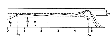
Equation (1):
y(x)=aO~IO e
for x s xO
and
( J _(X-X0)2
for x > xO
Where: y = Erosion intensity;
x = Distance from target center;
xO = Radius to peak depth of erosion groove;
aO = Minimum Erosion Intensity for x s xO.;
/0 = Amplitude of enhanced erosion groove from aO.;
tr = Half width of enhanced erosion groove.
Equation (1) is illustrated in Fig. 5, which plots the resultant
shape as a level, uniform erosion in the central area of the target,
enhanced by a gaussian shaped deeper zone or erosion groove
near the edge. For non-collimated sputtering sources, with
targets that are about one-third to one-half larger in diameter than
the wafers being coated, aO is typically about 20% of lO.
Because of variables in such things as the
characteristics of target materials, gas scattering of sputtered
particles, sticking coefficients of sputtered particles and the actual
WO 95126566 2 1 B ~ 5 ~5 PCT/US94/13759
magnet construction and other parameters producing the target
erosion, the more fully descriptive equation creates an envelope
of erosion shape which permits fine turning for the variables.
Fig. 6 illustrates the envelope developed from the use of
Equation (2).
Equation (2):
x--x
y (xJ = Ice c
for x ~ xc;
_ (_ ) 2 ~ X--Xo ~ 2
y(xJ=m +i0 Ii e l +Ioe l
1 0 for XC ~ x :~ xO;
( x--xO ) a
for X 2 Xo~
Where:
m = Minimum erosion intensity on flat part, i.e., for
XC 5 x ~ xO, and
m + 1O = 1.O. Also:
_ ~ X-Xi ) 2 = Intensity fluctuation on flat part .
where:
I; = Fluctuation peaks < ~n-m~;
Z'1'86~'D5
WO 95/26566 PCT/US94/13759
_
- 17-
xO = Radius to edge erosion
groove;
x; < xO;
a; = Half width of peak i.
~ O J 2
IOe l = Edge intensity enhancement for x < xO.;
where:
a1 = Half width of peak erosion
on the inside of the edge
erosion groove.
0 X-Xo 2 Edge intensity for x ~ xO.,
O as x~ co;
where:
a2 = Half width of peak erosion
on the outside of the edge
erosion groove.
I e ( oc ) = Erosion intensity at target center area;
where:
m ~ lc c n,
/c = Max intensity of center
area,
XC = radius of center area.
WO 95126566 :2 1 `~3 6 ~ 0 5 PCTIUS94/13759
In the above equations, the units of measure and
constants, such as the "half widths" ~r, are somewhat arbitrary
and will be selected based on factors such as magnet structure in
the course of the optimization procedure explained below. Based
on the selections and adjustments of parameters, the optimization
is carried out to derive an envelope, represented by the values m
and n, which define the relative erosion depth of the internal flat
portion to the depth of the peripheral groove, and the maximum
fluctuation of the erosion peaks within this portion.
Fig. 7 plots the performance of a standard erosion
groove designed for producing +/- 5% uniformity without a
collimator when used with collimators of various aspect ratios,
while Fig. 8 plots the improvement of this invention using an
erosion profile in accordance with Equation (2).
In accordance with the present invention, when a
target is to be used with a collimator, a computer model is
constructed representing the geometry of the target, wafer and
collimator, in a manner similar to the diagrams of Figs. 1-4,
described above. Assuming, for example, a circular target, a
circular collimator and a circular wafer all centered on the same
axis, and given a target diameter, a wafer diameter, a collimator
aspect ratio, a target to wafer spacing, and a wafer to collimator
spacing, a computer iteration is performed, using any one of a
2 1 86505
WO 95126566 PCT/US94/13759
- 19 -
number of suitable numerical methods, to determine the amount
of target area that each point on the wafer "sees". The resulting
calculation represents the distribution of coating on the wafer that
would result if a uniform target erosion profile were employed.
Then, in accordance with the method of the present
invention, an erosion profile represented by Equation (2) is
introduced. With each point on the surface of the target
weighted by the value y~x) that results by solving the equation of
Equation (2) for a point of radius x from the target center or axis,
a numerical iteration is performed to minimize the maximum
differences among the target areas, weighted by the erosion
profile of Equation (2), seen from the points on the wafer surface.
Equation (2), as used in the method as described
above, is a tool for use in arriving at the parameters needed for
the design of a cathode assembly that will produce the desired
erosion profile. The equation is particularly suitable for design of
circular magnet designs, particularly rotating magnet assembly
that rotates on an axis that aligns with the axis of the target-
collimator-wafer assembly. Calculation of the optimized erosion
profile produces the parameters m, n, and 1;, including /c- These
parameters, for example, may be used to adjust the strengths of
magnets in the magnet assembly. The selection of the radii xO, x;
and xc of the peaks may be selected based on achievable magnet
~ 86505
-- - 20 -
assembly geometry, and may be also varied in the optimization
process. In addition, the parameters a" a2 and ac are preferabiy
also optimized in the calculation process. These parameters
affect both the geometry and strengths of the magnets of the
magnet assembly.
-
Applying the above method, the following sets forthexamples of erosion profile parameters that have been derived
following Equation (2), in which the relative erosion intensity y, as
a function of the distance x from the target center or axis:
1 0 Examale:
~o 3 c~
For a wafer of diameter Dw =L(8 inches~ the target will
typically have a diameter r = (1.2 to 1.5J x Dw,, for example, in
~q ~c~
the range of ~11.5 inche~. The target to wafer spacing with such
~ 6 cw.
wafer and target dimensions will be preferably of~3")to
1o ac~ C~
approximatelyl(4.0" - 4.5") (i.e., 3/8 - 1/2, or 3/8 to 9/16 Dw )-
Further, the wafer to collimator spacing in such a configuration
3~ '~ 1' 4 4~ C~--
will be from approximatelyL~.25~ to 1.75n)(approximately 3/16
Dw). Then, for collimator aspect ratios of from approximately 1.0
to 2.0, the parameters for designing a magnet assembly or for
otherwise controlling the erosion profile of the target are:
m = 0.6
n = 0.75
I; < ~n-m = 0.15J
AMENDED SHEET
- ~PEA/EP '
21 86~
WO 95/26566 PCT/US94/13759
- 21 -
~1 0 45 ; cr2 ~ 0.25"; ac 0.25"
XC < 0.25"
In the above example, the area of the target inward of
the peripheral groove at xO is eroded to about half or more of the
maximum depth of the peripheral groove, and preferably to
between 60% and 75% of the depth of the peripheral groove.
The ratios may be smaller with collimators of lower aspect ratios
and greater with collimators of higher aspect ratios, but
significantly greater than the ratio of about 20% that is
characteristic of the shallower central erosion employed with non-
collimated sources.
In the example, the above listed values of the
parameters will provide generally uniform deposition of +/- 5%
on the wafer with collimators of aspect ratios ranging from less
than 1.0 to more than 2Ø The uniformity with such collimators
will be provided where the target, wafer and collimator
dimensions and spacings vary somewhat from those used in the
example.
The above calculated erosion profiles have been
implemented in, and are particularly suitable with, magnet
assemblies such as disclosed in U.S. Patent No. 5,130,005
entitled MAGNETRON SPUTTER COATING METHOD AND
o ~ . ? 1 ~ O 5
- 22 -
APPARATUS WITH ROTATING MAGNET CATHODE, which is
expressly incorporated herein by reference herein.
The method set forth above provides erosion profiles
that are useful in combination with collimators having aspect
ratios of from 0.05 to 5Ø The cathode assembly design set
forth above is particularly suitable for collimator aspect ratios of
about 1.0 that may vary to up to approximately 2Ø The profiles
of such cathode assemblies are particularly capable of replication
with rotating magnet assemblies, which in conjunction with a
sputtering target, form erosion groove profiles so derived.
AMENDED SHEET
IPEA/EP