Note: Descriptions are shown in the official language in which they were submitted.
CA 02186506 2004-03-12
64159-1483
PHASE-LOCKED SYNC STR3PPER
GOVERNMENT R_1GHTS
The U.S. Government has a paid-up license in this invention and the right in
limited circumstances to require the patent owner to license others on
reasonable terms
as provided for by the terms of Contract No. F33657-89-C-0009 awarded by the
United States Department of the Air Force.
~je-ld of the Invention
The invention relates to video signal processing and more particularly to a
method and apparatus for stripping synchronization information from a
composite video
signal.
A composite video signal contains synchronization (sync) information encoded
on it. A display processor uses sync to create a phased lock pixel clock. This
allows the
display processor to generate synthetic symbols. The sync format may be any
one of
several different compositions, however, in many circumstances the output sync
format
must not change regardless of the input format. To accomplish this desired
output, the
display processor must strip sync off without affecting the rest of the video
signal.
Most prior art sync strippers generally comprise up to four matched diodes or
transistors which require the video to be properly do biased. Circuits of this
type
generally have associated high impedances which require buffering into and out
of the
circuit. The prior art devices are also temperature sensitive, which require
complex
temperature compensating networks.
U.S. Patent No. 5,140,422 to Constable is a prior art solution to removing
sync
from the composite video signal. There are several problems with the Constable
implementation. The National Television Standards Committee (NTSC) (composite)
video signal must be delayed with respect to the N_SYNC signal which is
created by the
NTSC video. A delay circuit is damaging to the quality of the video. Delay
circuits
have low pass filter characteristics; that is, they are band limiting so high
frequency
components, such as edges and lines, etc., will become fuzzy or disappear
completely.
Delay circuits also add in noise and generally are not usable over temperature
extremes.
WO 95127366 a ~ PCT/US95I03954
_2_
Furthermore, Constable as disclosed will not work. The control signal N_SYNC
preferably goes high slightly after the video sync interval has ended.
Therefore, the
signal must be delayed with respect to itself then the signal must be made to
last longer.
The delay circuit is disclosed but Constable fails to teach how the signal can
be made to
last longer.
U.S. Patent No. 4,379,309 to Berke et al. describes the matched diode or
transistor embodiment as described above. The circuit is a very complex non-
linear
circuit that is not stable over temperature, or production lots of transistors
or diodes.
This circuit is an amplitude limiter which has all the problems of an
amplitude system,
which include temperature compensation, non-linearity and parasitic problems.
U.S. Patent No. 4,464,679 to Wargo describes using a phase-locked loop (PLL)
and composite sync to hook up to a microprocessor interface for a video
system. Wargo
teaches detecting sync and does not disclose sync stripping.
U.S. Patent No. 5,189,515 to Chen describes the use of a PLL to eliminate
1 S equalization pulses and noise from the composite sync signal after the
sync signal has
been detected. Chen discloses a PLL to generate horizontal and vertical sync
signals
using digital techniques by separating the horizontal and vertical signals
from the
composite sync signals. Chen does not teach using the PLL to strip the
composite sync
signal off the composite video signal.
Delay lines are used in the prior art to make the current pulse width
completely
blank the composite sync. A signal of any width occurnng anywhere with respect
to the
sync is disclosed by using a PLL. As a result of using the PLL instead of
delay lines, a
much higher quality, high bandwidth video can be processed. Additionally,
contrary to
the prior art devices, the present invention is temperature independent.
SUMMARY OF THE INVENTION
In accordance with the present invention there is provided an apparatus and
method for stripping the synchronization (sync) component from a composite
video
signal. The preferred circuit for stripping a sync component from a composite
video
signal comprises a phase-locked loop (PLL) for creating a high frequency
clock, phase-
locked with a video sync signal, and for generating a signal that encompasses
the video
sync signal, and an analog switch controlled by the signal that encompasses
the video
sync signal for stripping the video sync signal from the composite video
signal.
WO 95/27366 ~ PCT/US95/03954
-3-
The preferred PLL comprises a circuit for determining a leading edge of the
video sync signal. An alternative embodiment of the PLL comprises a circuit
for
determining a trailing edge of the video sync signal.
The preferred signal that encompasses the video sync signal comprises a
circuit
for starting the signal at a first time period prior to the video sync signal
and ending the
signal at a second time period after the video sync signal. The preferred
embodiment
comprises a circuit for making the time periods selectable. The preferred time
periods
are longer than an activation time for the analog switch.
The signal that encompasses the video sync signal further comprises an analog
switch activation time. The preferred time periods are also longer than 1 of
frequency
the high frequency clock.
The preferred analog switch comprises a switchable input operational
amplifier.
The analog switch can also comprise an analog multiplier.
The preferred analog switch comprises a circuit for switching a blank level
voltage onto the composite video signal. The analog switch alternatively
comprises a
circuit for stripping horizontal sync. The analog switch can also comprise a
circuit for
stripping vertical sync.
The preferred circuit for stripping a synchronization component from a
composite video signal comprises a phase-locked loop comprising a 10 MHz clock
phase-locked with a leading edge of a video sync signal, and a signal that
encompasses
the video sync signal comprising a circuit for starting the signal, 1 clock
oscillation
before a leading edge of the video sync and ending at approximately 50 clock
oscillations thereafter, and an analog switch comprising a switchable input
operational
amplifier controlled by the signal, for switching a blank level voltage onto
the
composite video signal.
The preferred method of stripping a synchronization component from a
composite video signal comprises the steps of creating a high frequency clock,
phase-
locked with a video sync signal and for generating a signal that encompasses
the video
sync signal, controlling the signal that encompasses the video sync signal
with an
analog switch, and stripping the video sync signal from the composite video
signal with
the analog switch.
WO 95/27366 ~ ~ PCT/US95/03954
_4_
The preferred step of creating comprises determining a leading edge of the
video
sync signal. The alternative step of creating comprises determining a trailing
edge of
the video sync signal.
The preferred step of generating comprises starting the signal that
encompasses
the video sync signal at a first time period prior to the video sync signal
and ending the
signal that encompasses the video sync signal at a second time period after
the video
sync signal. An alternative embodiment comprises selecting the time periods.
The preferred step of generating a signal that encompasses the video sync
signal
comprises selecting time periods that are longer than a time for the analog
switch to
activate. The preferred step of generating a signal that encompasses the video
sync
signal further comprises determining an analog switch activation time.
The preferred step of selecting time periods comprises providing a time period
longer than - of the high frequency clock.
frequency
The preferred step of providing an analog switch comprises providing a
switchable input operational amplifier. The alternative step of providing an
analog
switch comprises providing an analog multiplier. The preferred step of
providing an
analog switch comprises switching a blank level voltage onto the composite
video
signal. The alternative step of providing an analog switch comprises stripping
horizontal sync. Another alternative step of providing an analog switch
comprises
stripping vertical sync.
A primary object of the present invention is to provide a sync stripper
without
matched diodes or transistors.
Another object of the present invention is to strip a sync signal from a
composite
video signal regardless of its composition.
A primary advantage of the present invention is that it does not require do
biasing.
Another advantage of the present invention is that it is not temperature
sensitive.
Other objects, advantages and novel features, and further scope of
applicability
of the present invention will be set forth in part in the detailed description
to follow,
taken in conjunction with the accompanying drawings, and in part will become
apparent
to those skilled in the art upon examination of the following, or may be
learned by
W095/27366 ~ ~'~ PCT/(1595/03954
practice of the invention. The objects and advantages of the invention may be
realized
and attained by means of the instrumentalities and combinations particularly
pointed out
in the appended claims.
The accompanying drawings, which are incorporated into and form a part of the
specification, illustrate several embodiments of the present invention and,
together with
the description, serve to explain the principles of the invention. The
drawings are only
for the purpose of illustrating a preferred embodiment of the invention and
are not to be
construed as limiting the invention. In the drawings:
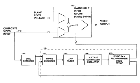
Fig. 1 schematically illustrates the preferred embodiment of the invention;
Fig. 2 illustrates three different composite video signals and the sync
stripper
signal prior to implementation; and
Fig. 3 illustrates the signals of Fig. 2 after implementation of the preferred
embodiment.
1FSCIZ1PTION OF TI-IE P FFFRRF MBODIM NT
The video sync stripper apparatus and method of the present invention comprise
hardware components to strip a sync signal from a composite video signal
without do
biasing the video signal and containing reduced temperature sensitivity. As
indicated in
Fig. 2, the sync component of various types of video signals such as those
utilized in the
broadcast industry, military applications and industrial applications, can be
stripped
with this invention. This invention is useful in a variety of applications
such as
television video systems, synthetic video applications or other video
applications
requiring removal of a video sync component.
Fig. 1 illustrates the preferred embodiment of the present invention.
Composite
video input 112 is sent to sync detector 100, such as a voltage comparator, or
the like,
which are commonly known in the art. The output of sync detector 100 is then
input to
phase-locked loop (PLL) 114.
PLL 114 consists of phase detector 102 which compares the phase between the
detected sync and the sync generated by the loop 114. Phase detector 102
generates an
error which is proportional to the phase difference of the detected sync and
the
generated sync.
WO 95/27366 PCT/US95/03954
'~ ~ ~'D-
-6- _.
Loop filter 104 is a low pass filter which converts the error from the phase
detector 102 into a voltage which drives voltage controlled oscillator 106.
Voltage controlled oscillator 106 generates a high frequency clock signal that
is
synchronous with the detected sync.
The high frequency clock is then divided down by a programmable logic
apparatus 108 which creates a signal with a frequency and phase similar to the
detected
sync. This signal is feedback to phase detector 102 to complete the PLL 114.
In the preferred embodiment, the PLL 114 is configured to "lock on" the
leading
edge of the sync signal; however, an alternative embodiment can be configured
to "lock
on" to the trailing edge.
The programmable logic apparatus 108, such as an ALTERA 5032
(manufactured by ALTERA), generates a signal that starts before the leading
edge of the
composite sync and lasts longer than the trailing edge of the composite sync,
as shown
in Figs. 2 and 3. This is accomplished by counting the nqmber of clock
oscillations
from the first leading edge of the sync signal to the trailing edge. In an
alternative
embodiment, the number of clock oscillations are counted from the first
trailing edge of
the sync signal to the next trailing edge. In selecting the time periods, or,
inversely, a
clock frequency, the time periods must be longer than ' . The time periods
frequency
before the leading edge and after the trailing edge can be varied by the
programmable
logic apparatus 108 by varying the number of clock oscillations before the
leading edge
of the sync signal, and the number of clock oscillations to end the generated
signal.
This signal is sent to the switchable input operational amplifier (op-amp)
110, such as a
BURR-BROWN OPA 676 (manufactured by BURR-BROWN) (or an analog switch),
which switches in a blank level voltage or other selected voltage, rather than
allowing
the sync signal to pass.
In determining the time period generated by the programmable logic apparatus,
the switching time of the switchable input op-amp 110 must be taken into
consideration
as well as variations in the sync signal. For example, a standard video sync
signal is
approximately 4.7 micro seconds long or corresponds to about 47 clock
oscillations for
a 10 MHz clock. If switchable input op-amp 110 requires 6 nano seconds to
switch, the
generated signal from the programmable logic apparatus 108 must start 1 clock
64159-1483 CA 02186506 2004-03-12
oscillation before the sync signal leading edge and last at least ~ micro
seconds or 50
clock oscillations. Although a switchable input op-amps 110 is disclosed, any
other
high speed, low glitch switch, which is known in the art can be used.
In yet another alternative embodiment, the PLL 114 detects both the leading
edge and the trailing edge of the sync signal with the programmable logic
apparatus 108
generating a signal that encompasses the sync by counting clock oscillations
as
discussed above.
The present invention can also strip either horizontal or vertical sync by
programming the programmable logic apparatus 108.
Fig. 2 shows the relationship between the composite video and the sync
stripper
signal for different types of video sync signals prior to signal conditioning.
Fig. 3 shows the relationships of the same composite video signals after
conditioning with the preferred embodiment.
This invention has been described herein in considerable detail in order to
comply with the Patent Statutes and to provide those skilled in the art with
the
information needed to apply the novel principles and to construct and use such
specialized components as are required. However, it is to be understood that
the
invention can be carried out by specifically different equipment and devices,
and that
various modifications, both as to the equipment details and operating
procedures, can be
accomplished without departing from the scope of the invention itself.