Note: Descriptions are shown in the official language in which they were submitted.
218654S
SEI 96-22
TITLE OF THE lNv~hlION
Laser Light Source Apparatus, OTDR Apparatus, and
Optical Communication Line Inspection System
BACKGROUND OF THE lNv~:NlION
Field of the Invention
The present invention relates to a laser light
source apparatus for generating laser light having a
narrow wavelength range, and an OTDR (Optical Time-
Domain Reflectometry) apparatus for detecting
backscattering light of an optical fiber to be measured
and, based on the time characteristic of its intensity,
measuring a characteristic at each point of the optical
fiber in a particular wavelength of light using this
laser light source apparatus, and an optical
communication line inspection system for perfoming OTDR
tests.
Related Backqround Art
Conventionally, OTDR tests have been widely used
for measuring loss of optical fibers and so on. In the
OTDR tests, by way of an optical coupler or the like,
pulse light from a light source is made incident on an
end of a fiber to be measured; backscattering light
generated at each point of the fiber is detected; and
the resulting electric signal data are collected so as
to measure loss characteristics and the like at each
point of the fiber.
- 2186545
SEI 96-22
As the light source for such an OTDR test, a
semiconductor laser whose longitudinal mode is of
multimode has been used in general. Since such a
multi-longitudinal-mode semiconductor laser has a broad
oscillation wavelength width exceeding 20 nm, however,
it has not been suitable for measuring characteristics
of optical fibers with respect to light having a
specific wavelength.
On the other hand, as an OTDR test which is
suitable for measuring characteristics of optical
fibers with respect to light having a specific
wavelength, there has been proposed an apparatus in
which a light source such as optical fiber laser having
a high time-coherency is used. For example, an OTDR
apparatus using an optical fiber laser as an light
source is disclosed in Japanese Patent Laid-Open No. 6-
13688.
When the light from the light source has a high
time-coherency, "Fading Noise~ is created. "Fading
Noise~' will be familiar to those of skill in the art.
SUMMARY OF THE lNv~NlION
It is an object of the present invention to
provide a laser light source apparatus suitably used in
an OTDR apparatus or the like and to provide an OTDR
apparatus which enables accurate measurement.
Also, it is an object of the present invention to
21865~5
SEI 96-22
provide an optical communication line inspection system
which enables a suitable OTDR test.
The laser light source apparatus of the present
invention comprises: (a) a semiconductor light-emitting
device which is excited by a current to effect
spontaneous emission and stimulated emission; (b) a
reflecting means which is disposed at a position
opposed to a first light-emitting end face of the
semiconductor light-emitting device by way of the
semiconductor light-emitting device, and reflects light
generated by the semiconductor light-emitting device so
as to make thus reflected light travel through the
semiconductor light-emitting device again; and (c) an
optical waveguide which receives and guides the light
emitted from the first light-emitting end face, wherein
the optical waveguide comprises a reflecting area which
selectively reflects a part of the light emitted from
the first light-emitting end face of the semiconductor
light-emitting device, a core of the reflecting area
comprises a first diffraction grating which is disposed
in a first area and whose refractive index periodically
changes along an optical-axis direction, and the first
diffraction grating selectively reflects, of the light
emitted from the first light-emitting end face of the
semiconductor light-emitting device, a part of the
light within a first wavelength range; in which the
21865~5
SEI 96-22
reflecting means, the semiconductor light-emitting
device, and the diffraction grating constitute a laser
resonator.
~ere, the reflecting means may be constituted by
either (i) a reflectively processed end face of the
semiconductor light-emitting device opposed to the
first light-emitting end face or (ii) a reflector which
reflects light emitted from a second light-emitting end
face of the semiconductor device.
When an pumping current is supplied to the
semiconductor light-emitting device in the laser light
source apparatus of the present invention,
spontaneously emitted light and stimulatively emitted
light are generated, whereby light having a relatively
broad wavelength width is emitted from the light-
emitting surface thereof. When thus emitted light
enters the optical waveguide and reaches the
diffraction grating formed in its core, only a light
component having a wavelength width whose center is the
reflection wavelength (Bragg wavelength) of this
diffraction grating and which is narrower than the
output wavelength width of the semiconductor light-
emitting device is reflected thereby with a sufficient
reflectance. The reflected light enters the
semiconductor light-emitting device from the light-
emitting surface and, while causing stimulated
2186545
SEI 96-22
emission, reaches the reflecting means, where it is
reflected so as to advance in the opposite direction.
Thus reflected light advances through the light-
emitting device, while causing stimulated emission, and
then is emitted from the light-emitting surface. Thus
emitted light is reflected again by the diffraction
grating. As the foregoing phenomenon is repeated,
light is amplified so as to finally effect laser
oscillation. Accordingly, in the semiconductor light-
emitting device, only the wavelength of light which
travels to-and-fro is amplified, so that the other
wavelength light has a very low emission level, thereby
enabling laser oscillation only at a narrow wavelength
width. Thus obtained laser light is emitted from the
optical waveguide.
Thus, since the laser light source apparatus of
the present invention uses the diffraction grating
formed in the core of the optical waveguide and the
reflecting means to effect laser oscillation, it
outputs laser light with a narrow wavelength width
corresponding to the reflection spectrum width of the
diffraction grating.
The above-mentioned laser light source apparatus
is constituted by the semiconductor light-emitting
device, the reflecting means, and the optical
waveguide, whereby the number of parts therein is
2186545
SEI 96-22
remarkably smaller than that in a light source using an
optical fiber laser. Accordingly, in the laser light
source apparatus of the present invention, designing of
optical systems and disposition of optical parts are
easy; whereby the apparatus can be easily manufactured,
while a smaller size is effortlessly attained.
The laser light source apparatus of the present
invention may further comprise a period changing means
(also referred to as "reflection wavelength adjusting
means n hereinafter) which changes grating period of
change in refractive index along the optical-axis
direction in the first diffraction grating.
The period changing means may be either (i) a
stress (ex. corresponding to tensile force) applying
means which applies a stress to a part of the optical
waveguide including the first diffraction grating along
the optical-axis direction or (ii) a temperature
adjusting means which changes temperature at the part
of the optical waveguide including the first
diffraction grating.
When the laser light source apparàtus of the
present invention has a stress applying means, as a
stress is applied to the part of the optical waveguide
including the diffraction grating, the period of the
diffraction grating or the like changes and, in
response thereto, the reflection wavelength of the
218654~
SEI 96-22
diffraction grating changes as well. As the stress
applied by the stress applying means is adjusted, the
reflection wavelength of the diffraction grating is
regulated. Since the output wavelength of the laser
light source apparatus changes in response to the
reflection wavelength of the diffraction grating, the
wavelength of the laser light is regulated when the
stress applied by the stress applying means is
adjusted.
When the laser light source apparatus of the
present invention has a temperature àdjusting means, as
temperature around the part of the optical waveguide
including the diffraction grating is changed, that part
expands or contracts. As a result, the period or the
li~e of the diffraction grating changes and, in
response thereto, the reflection wavelength of the
diffraction grating changes as well. When the
temperature adjusting means is controlled so as to
adjust temperature around the part including the
diffraction grating, the reflection wavelength of the
diffraction grating is regulated. Since the output
wavelength of the laser light source apparatus changes
in response to the reflection wavelength of the
diffraction grating, the wavelength of the laser light
is regulated when the temperature adjusting means is
controlled.
2186S~
SEI 96-22
Further, the period changing means may change
grating period with time.
As the reflection wavelength range of the
diffraction grating is changed with time by the period
changing means, the wavelength range of the laser light
output from the laser light source apparatus in
response thereto also changes with time. Normally, in
measurement perfomed by an OTDR apparatus, data are
obtained by averaging with time. Consequently, even
when the reflection wavelength width of the diffraction
grating is narrow, time-coherency is sufficiently
lowered.
Preferably, the period changing means changes the
reflection wavelength of the diffraction grating with
time in a wavelength width of about 1 nm or larger.
Here, "changing the reflection wavelength of the
diffraction grating with time in a wavelength width of
about 1 nm or larger" refers to a case where the
reflection wavelength range is changed such that, in a
reflection characteristic chart of the diffraction
grating in which horizontal and vertical axes
respectively indicate wavelength and reflectance, when
an intersection between a line drawn in parallel to the
wavelength axis at a point which is 1/10 of the m~;mum
reflectance of the diffraction grating and the
reflection spectrum of the diffraction grating is
- - 2186545
SEI 96-22
determined per time, the wavelength width between the
point at which the wavelength is m;n;m; zed and the
point at which the wavelength is m~xim; zed becomes
about 1 nm or larger.
When the reflection wavelength of the diffraction
grating is changed with time in a wavelength width of
about 1 nm or larger, the wavelength width of the laser
light is also securely broadened to a degree by which
time-coherency of the laser light is sufficiently
lowered.
Also, preferably, the period changing means
changes the reflection wavelength of the diffraction
grating with time in a wavelength width of about 20 nm
or smaller. ~ere, "changing the reflection wavelength
of the diffraction grating with time in a wavelength
width of about 20 nm or smaller~ refers to a case where
the reflection wavelength range is changed such that,
in a reflection characteristic chart of the diffraction
grating in which horizontal and vertical axes
respectively indicate wavelength and reflectance, when
an intersection between a line drawn in parallel to the
wavelength axis at a point which is 1/10 of the m~x;mum
reflectance of the diffraction grating and the
reflection spectrum of the diffraction grating is
determined per time, the wavelength width between the
point at which the wavelength is m; n; m; zed and the
218 6 5 ~ ~
SEI 96-22
point at which the wavelength is ~jm; 7ed becomes
about 20 nm or smaller.
In this case, the wavelength width of the laser
light becomes narrower than that in the conventional
multi-longitudinal-mode semiconductor laser light
source.
Further preferably, the change in reflection
wavelength is at least 2 nm but not greater than 10 nm.
The laser light source apparatus of the present
invention may further comprise a current driving means
which supplies, to the semiconductor light-emitting
device, a stabilizing current having a level not lower
than a threshold current level for oscillation of the
laser oscillator and a pulse current required for
generating pulse laser light.
Here, the current driving means may comprise (i) a
first current source for supplying the stabilizing
current; (ii) a second current source for supplying the
pulse current; and (iii) a current adder for adding the
stabilizing current and the pulse current together.
Upon operation of the current driving means, the
laser oscillating operation of the laser light source
apparatus is stabilized by the stabilizing current
before the current driving means supplies of the pulse
2S current to emit the pulse laser light. Accordingly,
immediately after the pulse current is supplied, the
- 2186545
SEI 96-22
laser light source apparatus emits pulse laser light
with a narrow wavelength range.
Also, the current driving means may either (i)
always supply a stabi~; 7; ng current having a level not
lower than that of the threshold current at least
except for a time during which the pulse current is
supplied or (ii) supply the stabilizing current over a
predetermined period of time before the pulse current
is supplied.
In either case of (i) and (ii), the laser
oscillating operation of the laser light source
apparatus is stabilized by the stabilizing current
before the current driving means supplies of the pulse
current to emit the pulse laser light. Accordingly,
;mme~; ately after the pulse current is supplied, the
laser light source apparatus emits pulse laser light
with a narrow wavelength range.
In the case of (ii), the predetermined period of
time for supplying the stabilizing current is
preferably a time during which light travels to-and-fro
through the laser resonator for once to 200 times.
During the period of time in which the laser light
travels through the laser resonator to-and-fro for any
of once to 200 times, stimulated emission of the laser
light is stabilized so that pulse laser light with a
narrow wavelength range is emitted ;mm?~;ately after
-
2186545
SEI 96-22
the pulse current is supplied.
Also, the peak current level of the pulse current
is preferably at least 10 times as high as the current
level of the stabilizing current.
In this case, optical intensity of the light
component generated as the stabilizing current is
supplied is made lower than that of the pulse laser
light originally required, whereby laser light is
emitted with a small S/N.
Preferably, in the laser light source apparatus,
the width of the first wavelength range of the light
reflected by the first diffraction grating formed in
the optical waveguide is 1 nm or greater.
Here, "optical waveguide" refers to a circuit or
line in which difference between refractive indices of
a core and a clad is utilized to confine light into a
predetermined area and transmit thus confined light
therethrough, and includes optical fiber, thin-film
waveguide, and the like. Also, "reflection wavelength
width of the diffraction grating" herein refers to the
wavelength width, in a reflection characteristic chart
of the diffraction grating in which horizontal and
vertical axes respectively indicate wavelength and
reflectance, between intersections of a line drawn in
parallel to the wavelength axis at a point which is
1/10 of the m~x;mum reflectance of the diffraction
~1865A5
SEI 96-22
grating and the reflection spectrum of the diffraction
grating.
Of the light emitted from the semiconductor light-
emitting device, a light component which is repeatedly
reflected between the reflecting means and the
diffraction grating disposed in the optical waveguide
is subjected to laser oscillation so as to be output
from the laser light source apparatus as laser light.
As this laser light has a wavelength width
corresponding to the reflection wavelength width of the
diffraction grating; when the latter is about 1 nm or
greater, the for-m-er is broadened to a degree where
time-coherency of the laser light is sufficiently
lowered. ~ere, ~wavelength width of the laser light"
refers to the wavelength width, in a laser light
characteristic chart in which horizontal and vertical
axes respectively indicate wavelength and optical
power, between intersections of a line drawn in
parallel to the wavelength axis at a point which is
lower than the m~ ~; mllm power of the laser light by 20
dB and the power spectrum of the laser light.
More preferably, the width of the first wavelength
range is at least 1 nm but not greater than 20 nm.
In this case, the wavelength width of laser light
becomes smaller than that attained when the
conventional multi-longitudinal-mode semiconductor
- 2186~5
SEI 96-22
laser light source is used.
Further preferably, the width of the first
wavelength range is at least 2 nm but not greater than
10 Dm.
In the laser light source apparatus of the present
invention, the first diffraction grating may be
constituted by a first chirped grating in which grating
period monotonously changes along the optical-axis
direction.
The first chirped grating has different reflection
wavelength values according to respective positions
therein along the optical axis, thereby exhibiting a
reflection wavelength width corresponding to the width
of such a change in the reflection wavelength, i.e.,
difference between the m;n;mum and m~x;mllm values of
the reflection wavelength. When the grating period or
the width of change in the min;mllm refractive index is
adjusted, a chirped grating-having a deslred reflection
wavelength width can be easily obtained, and the
wavelength width of laser light is determined in
response to this reflection wavelength width.
Preferably, the first chirped grating is disposed
such that the grating period thereof on the
semiconductor light-emitting device side becomes
shorter than that on the opposite side.
When the first chirped grating is thus disposed,
2186S45
SEI 96-22
such a phen~menon that light which should be reflected
by each part of the first chirped grating is radiated
outward therefrom before being reflected is prevented
from occurring, whereby laser light with a
substantially uniform power over the whole reflection
wavelength range can be output.
The first chirped grating may be disposed such
that reflectance in the first chirped grating
monotonously increases along a direction moving away
from the semiconductor light-emitting device.
In this case, since the first chirped grating has
different reflectance wavelength values according to
respective positions therein along the optical axis of
the optical waveguide, light included in the output
wavelength range of the semiconductor light-emitting
device is reflected at different positions according to
the wavelength thereof. The light reflected at a part
of the chirped grating farther from the semiconductor
light-emitting device (i.e., part where the optical
path length from the semiconductor light-emitting
device is longer) has an optical power further
attenuated. Nevertheless, in the case where the pulse
width is relatively broad, when the reflectance is made
greater in a part farther from the semiconductor light-
emitting device as in the case of the above-mentioned
chirped grating, the optical power can be made
- 2186~5
SEI 96-22
substantially uniform regardless of the part at which
the light is reflected. Consequently, laser light
having a substantially uniform power over the whole
reflection wavelength range can be output.
When the grating period monotonously increases
along a direction moving away from the semiconductor
light-emitting device, the first chirped grating may be
disposed such that reflectance in the first chirped
grating monotonously decreases along the direction
moving away from the semiconductor light-emitting
device.
When the pulse width is shortened, there is a case
where an effect that injection energy can be made
smaller on the long wavelength side surpasses the
influence of the resonator length. In such a case,
when reflectance is made to decrease as the resonator
length is longer,. laser light with a substantially
uniform power over the whole reflection wavelength
range can be output.
In the laser light source apparatus of the present
invention, the reflecting area may further comprise a
second diffraction grating which is formed in a second
area of the core and whose refractive index
periodically changes along the optical-axis direction,
namely, the reflecting area may comprise a plurality of
diffraction gratings, such that the reflecting area can
'- ~186545
SEI 96-22
selectively reflect, of the light emitted from the
first light-emitting end face of the semiconductor
light-emitting device, a part of the light within a
second wavelength range.
In this case, of the light emitted from the
semiconductor light-emitting device, light components
which are repeatedly reflected between the reflecting
means and the reflecting area comprising the above-
mentioned plurality of diffraction gratings are
subjected to laser oscillation so as to be output from
the laser light source apparatus as laser light. Even
in the case where each diffraction grating constituting
the reflecting area has a narrow reflection wavelength
width, and each of the light components reflected by
the respective diffraction gratings and subjected to
laser oscillation has a high time-coherency, these
laser light components are output as being superposed
on each other, thereby yielding a sufficiently low
time-coherency in the output laser light.
Preferably, these diffraction gratings are
disposed such that the light from the semiconductor
light-emitting device successively enters the
diffraction gratings from the diffraction grating
having a shorter reflection wavelength. When each
diffraction grating is a chirped grating, the
reflection wavelength values of the respective gratings
- ~18654~ -
SEI 96-22
are compared with each other at each part, and then the
one having a greater number of shorter reflection
wavelength values is adopted as "diffraction grating
having a shorter reflection wavelength."
When the diffraction gratings are thus disposed,
such a phenomenon that light which should be reflected
by each part of the diffraction gratings is radiated
outward therefrom before being reflected is prevented
from occurring, whereby laser light with a
substantially uniform power over the whole wavelength
range can be output from the laser light source
apparatus.
Preferably, the width of the second wavelength
range is 1 nm or greater.
Here, "reflection wavelength of the reflecting
area" refers to, in a reflection characteristic chart
of the reflecting area in which horizontal and vertical
axes respectively indicate wavelength and reflectance,
among intersections between a line drawn in parallel to
the wavelength axis at a point which is 1/10 of the
maximum reflectance of the reflecting area and the
reflection spectrum of the reflecting area, the
wavelength width between the point at which the
wavelength is m;n;m;zed and the point at which the
wavelength is m~x;mized.
When the reflecting area has a reflection
~1865~5
SEI 96-22
wavelength width of about 1 nm or greater, the
wavelength width of the laser light is also securely
broadened to a degree where time-coherency of the laser
light is sufficiently lowered.
More preferably, the width of the second
wavelength range is at least 1 nm but not greater than
20 nm.
Here, "reflection wavelength width of the
reflecting area" is defined as mentioned above.
In this case, the wavelength width of laser light
becomes smaller than that attained when the
conventional multi-longitudinal-mode semiconductor
laser light source is used.
Further preferably, the width of the second
wavelength range is at least 2 nm but not greater than
10 nm.
The second diffraction grating may be constituted
by a second chirped grating in which grating period
monotonously changes along the optical-axis direction.
The reflection wavelength of the second chirped
grating is different from that of the other diffraction
grating. Here, ~reflection wavelength is different"
encompasses all the cases except for the case where the
reflection wavelength values between the diffraction
gratings being compared with each other totally
coincide with each other at each part.
19
21865~5
- SEI 96-22
The second chirped grating has different
reflection wavelength values according to respective
positions therein along the optical axis, thereby
exhibiting a reflection wavelength width corresponding
to the width of such a change in the reflection
wavelength, i.e., difference between the minimum and
~2~ lm values of the reflection wavelength. When the
grating period or the width of change in the minimum
refractive index is adjusted, a chirped grating having
a desired reflection wavelength width can be easily
obtained, and the wavelength width of laser light is
determined in response to this reflection wavelength
width. Accordingly, the apparatus can be easily made
so as to output laser light with a desired wavelength
width.
Preferably, the second chirped grating is disposed
such that the grating period thereof on the
semiconductor light-emitting device side becomes
shorter than that on the opposite side.
When the second chirped grating is thus disposed,
such a phenomenon that light which should be reflected
by each part of the second chirped grating is radiated
outward therefrom before being reflected is prevented
from occurring, whereby laser light with a
substantially uniform power over the whole reflection
wavelength range can be output.
21865~5
SEI 96-22
The second chirped grating may be disposed such
that reflectance in the second chirped grating
monotonously increases along a direction moving away
from the semiconductor light-emitting device.
In this case, since the second chirped grating has
different reflectance wavelength values according to
respective positions therein along the optical axis of
the optical waveguide, light included in the output
wavelength range of the semiconductor light-emitting
device is reflected at different positions according to
the wavelength thereof. The light reflected at a part
of the chirped grating farther from the semiconductor
light-emitting device (i.e., part where the optical
path length from the semiconductor light-emitting
device is longer) has an optical power further
attenuated. Nevertheless, when the reflectance is made
greater in a part farther from the semiconductor light-
emitting device as in the case of the above-mentioned
chirped grating, the optical power of the reflected
light can be made substantially uniform regardless of
the part at which the light is reflected.
When the second grating period monotonously
increases along a direction moving away from the
semiconductor light-emitting device, the second
chirped grating may be disposed such that reflectance
in the second chirped grating monotonously decreases
21
- 2186~45
SEI 96-22
along the direction moving away from the semiconductor
light-emitting device.
When the pulse width is shortened, there is a case
where an effect that injection energy can be made
smaller on the long wavelength side surpasses the
influence of the resonator length. In such a case,
when reflectance is made to decrease as the resonator
length is longer, laser light with a substantially
uniform power over the whole reflection wavelength
range can be output.
The pulse laser light source apparatus comprising
the first and second diffraction gratings may be
constituted either (i) such that no common area exists
between the first and second areas or (ii) such that
the first and second areas have a common area.
The OTDR apparatus of the present invention
comprises (a) a laser light source (also referred to as
"inspection light sourcen hereinafter) comprising a
semiconductor light-emitting device which is excited by
a current to effect spontaneous emission and stimulated
emission; a reflecting means which is disposed at a
position opposed to a first light-emitting end face of
the semiconductor light-emitting device by way of the
semiconductor light-emitting device, and reflects light
generated by the semiconductor light-emitting device so
as to make thus reflected light travel through the
22
- 2186S4~
SEI 96-22
semiconductor light-emitting device again; and an
optical waveguide which receives and guides the light
emitted from the first light-emitting end face, wherein
the optical waveguide comprises a reflecting area which
selectively reflects a part of the light emitted from
the first light-emitting end face of the semiconductor
light-emitting device, a core of the reflecting area
comprises a first diffraction grating which is disposed
in a first area and whose refractive index periodically
changes along an optical-axis direction, and the first
diffraction grating selectively reflects, of the light
emitted from the first light-emitting end face of the -~
semiconductor light-emitting device, a part of the
light within a first wavelength range; in which the
reflecting means, the semiconductor light-emitting
device, and the diffraction grating constitute a laser
resonator; (b) an optical path setting device which
receives, from a first terr;n~l, the light emitted from
the laser light source and sends, from a second
terminal, thus received light toward an optical fiber
to be measured, and also receives, from the second
terminal, return light from the optical fiber and
sends, from a third terminal, thus received return
light; and (c) an optical measurement section which
measures a wavelength distribution of intensity in the
light output from the third terminal of the optical
2186545
SEI 96-22
path setting device. The laser light source is used as
an inspection light source.
~ere, the optical path setting device may be
constituted by either (i) an optical coupler or (ii) a
optical directional coupler.
Also, the reflecting means may be constituted by
either (i) a reflectively processed end face of the
semiconductor light-emitting device opposed to the
first light-emitting end face or (ii) a reflector which
reflects light emitted from a second light-emitting end
face of the semiconductor device.
When an pumping current is supplied to the
semiconductor light-emitting device in the inspection
light source in the OTDR apparatus of the present
invention, spontaneously emitted light and
stimulatively emitted light are generated, whereby
light having a reiatively-wide wavelength width is
emitted from the light-emitting surface thereof. When
thus emitted light enters the optical waveguide and
reaches the diffraction grating formed in its core,
only a light component having a wavelength width whose
center is the reflection wavelength (Bragg wavelength)
of this diffraction grating and which is narrower than
the output wavelength width of the semiconductor light-
emitting device is reflected thereby with a sufficient
reflectance. The reflected light enters the
24
-- 218654~
SEI 96-22
semiconductor light-emitting device from the light-
emitting surface and, while causing stimulated
emission, reaches the light-reflecti~g surface, where
it is reflected so as to advance in the opposite
direction. Thus reflected light advances through the
light-emitting device, while causing stimulated
emission, and then is emitted from the light-emitting
surface. Thus emitted light is reflected again by the
diffraction grating. As the foregoing phenomenon is
repeated, light is amplified so as to finally effect
laser oscillation. Accordingly, in the semiconductor
light-emitting device, only the wavelength of light
which travels to-and-fro is amplified, so that the
other wavelength light has a very low emission level,
thereby enabling laser oscillation only at a narrow
wavelength width. Thus obtained laser light is emitted
from the optical waveguide. This laser light is the
inspection light output from the inspection light
source.
Thus, since the inspection light source in the
OTDR apparatus of the present invention uses the
diffraction grating formed in the core of the optical
waveguide and the reflecting means to effect laser
oscillation, it outputs laser light with a narrow
wavelength width corresponding to the reflection
spectrum width of the diffraction grating. Since this
~186S~
SEI 96-22
laser light with a narrow wavelength width is used as
the inspection light, the OTDR apparatus of the present
invention can preferably measure characteristics of an
optical fiber at a specific wavelength.
The above-mentioned inspection light source is
constituted by the semiconductor light-emitting device,
the reflecting means, and the optical waveguide,
whereby the number of parts therein is remarkably
smaller than that in the conventional OTDR apparatus
using an optical fiber laser as its light source.
Accordingly, in the OTDR apparatus of the present
invention, designing of optical systems and disposition
of optical parts are easy, whereby the apparatus is
easily manufactured while a smaller size is
effortlessly attained.
The OTDR apparatus of the present invention may
further comprise a band pass filter in an optical path
between the laser light source, which is the inspection
light source, and the optical fiber to be measured.
In the inspection light source in the OTDR
apparatus of the present invention, one of facing
mirrors is constituted by a diffraction grating formed
in the optical waveguide so as to narrow the wavelength
width of the oscillated laser light. Nevertheless,
when the resonator length becomes large, due to its
relationship to pulse width, the number of to-and-fros
~18654~
SEI 96-22
of light through the resonator decreases. Accordingly,
though with a low power, oscillation wavelength cannot
be prevented from e~p~n~i ng. When OTDR test is
perfomed, there are cases where, in order to prevent
crosstalk to a signal transmission band from occurring,
such an extension of oscillation wavelength is desired
to be reduced by an amount which is beyond the capacity
of the diffraction grating.
In such cases, when a band pass filter is further
provided in an optical path between the laser light
source, which is the inspection light source, and the
optical fiber to be measured, light outside of the
wavelength range necessary for the OTDR apparatus can
be cut off, whereby a prefeable output characteristic
can be obtained.
The OTDR apparatus of the present invention may
further comprise a period changing means which changes
grating period of change in refractive index along the
optical-axis direction in the first diffraction
grating.
The period changing means may be either (i) a
stress (ex. corresponding to tensile force) applying
means which applies a stress to a part of the optical
waveguide including the first diffraction grating along
the optical-axis direction or (ii) a temperature
adjusting means which changes temperature at the part
21865~S
SEI 96-22
of the optical waveguide including the first
diffraction grating.
When the inspection light source in the OTDR
apparatus of the present invention has a stress
applying means, as a stress is applied to the part of
the optical waveguide including the diffraction
grating, the period of the diffraction grating or the
like changes and, in response thereto, the reflection
wavelength of the diffraction grating changes. As the
stress applied by the stress applying means is
adjusted, the reflection wavelength of the diffraction
grating is regulated. Since the output wavelength of
the inspection light source changes in response to the
reflection wavelength of the diffraction grating, the
wavelength of the inspection light is regulated when
the stress applied by the stress applying means is
adjusted.
When the inspection light source in the OTDR
apparatus of the present invention has a temperature
adjusting means, as temperature around the part of the
optical waveguide including the diffraction grating is
changed, that part expands or contracts. As a result,
the period or the like of the diffraction grating
changes and, in response thereto, the reflection
wavelength of the diffraction grating changes. When
the temperature adjusting means is controlled so as to
;~186545
SEI 96-22
adjust temperature around the part including the
diffraction grating, the reflection wavelength of the
diffraction grating is regulated. Since the output
wavelength of the inspection light source changes in
response to the reflection wavelength of the
diffraction grating, the wavelength of the inspection
light is regulated when the temperature adjusting means
is controlled.
Further, the period changing means can change the
grating period with time.
Of the light emitted from the semiconductor light-
emitting device, a light component which is repeatedly
reflected between the light-reflecting surface of the
semiconductor light-emitting device and the diffraction
grating disposed in the optical waveguide is subjected
to laser oscillation so as to be output from the
inspection light source as inspection light. As the
reflection wavelength range of the diffraction grating
is changed with time by the period changing means, the
wavelength range of the inspection light output from
the inspection light source in response thereto also
changes with time. Normally, in measurement perfomed
by an OTDR apparatus, data are obtained by averaging
with time. Consequently, even when the reflection
wavelength width of the diffraction grating is narrow,
it is possible to obtain data equivalent to those
29
2186545
SEI 96-22
obtained with inspection light having a wavelength
width which is large enough to sufficiently lower time-
coherency. When such inspection iight is used, an OTDR
test with suppressed fading noise can be perfomed.
Preferably, the period changing means changes the
reflection wavelength of the diffraction grating with
time in a wavelength width of about 1 n~ or larger.
~ere, "changing the reflection wavelength of the
diffraction grating with time in a wavelength width of
about 1 nm or larger- refers to a case where the
reflection wavelength range is changed such that, in a
reflection characteristic chart of the diffraction
grating in which horizontal and vertical axes
respectively indicate wavelength and reflectance, when
an intersection between a line drawn in parallel to the
wavelength axis at a point which is 1/10 of the maximum
reflectance of the diffraction grating and the
reflection spectrum of the diffraction grating is
determined per time, the wavelength width between the
point at which the wavelength is m;n;m;zed and the
point at which the wavelength is m~;m; zed becomes
about 1 nm or greater.
When the reflection wavelength of the diffraction
grating is changed with time in a wavelength width of
about 1 nm or larger, the wavelength width of the
inspection light is also securely broadened to a degree
- . . .
~1865~
SEI 96-22
- where time-coherency of the laser light is sufficiently
lowered. As such inspection light with a low time-
coherency is used, an OTDR test with suppressed fading
noise can be securely perfomed.
Also, preferably, the period changing means
changes the reflection wavelength of the diffraction
grating with time in a wavelength width of about 20 nm
or smaller. Here, nchanging the reflection wavelength
of the diffraction grating with time in a wavelength
width of about 20 nm or smaller" refers to a case where
the reflection wavelength range is changed such that,
in a reflection characteristic chart of the diffraction
grating in which horizontal and vertical axes
respectively indicate wavelength and reflectance, when
an intersection between a line drawn in parallel to the
wavelength axis at a point which is 1/10 of the maximum
reflectance of the diffraction grating and the
reflection spectrum of the diffraction grating is
determined per time, the wavelength width between the
point at which the wavelength is m;nimized and the
point at which the wavelength is m~x;m; zed becomes
about 20 nm or smaller.
In this case, the wavelength width of the
inspection light becomes narrower than that in the case
where the conventional multi-longitudinal-mode
semiconductor laser light source is used as inspection
31
~18654~
SEI 96-22
light source, whereby a characteristic of an optical
fiber at a specific wavelength can be measured more
preferably than that conventionally measured.
The inspection light source in the OTDR apparatus
of the present invention may further comprise a current
driving means which supplies, to the semiconductor
light-emitting device, a stabilizing current having a
level not lower than a threshold current level for
oscillation of the laser oscillator and a pulse current
required for generating the pulse laser light.
Here, the current driving means may comprise (i) a
first current source for supplying the stabilizing
current; (ii) a second current source for supplying a
pulse current; and (iii) a current adder for adding the
1~ stabilizing current and the pulse current together.
The laser oscillating operation of the inspection
- light source-is-stabilized by the stabilizing current
before the current driving means supplies the pulse
current to emit the pulse laser light. Accordingly,
immediately after the pulse current is supplied, the
inspection light source emits pulse laser light
(inspection light or strobe light) with a narrow
wavelength range. Therefore, samples can be measured
-with a high accuracy.
Also, the current driving means may either (i)
always supply a stabilizing current having a level not
~1865~5
SEI 96-22
lower than that of the threshold current at least
except for a time during which the pulse current is
supplied or (ii) supply the stabilizing current over a
predetermined period of time before the pulse current
is supplied.
In either case of (i) and (ii), the laser
oscillating operation of the inspection light source is
stabilized by the stabilizing current before the
current driving means supplies the pulse current to
emit the pulse laser light. Accordingly, immediately
after the pulse current is supplied, the inspection
light source emits pulse laser light with a narrow
wavelength range. Therefore, samples can be measured
with a high accuracy.
In this case, the predetermined period of time for
supplying the stabilizing current is preferably a time
during which light travels to-and-fro through the laser
resonator for once to 200 times.
During the period of time in which the laser light
travels through the laser resonator to-and-fro for any
of once to 200 times, stimulated emission of the laser
light is stabilized so that pulse laser light with a
narrow wavelength range is emitted immediately after
the pulse current is supplied. Therefore, samples can
be measured with a high accuracy.
Also, the peak current level of the pulse current
33
~186545
- SEI 96-22
is preferably at least 10 times as high as the current
level of the stabilizing current.
As optical intensity of the light component
generated upon supply of the stabil; 7i ng current is
made lower than that of the pulse laser light
originally required, laser light can be emitted with a
small S/N; and as pulse laser light with a narrow
wavelength range is emitted immediately after the
supply of pulse current, samples can be measured with a
high accuracy.
Preferably, in the OTDR apparatus supplying the
stabilizing current, the optical measurement section
further comprises a high pass filter which elimin~tes a
low frequency component in input optical intensity.
In this case, the DC component in the reflected
light, resulting from the fact that the strobe light
contains a light component generated upon the supply of
stabilizing current, is el;min~ted. Accordingly,
information about the reflected light is substantially
obtained while only the pulse laser light is used as
inspection light. Therefore, samples can be measured
with a high accuracy.
Preferably, in the OTDR apparatus of the present
invention, the width of the first wavelength range of
the light reflected by the first diffraction grating
formed in the optical waveguide is 1 nm or greater.
34
- ~186S~S
SEI 96-22
of the light emitted from the semiconductor light-
emitting device, a light component which is repeatedly
reflected between the reflecting means and the
diffraction grating disposed in the optical waveguide
is subjected to laser oscillation so as to be output
from the inspection light source as inspection light.
As this inspection light has a wavelength width
corresponding to the reflection wavelength width of the
diffraction grating; when the latter is about 1 nm or
greater, the former is broadened to a degree where
time-coherency of the laser light is sufficiently
lowered. ~ere, "wavelength width of the laser light"
refers to the wavelength width, in an inspection light
characteristic chart in which horizontal and vertical
axes respectively indicate wavelength and optical
power, between intersections of a line drawn in
parallel to the wavelength axis at a point which is
lower than the maximum power of the inspection light by
20 dB and the power spectrum of the inspection light.
When such inspection light with a low time-coherency is
used, OTDR tests with suppressed fading noise can be
perfomed.
More preferably, the width of the first wavelength
range is at least 1 nm but not greater than 20 nm.
In this case, since the wavelength width of
inspection light becomes smaller than that attained
21863~5
SEI 96-22
when the conventional multi-longitudinal-mode
semiconductor laser light source is used as inspection
light source, a characteristic of an optical fiber at a
specific wavelength can be measured more preferably
than that conventionally measured.
Further preferably, the width of the first
wavelength range is at least 2 nm but not greater than
10 nm.
In the OTDR apparatus of the present invention,
the first diffraction grating may be constituted by a
first chirped grating in which grating period
monotonously changes along the optical-axis direction.
The first chirped grating has different reflection
wavelength values according to respective positions
therein along the optical axis, thereby exhibiting a
reflection wavelength width corresponding to the width
of such a change in the reflection wavelength, i.e.,
difference between the minimum and maximum values of
the reflection wavelength. When the grating period or
the width of change in the m;n;mum refractive index is
adjusted, a chirped grating having a desired reflection
wavelength width can be easily obtained, and the
wavelength width of inspection light is determined in
response to this reflection wavelength width.
Accordingly, the OTDR apparatus comprising an
inspection light source with a chirped grating can be
36
- ~1865gS
SEI 96-22
easily made so as to output inspection light with a
desired wavelength width.
Preferably, the first chirped grating is disposed
such that the grating period thereof on the
semiconductor light-emitting device side becomes
shorter than that on the opposite side.
When the first chirped grating is thus disposed,
such a phenomenon that light which should be reflected
by each part of the first chirped grating is radiated
outward therefrom before being reflected is prevented
from occurring, whereby inspection light with a
substantially uniform power over the whole reflection
wavelength range is output from the inspection light
source. Therefore, OTDR tests can be perfomed more
preferably.
The first chirped grating may be disposed such
that reflectance in the first chirped grating
monotonously increases along a direction moving away
from the semiconductor light-emitting device.
In this case, since the first chirped grating has
different reflectance wavelength values according to
respective positions along the optical axis of the
optical waveguide, light included in the output
wavelength range of the semiconductor light-emitting
device is reflected at different positions according to
the wavelength thereof. The light reflected at a part
37
- 2186545
SEI 96-22
of the chirped grating farther from the semiconductor
light-emitting device (i.e., part where the optical
path length from the semiconductor light-emitting
device is longer) has an optical power further
attenuated. Nevertheless, in the case where the pulse
width is relatively broad, when the reflectance is made
greater in a part farther from the semiconductor light-
emitting device as in the case of the above-mentioned
chirped grating, the optical power can be made
substantially uniform regardless of the part at which
the light is reflected. Consequently, inspection light
having a substantially uniform power over the whole
wavelength range can be output from the inspection
light source in the OTDR apparatus comprising the
above-mentioned chirped grating, whereby OTDR tests can
be perfomed more preferably.
When the grating period monotonously increases
along a direction moving away from the semiconductor
light-emitting device, the first chirped grating may be
disposed such that reflectance in the first chirped
grating monotonously decreases along the direction
moving away from the semiconductor light-emitting
devlce .
When the pulse width is shortened, there is a case
where an effect that injection energy can be made
smaller on the long wavelength side surpasses the
38
- - ~1865l5
SEI 96-22
influence of the resonator length. In such a case,
when reflectance is made to decrease as the resonator
length is longer, inspection light with a substantially
uniform power over the whole reflection wavelength
range can be output. As a result, preferable OTDR
tests can be perfomed.
In the OTDR apparatus of the present invention,
the reflecting area may further comprise a second
diffraction grating which is formed in a second area of
the core and whose refractive index periodically
changes along the optical-axis direction, namely, the
reflecting area may comprise a plurality of diffraction
grating, such that the reflecting area can selectively
reflect, of the light emitted from the first light-
emitting end face of the semiconductor light-emitting
device, a part of the light within a second wavelength
range.
In this case, of the light emitted from the
semiconductor light-emitting device, light components
which are repeatedly reflected between the reflecting
means device and the reflecting area comprising the
above-mentioned plurality of diffraction gratings are
subjected to laser oscillation so as to be output from
the laser light source apparatus as inspection light.
Even in the case where each diffraction grating
constituting the reflecting area has a narrow
~186~5
SEI 96-22
reflection wavelength width, and each of the light
components reflected by the respective diffraction
gratings and subjected to laser oscillation has a high
time-coherency, these laser light components are output
as being superposed on each other, thereby yielding a
sufficiently low time-coherency in the output
inspection light. Accordingly, in the OTD~ apparatus
of the present invention, OTDR tests can be perfomed
with suppressed fading noise.
Preferably, these diffraction gratings are
disposed such that the light from the semiconductor
light-emitting device successively enters the
diffraction gratings from the diffraction grating
having a shorter reflection wavelength. When each
diffraction grating is a chirped grating, the
reflection wavelength values of the respective gratings
are compared with each other at each part thereof, and
then the one having a greater number of shorter
reflection wavelength values is adopted as ~diffraction
grating having a shorter reflection wavelength."
When the diffraction gratings are thus disposed,
such a phenomenon that light which should be reflected
by each part of the diffraction gratings is radiated
outward therefrom before being reflected is prevented
from occurring, whereby inspection light with a
substantially uniform power over the whole wavelength
,. _ ...................... . .
218654~
SEI 96-22
range can be output from the inspection light source.
Accordingly, OTDR tests can be perfomed more
preferably.
Preferably, the width of the second wavelength
range is 1 nm or greater.
Here, "reflection wavelength of the reflecting
area" refers to, in a reflection characteristic chart
of the reflecting area in which horizontal and vertical
axes respectively indicate wavelength and reflectance,
among intersections between a line drawn in parallel to
the wavelength axis at a point which is 1/10 of the
m~imum reflectance of the reflecting area and the
reflection spectrum of the reflecting area, the
wavelength width between the point at which the
wavelength is minimized and the point at which the
wavelength is m~ imi zed.
When the reflecting area has a reflection
wavelength width of about 1 nm or greater, the
wavelength width of the inspection light is also
securely broadened to a degree where time-coherency of
the inspection light is sufficiently lowered. When
such inspection light with a low time-coherency is
used, OTDR tests with suppressed fading noise can be
securely perfomed.
2~ More preferably, the width of the second
wavelength range is at least 1 nm but not greater than
41
21865~5
SEI 96-22
20 nm.
~ere, ~reflection wavelength width of the
reflecting area" is defined as mentioned above.
In this case, since the wavelength width of
inspection light becomes smaller than that attained
when the conventional multi-longitudinal-mode
semiconductor laser light source is used as inspection
light source, a characteristic of an optical fiber at a
specific wavelength can be measured more preferably
than that conventionally measured.
Further preferably, the width of the second
wavelength range is at least 2 nm but not greater than
10 nm.
The second diffraction grating ~ay be constituted
by a second chirped grating in which grating period
monotonously changes along the optical-axis direction.
The second chirped grating and the other
diffraction grating have reflection wavelengths
different from each other. ~ere, ~diffraction gratings
have different reflection wavelengths~ encompasses all
the cases except for the case where the reflection
wavelength values between the diffraction gratings
being compared with each other totally coincide with
each other at each part thereof.
The second chirped grating has different
reflection wavelength values according to respective
42
21865q5
SEI 96-22
positions therein along the optical axis, thereby
exhibiting a reflection wavelength width corresponding
to the width of such a change in the reflection
wavelength, i.e., difference between the minimum and
m~X;mllm values of the reflection wavelength. When the
grating period or the width of change in the ~i n; mll~
refractive index is adjusted, a chirped grating having
a desired reflection wavelength width can be easily
obtained, and the wavelength width of inspection light
is determined in response to this reflection wavelength
width. Accordingly, the OTDR apparatus comprising a
chirped grating can be easily made so as to output
inspection light with a desired wavelength width.
Preferably, the second chirped grating is disposed
lS such that the grating period thereof on the
semiconductor light-emitting device side becomes
shorter than that on the opposite side.
When the second chirped grating is thus disposed,
such a phenomenon that light which should be reflected
by each part of the second chirped grating is radiated
outward therefrom before being reflected is prevented
from occurring, whereby inspection light with a
substantially uniform power over the whole reflection
wavelength range can be output. Accordingly, OTDR
tests can be perfomed more preferably.
The second chirped grating may be disposed such
43
' ~186S4S
SEI 96-22
that reflectance in the second chirped grating
monotonously increases along a direction moving away
from the semiconductor light-emitting device.
Since the second chirped grating has different
reflectance wavelength values according to respective
positions along the optical axis of the optical
waveguide, light included in the output wavelength
range of the semiconductor light-emitting device is
reflected at different positions according to the
wavelength thereof. The light reflected at a part of
the chirped grating farther from the semiconductor
light-emitting device (i.e., part where the optical
path length from the semiconductor light-emitting
device is longer) has an optical power further
attenuated. Nevertheless, when the reflectance is made
greater in a part farther from the semiconductor light-
emitting device as in the case of the above-mentioned
chirped grating, the optical power of the reflected
light can be made substantially uniform regardless of
the part at which the light is reflected. Accordingly,
in the OTDR apparatus comprising the above-mentioned
chirped grating, inspection light having a
substantially uniform power over the whole reflection
- wavelength range can be output from the inspection
light source, whereby OTDR tests can be perfomed more
preferably.
2186545
, ....
SEI 96-22
When the grating period in the second diffraction
grating monotonously along a direction moving away from
the semiconductor light-emittimg device, the second
chirped grating may be disposed such that reflectance
in the second chirped grating monotonously decreases
along the direction moving away from the semiconductor
light-emitting device.
When the pulse width is shortened, there is a case
where an effect that injection energy can be made
smaller on the long wavelength side surpasses the
influence of the resonator length. In such a case,
when reflectance is made to decrease as the resonator
length is longer, inspection light with a substantially
uniform power over the whole reflection wavelength
range can be output.
The OTDR apparatus in which the reflecting area of
the optical waveguide comprises the first and second
diffraction gratings may be constituted either (i~ such
that no common area exists ~etween the first and second
areas or (ii) such that the first and second areas have
a common area.
The optical communication line inspection system
of the present invention is an optical communication
line inspection system for inspecting transmission
state of an optical communication line which is
transmitting signal light, and comprises (a) a light-
- 21865~S
SEI 96-22
emitting section for outputting inspection light with a
wavelength in a first wavelength range; (b) an optical
path setting section disposed in an optical path of the
optical communication line, which optical path setting
section receives the inspection light output from the
light-emitting section and introduces thus received
inspection light into the optical communication line,
and also receives return light derived from the
inspection light input from the optical communication
line and outputs thus received return light to a path
different from the optical communication line; (c) a
waveguide type reflecting means disposed at a
terminating portion of the optical communication line,
which reflecting means reflects light with a wavelength
in a second wavelength range including the first
wavelength range and comprises a first diffraction
grating in which at least refractive index of a core
thereof periodically changes along an optical-axis
direction; and (d) a processing section which measures
a wavelength distribution of intensity in the return
light output from the optical path setting section and,
based on a result of the measurement, determines the
transmission state of the optical communication line.
Here, the width of the first wavelength range is
preferably 20 nm or smaller and, more preferably, 5 nm
or smaller.
46
- ~1865g5
SEI 96-22
In the optical communication line inspection
system of the present invention, since the waveguide
type reflecting means comprises a waveguide type
diffraction grating, and inspection light within a
wavelength range included in the reflection wavelength
of the waveguide type reflecting means is used to
inspect the optical communication line, the optical
communication line can be inspected while influence
upon optical communications is suppressed.
When the light-emitting section outputs inspection
light with a wavelength width of about 20 nm or
smaller, and this inspection light is used to inspect
an optical communication line; the reflection
wavelength width of the waveguide type reflecting means
can be sufficiently narrowed. Accordingly, the
transmission loss of signal light caused by mode-
mismatching and absorption of OH group is lowered,
whereby the optical communication line can be inspected
while influence upon optical communications is
sufficiently suppressed.
In particular, when the wavelength width of the
inspection light output from the light-emitting section
is about 5 nm or smaller, the number of waveguide type
diffraction gratings can be made very small, whereby
influence of the optical communication line inspection
upon optical communications can become very little.
47
- ~186S~S
SEI 96-22
As a light source apparatus adopted in the light-
emitting section, either (i) a laser light source
apparatus in accordance with the present invention or
(ii) a distributed feedback type semiconductor laser
can be suitably used.
The optical communication line inspection system
of the present invention may further comprise a band
pass filter in an optical path between the light-
emitting section and the optical communication line.
The light source of the light-emitting section has
a narrow wavelength width. Nevertheless, there are
cases where, due to the relationship to the generated
pulse width, though with a low power, oscillation
wavelength cannot be prevented from expanding. When
inspection is perfomed, in order to prevent crosstalk
to a signal transmission band from occurring, such an
extension of oscillation wavelength is desired to be
reduced by an amount which beyond the capacity of the
diffraction grating.
In such a case, when a band pass filter is further
provided in an optical path between the light-emitting
section and the optical communication line to be
measured, light outside of the wavelength range
necessary for the inspection can be cut off, whereby
influence upon optical communications can be securely
suppressed.
48
- ~186545
SEI 96-22
The present invention will be more fully
understood from the detailed description given
hereinbelow and the accompanying drawings, which are
given by way of illustration only and are not to be
S considered as limiting the present invention.
Further scope of applicability of the present
invention will become apparent from the detailed
description given hereinafter. However, it should be
understood that the detailed description and specific
examples, while indicating preferred embodiments of the
invention, are given by way of illustration only, since
various changes and modifications within the spirit and
scope of the invention will be apparent to those
skilled in the art from this detailed description.
BRIEF DESCRIPTION OF THE DRAWINGS
Fig. 1 is a view showing a configuration of an
OTDR apparatus in accordance with Embodiment l;
Fig. 2 is a chart showing a wavelength spectrum of
light emitted from a semiconductor laser 10;
Fig. 3 is a chart showing a reflection spectrum of
a diffraction grating 35;
Fig. 4 is a chart showing an oscillation spectrum
of an inspection light source 100;
Fig. 5 is a configurational view showing a main
part of an OTDR apparatus according to Embodiment 2;
Fig. 6 is a configurational view showing a main
49
- ~186~9S
SEI 96-22
part of an OTDR apparatus according to Embodiment 3;
Fig. 7 is an explanatory view showing a schematic
configuration of a first example of a pulse laser light
source in an OTDR apparatus in accordance with
Embodiment 4;
Figs. 8 to 11 are explanatory views for explaining
an operation and principle of the pulse laser light
source in the first example;
Figs. 12 to 15 are explanatory views for
explaining an operation and principle of a second
example of the pulse laser light source in the OTDR
apparatus in accordance with Embodiment 4;
Fig. 16 is an explanatory view showing a schematic
configuration of a mode of realization of the OTDR
apparatus in accordance with E~bodiment 4;
Fig. 17 is a view showing a view showing a
configuration of an OTDR apparatus in accordance with
Embodiment 5;
Fig. 18 is a chart showing a reflection
characteristic of the diffraction grating 35;
Fig. 19 is a characteristic chart of inspection
light output from an inspection light source la;
Fig. 20 is a view showing a configuration of an
OTDR apparatus in accordance with Embodiment 6;
Fig. 21 is a chart showing a reflection
characteristic of a reflecting area 38;
21865gS
SEI 96-22
Fig. 22 is a characteristic chart of inspection
light output from an inspection light source lb;
Fig. 23 is a view showing a configuration of an
OTDR apparatus in accordance with Embodiment 7;
S Fig. 24 is a view showing a configuration of an
OTDR apparatus in accordance with Em~odiment 8;
Fig. 25 is a chart showing a change in a
reflection characteristic of a diffraction grating 36;
Fig. 26 is a chart showing a change in a
characteristic of inspection light output from an
inspection light source ld;
Figs. 27 and 28 are configurational views
respectively showing modified examples of Em~oA;ment 1;
Fig. 29 is a view showing an overall configuration
of an optical communication line inspection system in
accordance with the present invention;
Fig. 30 is a view schematically showing a
reflection spectrum of an optical filter and a
wavelength spectrum of inspection light;
Fig. 31 is a first configurational view of a
light-emitting section 310;
Fig. 32 is a second configurational view of the
light-emitting section 310;
Fig. 33 is a third configurational view of the
light-emitting section 310; and
Fig. 34 is a fourth configurational view of the
- ~186~45
SEI 96-22
light-emitting section 310.
DESCRIPTION OF THE PREFERRED EMBODIMENTS
In the following, embodiments of the present
invention will be explained in detail with reference to
attached drawings. In the explanation of the drawings,
elements identical to each other will be referred to
with marks identical to each other without their
overlapping explanations being repeated. Also, sizes
and ratios in the drawings do not always coincide with
those explained.
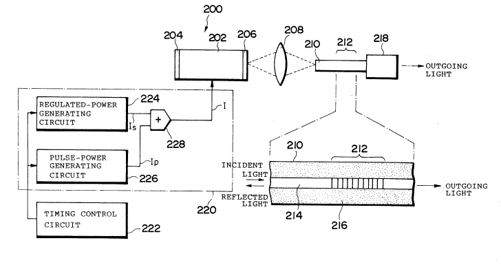
(Embodiment 1)
Fig. 1 is a schematic view showing a configuration
of an OTDR apparatus 100 in this embodiment. This OTDR
apparatus 100 is constituted by an inspection light
source 110, an optical coupler 40, and a measurement
section 50.
The inspection light source 110 oscillates in a
pulsing manner to emit laser light. It is constituted
by a Fabry-Perot type semiconductor laser 10, a lens
20, and an optical fiber 30. It is formed as the
optical fiber 30 is optically connected, by way of the
lens 20, to the Fabry-Perot type semiconductor laser 10
which has been conventionally used as inspection light
source of an OTDR apparatus. This inspection light
source 110 is similar to that disclosed in a paper of
D.M. Bird et al (Electron. Lett., Vol. 30 , No. 13, pp.
- . ~1865gS
SEI 96-22
1115-1116, 1994).
The Fabry-Perot type semiconductor laser 10 is a
semiconductor light-emitting device constituted by a
hetero-structure of InGaAsP/InP. When an operating
current flows therethrough, it is excited so as to
output pulse light of 1,550 nm band. On both sides of
the hetero-structure, a light-reflecting surface 11 and
a light-emitting surface 12 are respectively disposed.
These surfaces are opposed to each other, thereby
forming a Fabry-Perot laser resonator. The light-
reflecting surface 11 has a high reflectance (about 80%
in this embodiment), whereas the light-emitting surface
12 has a low reflectance (about 5% i~ this embodiment).
As in the case of most Fabry-Perot type devices, the
semiconductor laser 10 is a multi-longitudinal-mode
laser and shows an oscillation spectrum in which output
increases in response to wavelengths in the respective
modes.
The lens 20 converges the light emitted from the
semiconductor laser 10 so as to make it incident on the
optical fiber 30, thereby coupling the semiconductor
laser 10 to the optical fiber 30 in terms of optical
power. As the lens 20, an ordinary optical coupling
lens such as that used in optical communications can be
employed.
Here, a tip of the optical fiber 30 may be
-- 21865q~
SEI 96-22
processed by melting or shaving to have a lens
function, thereby el;~in~ting the lens 20 which is
arranged between the semiconductor laser 10 and the
optical fiber 30.
The optical fiber 30 comprises an ordinary single-
mode optical fiber and a diffraction grating 35 formed
at a part of its core. The refractive index of this
diffraction grating 35, which is an area of the core,
periodically changes between the minimum refractive
index and the maximum refractive index according to
positions along its optical axis. The period of this
change in refractive index corresponds to the period of
the diffraction grating.
It has been known in general that, when
"interference of two lightwaves~ technique is used to
generate an interference fringe of ultraviolet rays,
and an optical fiber having a core doped with GeO, is
irradiated with thus generated interference fringe, the
diffraction grating 35 can be formed. This
manufacturing method is disclosed in Japanese
Publication of the Translation of International
Application No. 62-500052. In this method, since the
effective refractive index of the core increases
according to the optical intensity distribution of the
interference fringe, an area where the refractive index
fluctuates between the original effective refractive
54
~1865g5
SEI 96-22
index of the core and the increased effective
refractive index is formed. This area is the
diffraction grating 35.
The diffraction grating 35 reflects light over a
narrow wavelength width whose center is a predetermined
reflection wavelength A~. This reflection wavelength A~
is expressed as:
A~ = 2 ~ n A (1)
wherein n is the effective refractive index of the
diffraction grating 35 and A is the period of the
diffraction grating 35.
The optical coupler 40 is a kind of an optical
- directional coupler having four termin~ls~ i.e., first
to third t~rm;n~ls 41 to 43 and a resistive term;n~tor
44. The first terminal 41 is connected to the optical
fiber 30 such that the inspection light from the
inspection light source 100 is incident on the optical
coupler 40. To the second terminal 42, an optical
fiber 60 to be measured is connected.
The inspection light incident on the optical
coupler 40 is split into two light components. One of
the split light components is made incident on the
optical fiber 60 to be measured. Of the incident
inspection light, backscattering light which has been
made to advance in the opposite direction due to
Rayleigh scattering at each point of the optical fiber
21865~S
SEI 96-22
60 is made incident on the optical coupler 40 and then
split into two. One of thus split light component is
made incident on the measurement section 50.
As in the case of the conventional OTDR apparatus,
an optical directional coupler such as optical
circulator may be used in place of the optical coupler
40.
The measurement section 50, which measures the
backscattering light of the optical fiber 60 to be
measured, is connected to the third terminal 43 of the
optical coupler 40. The measurement section 50, which
is similar to that used in ordinary OTDR apparatuses,
comprises a photodetector which detects the
backscattering light and converts thus detected light
into an electric signal; an amplifier for amplifying
the electric signal output from the photodetector; a
signal processing section which A/D-converts the signal
output from the amplifier and further subjects thus
converted signal to an averaging processing or the
like; a CRT device connected to the signal processing
section; and the like. Based on the output signal of
the signal processing section, the CRT device displays
the scattering light power of the optical fiber 60 with
respect to the distance from a predetermined reference
point to the measurement point in the optical fiber 60.
As thus displayed waveform is observed, loss between
21865 IS
SEI 96-22
two arbitrary points in the optical fiber can be
determined.
The inspection light source 110 outputs laser
pulse light having a wavelength width narrower than the
output wavelength width of the semiconductor laser 10.
The principle thereof will be explained in the
following.
When an operating current flows through the Fabry-
Perot type semiconductor laser 10, spontaneously
emitted light is generated. As this light is
repeatedly reflected between the light-reflecting
surface 11 and the light-emitting surface 12 while
causing stimulated emission, the light is amplified so
as to finally generate laser oscillation. In this
manner, the light reflected by the light-emitting
surface 12 contributes to laser oscillation of the
semiconductor laser 10.
Nevertheless, since the reflectance of the light-
emitting surface 12 is as low as 5%, most of the
spontaneously emitted light and stimulatively emitted
light can pass through the light-emitting surface 12.
Fig. 2 is a chart showing a wavelength spectrum of
light emitted from the light-emitting surface 12. The
emitted light has a wavelength range of about 1,540 nm
to about 1,560 nm with a wavelength width of about 20
nm.
- 2186545
SEI 96-22
The light emitted through the light-emitting
surface 12 passes through the lens 20 and then is made
incident on the optical fiber 30, thereby reaching the
diffraction grating 35. Fig. 3 is a chart showing a
reflection spectrum of the diffraction grating 35. As
indicated by Fig. 3, the reflection wavelength A~ of the
diffraction grating 35 is about 1,553.3 nm, and
relatively high reflectance is exhibited over a narrow
wavelength width whose center is this wavelength.
Here, the reflectance with respect to the reflection
wavelength is about 47%.
The light reflected by the diffraction grating 35
is made incident, by way of the lens 20, on the
semiconductor laser 10 from the light-emitting surface
12, and reaches the light-reflecting surface 11 while
causing stimulated emission. The light reflected by
the light-reflecting surface 11 advances, while causing
stimulated emission, so as to be emitted from the
light-emitting surface 12 and then incident on the
optical fiber 30 again. This incident light reaches
the diffraction grating 35, where it is reflected
again. Thus, as reflection is repeated between the
diffraction grating 35 and the light-reflecting surface
11, light is amplified so as to finally generate laser
oscillation. Consequently, laser light is emitted from
the end face of the optical fiber 30 facing the optical
58
- 2~86~5
. . SEI 96-22
coupler 40. Thus emitted laser light is the inspection
laser light output from the inspection light source
110 .
The light generating laser oscillation between the
diffraction grating 35 and the light-reflecting surface
11 is limited to light having a wavelength which is
reflected by the diffraction grating 35 with a
relatively high reflectance. While the light passing
through the light-emitting surface 12 to enter the
optical fiber 30 extends over the wavelength range of
about 1,540 nm to about 1,560 nm as shown in Fig. 2,
the diffraction grating 35 reflects with a sufficient
reflectance only the light extending over a wavelength
width of about 0.3 nm whose center is about 1,553.3 nm
as shown in Fig. 3. Accordingly, light with a
wavelength width narrower than that obtained when the
semiconductor laser 10 is used alone causes laser
oscillation. Since the reflectance of the diffraction
grating 35 with respect to the reflection wavelength is
sufficiently higher than the reflectance of the light-
reflecting surface 11, the output of the laser light
due to laser oscillation between the diffraction
grating 35 and the light-reflecting surface 11 becomes
sufficiently higher than that generated by the
semiconductor laser 10. As a result, the laser light
output from the inspection light source 110 has a
21865~S
SEI 96-22
wavelength width narrower than that of the laser light
output from the semiconductor laser 10.
Fig. 4 is a chart showing an oscillation spectrum
of the inspection light source 110. As indicated by
this chart, the inspection light source 110 performs
single longitudinal mode laser oscillation. Of the
light reflected by the diffraction grating 35, only
light components exhibiting a relati~ely high
reflectance satisfy the oscillation condition.
Accordingly, the wavelength width (half-width) of the
oscillation spectrum is about 0.1 nm, which is further
narrower than the line width of the reflection spectrum
of the diffraction grating 35.
~ere, when the output wavelength width of the
inspection light source 110 is 2 nm or smaller,
characteristics of an optical fiber at a specific
wavelength can be measured preferably. The output
wavelength width of the inspection light source 110 can
be adjusted when the line width of the reflection
spectrum of the diffraction grating 35 is appropriately
set.
The inspection light source 110 of this ~mho~;ment
utilizes, as it is, a semiconductor laser which has
conventionally been used as inspection light source,
while adding the lens 20 and the optical fiber 30
thereto. Accordingly, while laser oscillation occurs
- ~186S~
SEI 96-22
between the diffraction grating 35 and the light-
reflecting surface 11, laser oscillation also occurs in
the semiconductor laser 10 between the light-reflecting
surface 11 and the light-emitting surface 12.
Nevertheless, since laser-light with a narrow
wavelength width can be obtained when laser oscillation
is generated between the diffraction grating 35 and the
light-reflecting surface 11, laser oscillation in the
semiconductor laser 10 is not always necessary in
practice. Accordingly, the reflectance of the light-
emitting surface 12 can be made lower than that in this
embo~;ment without the reflectance o~ the light-
reflecting surface 11 being changed. Since the power
of the light emitted from the light-emitting surface 12
is enhanced in this manner, the reflectance of the
diffraction grating 35 may be made lower than that in
this ~mho~;m~nt.
Since the OTDR apparatus 100 of this embodiment
comprises the above-mentioned inspection light source
110 and thereby uses laser light with a sufficiently
narrow wavelength width as inspection light,
characteristics of the optical fiber 60 to be measured
at a specific wavelength can be preferably measured.
Also, the inspection light source 110 has a simple
configuration constituted by the semiconductor laser
10, the optical fiber 30, and the lens 20 for optically
~1865q~
SEI 96-22
coupling them together. Thus, the number of parts in
the OTDR apparatus 100 is remarkably smaller than that
in the conventional OTD~ apparatus using an optical
fiber laser as its light source. Accordingly, the OTDR
apparatus 100 of this embodiment is advantageous in
that designing of optical systems and disposition of
optical parts therein are easy, and that the apparatus
can be made effortlessly with a smaller size. The
small number of parts and the effortless manufacture
lead to a low manufacturing cost. Accordingly, the
OTDR apparatus of this embodiment is also suitable for
mass production.
(Embodiment 2)
The OTDR apparatus of this embodiment differs from
that of Embodiment 1 in that it comprises an inspection
light source which, in addition to the constituents of
the inspection light source 110 in Embodiment 1,
further comprises a stress applying device 70 for
applying a stress to the optical fiber 30.
Fig. 5 is a view showing a configuration of the
stress applying device 70. The stress applying device
70 comprises arms 71 and 72 for holding the optical
fiber 30 respectively at two points between which the
diffraction grating 35 is held, and a piezoelectric
device 73 to which the arms 71 and 72 are attached. To
the piezoelectric device 73, a non-depicted variable
-- 21865~5
SEI 96-22
voltage source is connected. The piezoelectric device
73 expands or contracts as a driving voltage is applied
thereto from the variable voltage source. The
direction of expAnsion or contraction is substantially
in parallel to the optical-axis direction of the
optical fiber 30.
When the piezoelectric device 73 ~p~n~ or
contracts, a stress (tension or pressure) is applied,
by way of the arms 71 and 72, to the optical fiber 30
in the optical-axis direction. Consequently, the
period of the diffraction grating 35 or the effective
refractive index of the core changes. Since the
reflection wavelength of the diffraction grating 35
depends on the period of the diffraction grating 35 and
the effective refractive index of the core as indicated
by the above-mentioned expression (1), the reflection
wavelength of the diffraction grating 35 also changes
in response to their changes. When the reflection
wavelength changes, the output wavelength of the
inspection light source also changes. Accordingly,
when the magnitude or polarity of the driving voltage
for the piezoelectric device 73 is adjusted so as to
control the expansion and contraction of the
piezoelectric device 73, the output wavelength of the
inspection light source can be arbitrarily switched
over. In this embodiment, an output wavelength change
2186595
SEI 96-22
of 10 nm/kg can be realized.
Thus, since the OTDR apparatus of this embodiment
comprises an inspection light source with a variable
wavelength, it can select a wavelength from a
predetermined variable wavelength range so as to
measure characteristics of the optical fiber to be
measured at this wavelength. While this inspection
light source attaches the stress applying device 70 to
the optical fiber 30 of the inspection light source 110
in Embs~;mcnt 1, no new optical parts are added
thereto. Accordingly, as in the case of Embodiment 1,
the OTDR apparatus of this embodiment is also
advantageous in that designing of optical systems and
disposition of optical parts therein are easy, and that
the apparatus can be made effortlessly. Also, even
though the stress applying device 70 is added thereto,
the number of parts is still small, and the stress
applying device 70-is a small device utilizing a
piezoelectric device. Therefore, the OTDR apparatus as
a whole can attain a sufficiently small size.
(Embodiment 3)
In the OTDR apparatus of this embodiment, the
configuration of the inspection light source also
differs from the inspection light source 110 of
Embodiment 1. Namely, the inspection light source in
the OTDR apparatus of this embodiment further
64
21865q~
SEI 96-22
comprises, in addition to the constituents of the
inspection light source 110 in Embodiment 1, a
temperature adjusting bath storaging the part of the
optical fiber 30 including the diffraction grating 35.
This temperature adjusting bath arbitrarily changes the
temperature therein within a predetermined temperature
range.
Also, in this emhoA;~e~t, as shown in Fig. 6, the
optical fiber 30 is buried in a V-shaped groove 91 of a
stationary plate 90. To the part of the optical fiber
30 including the diffraction grating 35, a metal plate
(aluminum plate) 80 is attached. This aluminum plate
80 is bonded by means of an adhesive to the optical
fiber 30 at two positions between which the diffraction
grating 35 is held.
When the temperature within the temperature
adjusting bath is changed, a stress is applied to the
optical fiber 30 in response to the difference between
the coefficient of thermal exp~n~ion of the aluminum
plate 80 and that of the optical fiber 30.
Consequently, the part of the optical fiber 30
including the diffraction grating 35 expands or
contracts along the optical-axis direction, whereby the
period of the diffraction grating 35 changes to shift
the reflection wavelength. Accordingly, when the
temperature within the temperature adjusting bath is
2186~4S
SEI 96-22
regulated, the output wavelength of the inspection
light source can be arbitrarily switched over. In this
embodiment, an output wavelength change of 0.05 nm/ C
can be realized.
Here, since the optical fiber 30 itself e~p~n~ or
contracts when the temperature within the temperature
adjusting bath changes, the reflection wavelength of
the diffraction grating 35 can change even when the
aluminum plate 80 is not provided. When the aluminum
plate 80 is provided, however, the change in reflection
wavelength with respect to change in temperature
increases, whereby the output wavelength of the
inspection light source can be advantageously switched
over within a broader wavelength range. Also, better
controllability is attained when the aluminum plate 80
is provided.
Since the OTDR apparatus in this embodiment also
comprises a wavelength-variable inspection light source
as in the case of the OTDR apparatus in Embodiment 2,
it can select a wavelength from a predetermined
variable wavelength range so as to measure
characteristics of the optical fiber to be measured at
this wavelength. Also, this inspection light source
adds no new optical parts to the configuration of the
inspection light in Embodiment l and, accordingly, is
advantageous in that designing of optical systems and
66
- 2186S~5
SEI 96-22
disposition of optical parts therein are easy, and that
the apparatus can be made effortlessly.
(Embodiment 4)
First, a pulse laser light source used in the OTDR
apparatus of this embodiment will be explained.
With reference to Figs. 7 to 11, a first example
of the pulse laser light source will be explained.
Initially, with reference to Fig. 7, provided in the
apparatus is a semiconductor light-emitting device
(Fabry-Perot type laser) 200 comprising a laser medium
202 made of a semiconductor having a hetero-structure
of InGaAsP/InP, for example, and light-reflecting
surfaces 204 and 206 which are opposed to each other
and respectively disposed at both ends of the laser
medium 202. One light-reflecting surface 204 has a
high reflectance of about 80%, for example, while the
other light-reflecting surface 206 has a low
reflectance of about 5%, for example, such that the
laser light stimulatively emitted at the laser medium
202 passes through and exits from the light-reflecting
surface 206.
A condenser lens 208 is disposed so as to face the
light-reflecting surface 206. Disposed to face the
condenser lens 208 from behind is an end face of a core
in an optical fiber 210 in which an optical waveguide
type diffraction grating 212, which will be explained
67
'- 2186545
SEI 96-22
later, is formed. ~ere, both the position from which
the laser light exits and the end face of the core in
the optical fiber 210 are disposed so as to coincide
with the optical axis of the condenser lens 208.
As shown in a longitudinal cross section depicted
as being enlarged in Fig. 7, the optical waveguide type
diffraction grating 212 has such a configuration that,
as ultraviolet rays or the like have irradiated a part
of a core 214 disposed in a clad 216 of the optical
fiber 212 along the optical wave-guiding direction
thereof, a plurality of refractive-index changing
portions (depicted as banded portions) having
refractive index n2 which is different from original
refractive index nl of the core 212 (n2< nl in this
embo~;ment) are formed. Namely, it has a so-called
refractive-index change distribution in which portions
with refractive indices n~ and n, periodically alternate
with a predeter~;ned pitch ~ along the optical wave-
guiding direction, and exhibits a wavelength
selectivity for selectively reflecting, of the light
transmitted through this refractive-index change
distribution, wavelength light with A = 2nl~. Namely,
when incident light is introduced into the core212
from one end (side facing the condenser lens 208), the
light with the wavelength A returns toward the
condenser lens 208 as reflected light due to the
68
2186~45
SEI 96-22
wavelength selectivity of the optical waveguide type
diffraction grating 212, while the light excluding the
wavelength A is output to the other end as outgoing
light. Here, the light transmittance of the optical
waveguide type diffraction grating 212 is set to about
47%.
Disposed at the other end of the optical fiber 210
is an optical connector 218 for connecting the former
to other optical fibers or the like.
Also provided are a driving section 220 for
supplying a driving current (electric power) I for
excitation to the laser medium 202, and a timing
control circuit 222 for controlling the output timing
of this driving current I. The driving section 220
comprises a stabilizing-power generating circuit 224
for outputting a stabilizing current (electric power) I.
for stabilizing laser oscillation which will be
explained later or the like, and a pulse-power
generating circuit 226 for outputting a pulse current
(electric power) Ip, while the respective output timings
of the currents I, and Ip in these circuits 224 and 226
are controlled by the timing control circuit 222.
Further provided in the driving section 220 is a
current adding circuit 228 which adds the currents I.
and Ip together so as to supply the driving current I (=
I. + Ip) to the laser medium 202.
69
2186545
SEI 96-22
In the following, the operation of the pulse laser
apparatus thus configured will be explained with
reference to Figs. 7 to 11.
The stabilizing-power generating circuit 224 in
the driving section 220 continuously outputs a certain
constant level of the stabilizing current I, under the
control of the timing control circuit 222 as shown in
Fig. 8, whereas the pulse-power generating circuit 226
outputs the pulse current Ip having a pulse form such as
that shown in Fig. 9 according to a control signal with
a predetermined timing from the timing control circuit
222.
During a period which is not designated by the
control signal from the timing control circuit 222, the
pulse current Ip is 0 A; whereas, at the time indicated
by the above-mentioned control signal, it is set to a
current level I~ which is sufficient for exciting the
laser medium 202. The stabilizing current I. is set to
a constant level of about 1/10 of the current level I~,
i.e., I~/10. Also, the stabilizing current I. is set to
a level which is at a threshold current level necessary
for the semiconductor light-emitting device 200 to
generate laser oscillation or higher. As these
currents I. and Ip are added together at the current
adding circuit 228, the driving current I (= I. + Ip)
such as that shown in Fig. 10 is supplied to the laser
-
~186545
SEI 96-22
medium 202.
During the period in which the driving current I
corresponds to the stabilizing current I, (= I~/10), the
light excited by this current I, in the laser medium 202
is introduced into the core 214 of the optical fiber
210 by way of the light-reflecting surface 206 and the
condenser lens 208, and a part of the light with the
reflection wavelength (Bragg wavelength) A set in the
optical waveguide type diffraction grating 212 is
further reflected so as to be made i~cident on the
laser medium 202 again by way of the condenser lens 208
and the light-reflecting surface 206, thereby
contributing to the stimulated emission resulting from
an interference phenomenon caused by the light-
reflecting surfaces 204 and 206. Further, thus
stimulatively emitted light is introduced into the core
214 of the optical fiber 210 by way of the light-
reflecting surface 206 and the condenser lens 208, and
a part of the light with the reflection wavelength
(Bragg wavelength) A set in the optical waveguide type
diffraction grating 212 is further reflected so as to
be made incident on the laser medium 202 again by way
of the condenser lens 208 and the light-reflecting
surface 206, thereby contributing to the above-
mentioned stimulated emission. Accordingly, as the
foregoing phenomenon of stimulated emission is
~186545
SEI 96-22
continuously generated, the Fabry-Perot type laser
emits laser light having a wavelength equal to the
reflection wavelength 1 set in the optical waveguide
type diffraction grating 212. Here, since the driving
current I during this period corresponds to the
stabilizing current I. (= I~/10), the optical intensity
of the laser light emitted during this period becomes
lower than the desired intensity of pulse laser light.
Specifically, since the relationship of I. = I./10 is
set, the former becomes lower than the latter by 10 dB.
Next, at the time in which the pulse current Ip is
generated in the driving current I, as the driving
current I rapidly increases, pulse laser light having a
pulse form with a high optical intensity is emitted
from the semiconductor light-emitting device 200 and,
by way of the condenser lens 208 and the optical fiber
210 as well as the optical connector 218, is output as
the outgoing light.
Fig. 11 schematically shows a result of
measurement in which change in the spectrum
distribution of the outgoing light output from the
optical connector 218 is actually measured with time,
with its Z axis indicating the optical intensity. ~rom
this chart, it has been confirmed that laser light at
the wavelength A with a low optical intensity is
generated during the period in which the driving
2~86S4~
SEI 96-22
current laser becomes the stabilizing current I, (=
I~/10), whereas pulse-shaped laser light at the
wavelength A with a high optical intensity is generated
at the time when the pulse current Ip is supplied. In
practice, laser light with a wavelength range having a
half-width of about 0.3 nm whose center is the
wavelength A could be realized.
Further, it is necessary for the interval between
adjacent supplies of the pulse current Ip (i.e., period
during which only the stabilizing current I, is
supplied) to be set to a period during which the light
emitted from the laser medium 202 is reflected by the
optical waveguide type diffraction grating 212 and then
returns to contribute to the stimulated emission
(period for one to-and-fro travel) or longer.
According to the result of actual measurement, when the
pulse current Ip was supplied at the time after the
- stabilizing current I, was continuously-supplied over
the period for about 200 to-and-fro travels, very
stable pulse laser light with a narrow wavelength range
could be output.
Thus, in the pulse laser light source of the first
example, before the pulse laser light with a narrow
wavelength range originally required is generated, the
stabilizing current I. is supplied to the semiconductor
light-emitting device 200 so as to effect laser
~186~4~
SEI 96-22
oscillation beforehand. Accordingly, at the time when
the pulse current Ip is supplied, pulse laser light with
a desired narrow wavelength range is obtained.
Therefore, a pulse laser apparatus whose response is
much better and whose stability concerning the narrow
wavelength range is much more preferable as compared
with those in the prior art can be provided. Namely,
in the prior art, immediately after the pulse current
is supplied to the pulse laser apparatus, light having
a wide wavelength range is generated, thereby making it
difficult to attain pulse laser light with a desired
narrow wavelength range. The pulse laser light source
of this example, by contrast, exhibits an excellent
effect that pulse laser light with a stable narrow
wavelength range can be obtained immediately after
pulse current is supplied thereto.
During the period in which only the stabilizing
current I. is supplied to the laser medium 202, laser
light, which may become a noise light component, is
also output. Nevertheless, the optical intensity of
this noise light component can be made smaller than
that of the desired pulse laser light when the
stabilizing current I, is set to a level lower than that
of the pulse current Ip as mentioned above.
Accordingly, it does not result in a substantial
problem when the pulse laser source is applied to
74
21865~5
SEI 96-22
fields of various optical instruments, optical
communications, and the like.
Here, in the driving section 220 of the pulse
laser light source in the first example, the
stabilizing-power generating circuit 224 and the pulse-
power generating circuit 226 are provided independently
from each other so as to respectively output the
stabilizing current I. and the pulse current Ip, which
are then added together in terms of current so as to
generate the driving signal I. Without being
restricted to such a configuration, however, the
present invention may be configured so as to have a
driving section which directly outputs the driving
current I having a waveform shown in Fig. 10, for
example.
In the following, the second example of the pulse
laser light source used in the OTDR apparatus of this
~embodiment will be explained with reference to Figs. 12
to 15. Here, since the configuration of this apparatus
is basically the same as the pulse laser source shown
in Fig. 7, only their differences will be explained in
detail without their overlapping explanations being
repeated.
The stabilizing-power generating circuit 224 in
Fig. 7 outputs the stabilizing current I, having a
rectangular shape as shown in Fig. 12 according to a
~18654S
SEI 96-22
control signal from the timing control circuit 222.
Further, the pulse-power generating circuit 226 outputs
the pulse current Ip having a pulse form as shown in
Fig. 13 according to a control signal output from the
timing control circuit 222. ~ere, timing control is
perfomed such that the time width (generation period)
of each rectangular block of the stabilizing current I,
is longer than that of the pulse current Ip, and that
the stabilizing current I. is synchronously output at a
time which is prior, by a predeterrined duration, to
the time at which the pulse current Ip is output.
Accordingly, the driving current I (= I, + Ip)
supplied to the laser medium 202 in Fig. 7 changes
stepwise as shown in Fig. 14. Here, during a period
which is not designated by the control signal from the
timing control circuit 222, the pulse current Ip is 0 A;
whereas, at the time indicated by the above-mentioned
control signal, it is set-to a current level I, which is
sufficient for exciting the laser medium 202. The
stabilizing current I. is set to a constant level of
about 1/10 of the current level I~, i.e., I~/10. Also,
the stabilizing current I is set to a level which is at
a threshold current level necessary for the
semiconductor light-emitting device 200 to generate
laser oscillation or higher.
When the driving current I having a waveform shown
76
~1~6S~5
SEI 96-22
in Fig. 14 is supplied to the semiconductor light-
emitting device 200 in Fig. 7, laser light with the
wavelength A set at the optical waveguide type
diffraction grating 212 is output, though with a low
optical intensity, during the time in which the
stabilizing current I, is supplied alone; whereas pulse
laser light having a high optical intensity and a
narrow wavelength range with a center wavelength of A
is output when the driving current I, in which the
pulse current Ip and the stabilizing current I. are
added together, is supplied.
Fig. 15 schematically shows a result of
measurement in which change in the spectrum
distribution of the outgoing light output from the
lS optical connector 218 is actually measured with time,
with its Z axis indicating the optical intensity. From
this chart, it has been confirmed that, though light
with a broad wavelength range is generated during a
short period of time immediately after the driving
current I rises from 0 A to I~/10 (i.e., immediately
after the stabilizing current I, rises from 0 A to
Ia/10 ); laser light at the wavelength 1 with a low
optical intensity is generated after this period has
passed, and desired pulse-shaped laser light at the
wavelength A with a high optical intensity is generated
at the time when the pulse current Ip is supplied. In
~186545
SEI 96-22
practice, laser light with a wavelength range having a
half-width of about 0.3 nm whose center is the
wavelength A could be realized.
Further, it is necessary for the interval between
adjacent supplies of the pulse current Ip (i.e., period
during which only the stabilizing current I. is
supplied) to be set to a period during which the light
emitted from the laser medium 202 is reflected by the
optical waveguide type diffraction grating 212 and then
returns to contribute to the stimulated emission
(period for one to-and-fro travel) or longer. It has
been confirmed by ~Am; n~tion that, when the pulse
current I~ is supplied at the time after the stabilizing
current I, is continuously supplied over the period for
about 200 to-and-fro travels, very stable pulse laser
light with a narrow wavelength range can be output.
Thus, according to the pulse laser light source of
the second example, though light having a broad
wavelength range is slightly generated, a pulse laser
light source whose response is much better and whose
stability concerning the narrow wavelength range is
much more preferable as compared with those in the
prior art can be provided.
During the period in which only the stabilizing
current I, is supplied to the laser medium 202, laser
light, which may become a noise light component, is
78
~186~5
SEI 96-22
also output. Nevertheless, the optical intensity of
this noise light component can be made lower than that
of the desired pulse laser light when the stabilizing
current I. is set to a level lower than that of the
pulse current Ip as mentioned above. Accordingly, it
does not result in a substantial problem when the pulse
laser source is applied to fields of various optical
instruments, optical communications, and the like.
Here, in the driving section 220 of the pulse
laser light source in the second example, the
- stabilizing-power generating circuit 224 and the pulse-
power generating circuit 226 are provided independently
from each other so as to respectively output the
stabilizing current I, and the pulse current Ip, which
are then added together in terms of current so as to
generate the driving signal I. Without being
restricted to such a configuration, however, the
present invention may be configured so as to have a
driving section which directly outputs the driving
current I having a waveform shown in Fig. 14, for
example.
In the following, a mode of realization of the
OTDR apparatus in this embodiment will be explained
with reference to Fig. 16. In Fig. 16, parts identical
or equivalent to those in Fig. 7 will be referred to
with marks identical to each other.
79
21865~
SEI 96-22
This OTDR apparatus comprises the semiconductor
light-emitting device 200 and the driving section 220
both shown in Fig. 7, as well as a t; m; ng control
circuit 230 provided in a microcomputer system or the
like. This timing control circuit 230 outputs a
control signal for making the driving section 220
supply the driving current I having a waveform such as
that shown in Fig. 10 or 14 to the semiconductor light-
emitting device 200 and also output a signal for
controlling the operation timing of the OTDR apparatus
as a whole.
The condenser lens 208 is disposed so as to face
the light-emitting end of the semiconductor light-
emitting device 200, and the core end of the optical
fiber 210 having the optical waveguide type diffraction
grating 212 is disposed so as to face the condenser
lens 208 from behind, thereby realizing the pulse laser
apparatus shown in Fig. 7.
To one side end of the optical fiber 210, a
bidirectional light-splitting coupler 234 which
optically connects to another optical fiber (referred
to as "guiding fiber" hereinafter) 232 for guiding
measurement light, which will be explained later, is
connected. Connected to the terminator of the optical
fiber 210 is an optical connector 236, to which an
optical fiber transmission line 238 or the like to be
21865~5
SEI 96-22
inspected is connected.
One end of the guiding fiber 232 is terrin~ted by
a nonreflective material or the like which inhibits
reflection of light, while the other end is connected
to a measurement section having constituents 240 to 252
explained in the following.
Namely, connected to the other end of the guiding
fiber 232 is a photodetector 240 having a photoelectric
converter device for photoelectrically converting the
measurement light guided by way of the light-splitting
coupler 234. Further connected to the photodetector
240 in cascade are an amplifier circuit 242 for
amplifying the photoelectrically-converted signal
output from the former; an AC coupled circuit 244
having an offset el;min~ting circuit for eliminating AC
components in the signal output from the amplifier
circuit 242, a low-band eli~;n~ting filter, and the
like; an A/D converter 246 for converting the signal
passed through the AC coupled circuit 244 into digital
data; an integrating and averaging circuit 248 for
integrating the digital data with a predetermined
operation period and computes the temporal mean value
thereof; a logarithmic converter circuit 250 for
logarithmically converting the temporal mean value
output from the integrating and averaging circuit 248;
and a display section 252 for displaying the
81
2186545
,
SEI 96-22
logarithmic value data output from the logarithmic
converter circuit 250 onto a CRT display or the like
through various kinds of graphic processing.
~ere, the A/D conversion timing in the A/D
converter 246 and the operation period in the
integrating and averaging circuit 248 are controlled by
the timing control circuit 230. Further, their timings
are in synchronization with the timing at which pulse
laser light with a narrow wavelength range is output
from the semiconductor light-emitting device 200
according to the driving current I.
In the following, the operation of the OTDR
apparatus in this embodiment will be explained.
As the driving current I having such a waveform as
that shown in Fig. 10 or 14 is supplied to the
semiconductor light-emitting device 200, pulse laser
light having a narrow wavelength range is emitted
therefrom and introduced into the optical-fiber
transmission line 238 by way of the optical fiber 210,
light-splitting coupler 234, and optical connector 236.
Namely, thus obtained pulse laser light hvl having a
narrow wavelength range becomes strobe light for
inspecting whether there is abnormality or the like in
the optical fiber transmission line 238 or not.
In the optical fiber transmission line 238,
backscattering light advancing toward the opposite
82
21865~5
SEI 96-22
direction (toward the optical connector 236) is
generated due to Rayleigh scattering and becomes
measurement light hV2, which is then guided to the
guiding fiber 232 by way of the light-splitting coupler
234.
Thereafter, the photodetector 240
photoelectrically converts the measurement light hV2
into a signal, which is then amplified by the amplifier
circuit 242. After unnecessary AC components are
el;min~ted therefrom by the AC coupled circuit 244,
this signal is supplied to the A/C converter 246 so as
to be converted into digital data. Further, as the
integrating and averaging circuit 248 integrates the
digital data and computes the mean value thereof, an
optical power indicative of the degree of abnormality
in the optical fiber tr~nsm;ssion line 238, distance to
the position where the abnormality is generated, or the
like is extracted. This mean value is logarithmically
converted by the logarithmic converter circuit 250, and
thus converted value is displayed on the-display
section 252, thereby indicating the result of
inspection of abnormality in the optical fiber
transmission line 238.
As this OTDR apparatus uses pulse laser light
having a very narrow wavelength range as stro~e light
hvl so as to measure an object to be measured, the
83
2186~gS
SEI 96-22
distance to the point where the abnormality occurs in
the object can be measured precisely, and measurement
with a high S/N can be perfomed.
(Embodiment 5)
Fig. 17 is a view showing a configuration of an
OTDR apparatus 10Oa in this embo~;ment. This OTDR
apparatus 100a comprises an inspection light source la
which oscillates in a pulsing manner to emit inspection
laser light for OTDR test. This inspection light
source la is formed as an optical fiber 30a is
optically connected, by way of the lens 20, to the
semiconductor light-emitting device (Fabry-Perot type
semiconductor laser) 10 which has been conventionally
used as inspection light source for OTDR apparatuses.
The Fabry-Perot type semiconductor laser 10 is a
semiconductor light-emitting device constituted by a
hetero-structure of InGaAsP/InP. To this semiconductor
laser 10, a driving circuit 13 is connected. As the
driving circuit 13 supplies an operating current
flowing through the semiconductor laser 10, the latter
is excited so as to output pulse laser light having a
wavelength range of about 20 nm extending over the
wavelength range of about 1,540 nm to about 1,560 nm.
On both sides of the hetero-structure, the light-
reflecting surface 11 and the light-emitting surface 12
are respectively disposed. These surfaces are opposed
84
~186S4~
SEI 96-22
to each other substantially in parallel, thereby
forming a Fabry-Perot type laser resonator. The light-
reflecting surface 11 has a high reflectance of about
80%, while the light-emitting surface 12 has a low
reflectance of about 5%. As in the case of most Fabry-
Perot type devices, the semiconductor laser 10 is a
multi-longitudinal-mode laser and yields large outputs
in response to wavelengths in the respective modes.
The lens 20 converges the light emitted from the
semiconductor laser 10 so as to make it incident on the
optical fiber 30a, thereby coupling the semiconductor
laser 10 to the optical fiber 30a in terms of optical
power. As the lens 20, an ordinary optical coupling
lens such as that used in optical communications can be
employed. ~ere, a tip of the optical fiber 30a may be
processed by melting or shaving to have a lens
function, thereby eliminating the lens 20 which
intervenes between the semiconductor laser lQ and the
optical fiber 30a.
The optical fiber 30a comprises an ordinary
single-mode optical fiber part and a diffraction
grating 35 formed at a predetermined part of its core.
It is disposed such that the light emitted from the
semiconductor laser 10 is incident thereon by way of
the lens 20. Though both core and clad of the optical
fiber 30a are made of quartz (SiO2) glass; the clad is
2~ 8654~
. SEI 96-22
made of substantially pure quartz glass while GeO2,
which is a material for increasing refractive index, is
added to the quartz glass constituting the core. As a
result, the core of the optical fiber 30a has a
refractive index which is higher than that of the clad
by about 0.3S%.
The diffraction grating 35 is disposed at a
position where the optical path length (with respect to
the output light of the semiconductor laser 10) from
the light-reflecting surface 11 of the semiconductor
laser 10 to the terminator (part farthest from the
semiconductor laser 10) of the diffraction grating 35
is about 70 mm. This diffraction grating 35 is an area
in the core where the effective refractive index
thereof periodically changes between the minimum
refractive index and the m~; mum refractive index
according to positions along the optical axis. In
other words, the diffraction grating 3S is an area
having an effective refractive index distribution which
repeatedly changes between the m;nimum refractive index
and the maximum refractive index along the optical
axis. ~ere, the period of this change in refractive
index is referred to as period, grating pitch, or the
like of the diffraction grating 3S.
2S As is well known, a phenomenon that, when quartz
glass doped with germanium is irradiated with
2186545
SEI 96-22
ultraviolet rays, the refractive index of thus
irradiated portion increases by an amount corresponding
to the intensity of the ultraviolet rays can be
. utilized to form the diffraction grating 35. Namely,
when an interference fringe of ultraviolet rays is
projected onto the core doped with gerr nium from the
clad surface of the optical fiber, an effective
refractive index distribution corresponding to the
optical intensity distribution of the interference
fringe is formed at the area of the core irradiated
with the interference fringe. The area having thus
formed effective refractive index distribution is the
diffraction grating 35. In this case, the m;nimllm
refractive index of the diffraction grating 35
substantially equals to the original effective
refractive index (effective refractive index before the
irradiation with ultraviolet rays) of the c~re.
The diffraction grating 35 reflects light over a
wavelength range whose center is a predetermined
2~ reflection wavelength (Bragg wavelength) AR. This
reflection wavelength 1R is expressed as:
1R = 2 ~ n ~ ~ (1)
wherein n is the effective refractive index of the
diffraction grating 35 and A is the period of the
diffraction grating 35.
The diffraction grating 35 in this embodiment is a
87
2186a~5
SEI 96-22
chirped grating in which the reflection wavelength ~
monotonously changes according to positions along the
optical axis. Since the reflection wavelength A~
changes depending on both m; n; m~l~ refractive index and
S period of the diffraction grating as indicated by the
above expression (1), the above-mentioned chirped
grating encompasses ti3 that having minimum refractive
index monotonously changing according to positions
along the optical axis and (ii) that having grating
period monotonously changing according to positions
along the optical axis. The diffraction grating 35 of
this embodiment belongs to the latter type (ii) and has
grating period which becomes greater at the position
farther from the semiconductor laser 10 along the
optical axis of the optical fiber 30a. The m;n;mum
refractive index of the diffraction grating 35 is
substantially uniform along the optical axis, while the
reflection wavelength of the diffraction grating 35 is
longer at the position farther from the semiconductor
laser 10 along the optical axis of the optical fiber
3Oa in response to the change in grating period.
Fig. 18 is a chart showing a reflection
characteristic of the diffraction grating 35 in this
embodiment. The vertical and horizontal axes in this
chart indicate reflectance and wavelength,
respectively. The peak shown in this chart is a
88
- 2186S~S
SEI 96-22
reflection spectrum of the diffraction grating 35.
This chart is obtained when a power spectrum of the
light reflected by the diffraction grating 35 is
deterr;ne~ and then the vertical axis of thus
determined spectrum is converted into the ratio of the
reflected light quantity to the incident light
quantity, i.e., reflectance. As indicated by Fig. 18,
the m~imum reflectance of the diffraction grating 35
is about 40% with respect to the reflection wavelength
of 1,550 nm, while the diffraction grating 35 has a
reflection wavelength width of about 2 nm. Here,
"reflection wavelength width of the diffraction grating
35 refers to the wavelength width between the
intersections of the line drawn in parallel to the
wavelength axis at a point which is 1/10 of the maximum
reflectance of the diffraction grating 35 and the
reflection spectrum of the diffraction grating 35 as
shown in Fig. 18.
As shown in Fig. 17, the optical coupler 40 is
connected to the inspection light source la. The
optical coupler 40 is a kind of an optical directional
coupler having four terminals, i.e., the first to third
term; n~l s 41 to 43 and the non-reflection terminal 44.
The first term; n~l 41 is connected to the optical fiber
30a such that the inspection light from the inspection
light source la is incident on the optical coupler 40.
89
21865~
SEI 96-22
To the second terminal 42, the optical fiber 60 to be
measured is connected. Accordingly, when incident on
the optical coupler 40, the inspection light from the
inspection light source la is split into two, and one
of the split light components is made incident on the
optical fiber 60 to be measured.
To the third terminal 43, the measurement section
50 is connected by way of an optical fiber 31.
Accordingly, of the inspection light incident on the
optical fiber 60 to be measured, backscattering light
which has been made to advance in the opposite
direction due to Rayleigh scattering at each point of
the optical fiber 60 is made incident on the optical
coupler 40 and split into two, and one of thus split
light components is made incident on the measurement
section 50.
As in the case of the conventional OTDR apparatus,
an optical directional coupler such as optical
circulator may be used in place of the optical coupler
40 in the OTDR apparatus of this embodiment.
The measurement section 50 measures the
backscattering light of the optical fiber 60 to be
measured. The measurement section 50, which is similar
to that used in ordinary OTDR apparatuses, comprises a
photodetector which detects the backscattering light of
the optical fiber 60 and converts thus detected light
2 1 865~
SEI 96-22
into an electric signal; an amplifier for amplifying
the electric signal output from the photodetector; a
signal processing section which converts the signal
output from the amplifier from analogue to digital and
further subjects thus converted signal to an
integrating and averaging processing, logarithmic
conversion, or the like; a display device connected to
the signal processing section; and the like. ~ere, the
A/D conversion or integrating and averaging perfomed by
the signal processing section is effected while the
light emission timing of the semiconductor laser 10 is
controlled by way of the driving circuit 13. Based on
the output signal of the signal processing section, the
display device displays the scattering light power of
the optical fiber 60 with respect to the distance from
a predetermined reference point to the measurement
point in the optical fiber 60. As thus displayed
wavefor~ is observed, loss between two arbitrary points
in the optical fiber 60 can be determined. Also, based
on thus determined loss value, fusion-spliced points in
the optical fiber 60 can be identified, for example.
In the following, the principle of light emission
in the inspection light source la will be explained.
When the driving circuit 13 supplies an operating
current flowing through the Fabry-Perot type
semiconductor laser 10, spontaneously emitted light is
91
21~65~S
SEI 96-22
generated within the hetero-structure in the
semiconductor laser 10. As this light is repeatedly
reflected between the light-reflecting surface 11 and
the light-emitting surface 12 while causing stimulated
emission, the light is amplified so as to finally
generate laser oscillation. In this manner, the light
reflected by the light-emitting surface 12 contributes
to laser oscillation of the semiconductor laser 10.
Nevertheless, since the rèflectance of the light-
emitting surface 12 is as low as 5%, most of the
spontaneously emitted light and st;~-71~tively emitted
light can pass through the light-emitting surface 12.
While being converged by the lens 20, the light
transmitted through the light-emitting surface 12 is
made incident on the optical fiber 30a and reaches the
diffraction grating 35. As indicated by Fig. 18, the
diffraction grating 35 reflects light over a reflection
wavelength width of about 2 nm whose center is the
reflection wavelength width AR. The light reflected by
the diffraction grating 35 passes through the lens 20
and then is made incident, by way of the lens 20, on
the semiconductor laser 10 from the light-emitting
surface 12, and reaches the light-reflecting surface 11
while causing stimulated emission. The light reflected
by the light-reflecting surface 11 advances, while
causing stimulated emission, so as to be emitted from
92
2186~5
SEI 96-22
the light-emitting surface 12 and then incident on the
optical fiber 3Oa again. This incident light reaches
the diffraction grating 35, where it is reflected
again. Thus, as reflection is repeated between the
diffraction grating 35 and the light-emitting surface
11, light is amplified so as to finally generate laser
oscillation. Thus generated laser light passes through
the diffraction grating 35 and is emitted from the end
face of the optical fiber 30a facing the optical
coupler 40. Thus emitted laser light is inspection
laser light output from the inspection light source la.
Fig. 19 is a chart showing a characteristic of
inspection light output from the inspection light
source la. The vertical and horizontal axes in this
chart respectively indicate power of inspection light
and wavelength. Also, the peak shown in this chart is
a power spectrum of the inspection light. The light
generating the laser oscillation between the
diffraction grating 35 and the light-reflecting surface
11 is substantially restricted to, of the light emitted
from the semiconductor laser 10, the light component
included in the reflection wavelength range of the
diffraction grating 35. In this embodiment, since the
reflection wavelength width of the diffraction grating
35 is about 2 nm, the wavelength width of inspection
light is also about 2 nm. Here, ~wavelength width of
21~6~
SEI 96-22
inspection light" refers to the wavelength width
between the intersections of the line drawn in parallel
to the wavelength axis at a point where the power is
lower than the maximum power of the inspection light by
20 dB and the power spectrum of the inspection light as
shown in Fig. 19.
When the wavelength width of the inspection light
used for an OTDR test is too small, time-coherency of
the inspection light becomes so high that specific
noise such as fading noise increases, thereby making it
difficult to perfom the OTDR test with a high accuracy.
According to experiments effected by the inventors, the
noise level in OTDR tests becomes 0.lS dB or lower when
the wavelength width of the inspection light is about 1
nm or greater. Since the loss at a point to which the
optical connector is connected in the optical fiber is
about 0.20 dB, when the noise level is 0.15 dB or
lower, the connecting point of the optical conector and-
a noise can be distinguished from each other so as to
identify the connecting point of the optical connector.
Accordingly, this level is considered to be practical
for OTDR apparatuses.
As explained in the foregoing, in the OTDR
apparatus in this embodiment, since the reflection
wavelength width of the diffraction grating 35 is
broader than 1 nm, the wavelength width of the
94
~1~6~
SEI 96-22
inspection light is also broader tha~ 1 nm. As the
time-coherency of the inspection light is sufficiently
lowered thereby, OTDR tests with a high accuracy can be
perfomed while fading noise is sufficiently suppressed.
Actually, when the inventors perfomed an OTDR test by
using the OTDR apparatus lOOa of this emho~;m~nt, noise
level was about 0.05 dB, and preferable results were
obtained.
Also, in the OTDR apparatus lOOa of this
embodiment, since the reflection wavelength width of
the diffraction grating 35 is narrower than 20 nm,
which is the output wavelength width of the
semiconductor laser 10, the wavelength width of
inspection light is also narrower than the output
wavelength width of the semiconductor laser 10.
Accordingly, in the OTDR apparatus lOOa of this
embodiment, characteristics of the optical fiber 60 to
be measured at a specific characteristic can be
measured preferably.
Further, since the diffraction grating 35 in the
OTDR apparatus lOOa of this embodiment is a chirped
grating having a reflection wavelength width
corresponding to the width of change in grating period.
Accordingly, the reflection wavelength width of the
diffraction grating 35 can be easily adjusted at the
time when it is manufactured. The wavelength width of
2186S45
-
SEI 96-22
the inspection light output from the inspection light
source la is determ;ned according to the reflection
wavelength width of the diffraction grating 35.
Accordingly, the OTDR apparatus 100a of this embodiment
can be easily made to output inspection light having a
desired wavelength width.
Also, in the OTDR apparatus 100a of this
embo~;ment, the diffraction grating 35 is disposed such
that a part thereof on the short reflection wavelength
side, i.e., the part with a smaller grating period, is
directed toward the semiconductor laser 10.
Accordingly, light from the semiconductor laser 10
advances from the part of the diffraction grating 35 on
the short reflection wavelength side toward the long
reflection wavelength side. This disposition is
effected in view of the following phenomenon. As
disclosed in a paper by g.O. Hill et al., "Application
- of Phase Masks to the Photolithographic Fabrication of
Bragg Gratings in Conventional Fiber/Planar Waveguides
with Enhanced Photosensitivity~ (OFC PD, 15-1, 1993),
the diffraction grating has a characteristic of
outwardly emitting, at each part thereof, light having
a wavelength shorter than the reflection wavelength at
that part. Accordingly, when the diffraction grating
35, which is a chirped grating, is disposed such that
the part thereof on the long reflection wavelength side
- - ~186a~S
.
SEI 96-22
is directed toward the semiconductor 10, the light
which should be reflected at the part on the short
reflection wavelength side is partially emitted outward
at the time when it passes through the long reflection
wavelength side, whereby, in the light reflected by the
diffraction grating 35, the component on the short
wavelength side becomes less than that on the
longitudinal wavelength side. As a result, in the
power spectrum of inspection light, the power on the
short wavelength side becomes lower than that on the
long wavelength side, whereby the inspection light does
not have a uniform power over the wavelength range
thereof.
In the OTDR apparatus lOOa of this embodiment,
since the diffraction grating 35 is disposed such that
the part on the short reflection wavelength side is
directed toward the semiconductor laser 10, such a
phenomenon that the light which should be reflected at
each part of the diffraction grating is emitted outward
before being reflected can be prevented. As a result,
the inspection light has a substantially uniform power
over the whole wavelength range. Accordingly, the OTDR
apparatus lOOa of this embodiment can quite preferably
perfom OTDR tests of the optical fiber 60 to be
measured.
When the wavelength of the light reflected by the
97
21865~15
SEI 96-22
diffraction grating 35 has a significant width, it is
preferable that the long-wavelength reflection side be
disposed farther from the semiconductor laser 10 than
is the short-wavelength reflection side, and that the
wavelength distribution of reflectance in the
diffraction grating 35 be set as explained in the
following.
When the pulse width of inspection light is
relatively long, the diffraction grating 35 is
preferably disposed such that reflectance of the
diffraction grating monotonously increases along the
direction moving away from the semiconductor light-
emitting device 10.
The wavelength light reflected at a position of
the diffraction grating 35 farther from the
semiconductor laser 10 has a longer resonator length,
thereby having a more attenuated optical power.
Accordingly, when the diffraction grating is disposed
such that the reflectance thereof monotonously
increases along the direction moving away from the
semiconductor light-emitting device, the power of
reflected light can be made substantially uniform
regardless of the point of reflection. Therefore,
inspection light having a substantially uniform power
over the whole area of reflection wavelength can be
used, whereby OTDR tests can be perfomed preferably.
98
~186~a
--
SEI 96-22
When the pulse width of inspection light is short,
by contrast, the diffraction grating 35 is preferably
disposed such that reflectance of the diffraction
grating monotonously decreases along the direction
moving away from the semiconductor light-emitting
device 10.
When the pulse width is shortened, there is a case
where an effect that in3ection energy can be made
smaller on the long wavelength side surpasses the
influence of the resonator length. In such a case,
when reflectance is made to decrease as the resonator
length is longer, inspection light with a substantially
uniform power over the whole reflection wavelength
range can be output.
(Embs~;me~t 6)
Fig. 20 is a view showing a configuration of an
OTDR apparatus lOOb in this embo~iment. The OTDR
apparatus lOOb of this embodiment differs from that of
Embodiment 1 in the configuration of an optical fiber
30b optically connected to the semiconductor laser 10
in an inspection light source lb. Namely, in this
embodiment, two diffraction gratings 36 and 37 are
provided in a core of the optical fiber 30b.
The diffraction grating 37 is disposed at a
position where the optical path length (with respect to
the output light of the semiconductor laser 10) from
21~65~5
SEI 96-22
the light-reflecting surface 11 of the semiconductor
laser 10 to the terminator (part farthest from the
semiconductor laser 10) of the diffraction grating 37
is about 70 mm. The diffraction grating 36 is disposed
at a position closer to the semiconductor laser 10 than
is the diffraction grating 37.
Each of the diffraction gratings 36 and 37 is a
diffraction grating with a constant pitch, in which a
predetermined grating period is maintained along the
optical axis. The diffraction grating 36 has a period
smaller than that of the diffraction grating 37, while
their minimum refractive indices nearly equal to each
other. Consequently, the diffraction grating 36 has a
reflection wavelength smaller than that of the
diffraction grating 37. Specifically, the reflection
wavelength of the diffraction grating 36 is about 1,550
nm, whereas that of the diffraction grating 37 is about
1,554 nm. The reflection wavelength-width-of each
diffraction grating is about 1 nm. ~ere, "reflection
wavelength width of the diffraction grating" is defined
as explained for Embodiment 5.
The area composed of the diffraction gratings 36
and 37 can be regarded as a single reflecting area 38
which reflects light over a predetermined wavelength
range. Fig. 21 is a chart showing a reflection
characteristic of this reflecting area, where a
100
~1865qS
SEI 96-22
reflection spectrum made of two peaks corresponding to
the respective diffraction gratings is exhibited. The
reflection wavelength width of this reflecting area 38
is about 5 nm. Here, "reflection wavelength width of
S the reflecting area 38" refers to, among the
intersections between the line drawn in parallel to the
wavelength axis at a point which is 1/10 of the maximum
reflectance of the reflecting area 38 and the
reflection spectrum of the reflecting area 38, the
wavelength width between the point at which the
wavelength is maximized and the point at which the
wavelength is minimized as shown in Fig. 21.
In this ~mho~; ment, of the light emitted from the
semiconductor laser 10, the light component repeatedly
reflected between the light-reflecting surface 11 of
the semiconductor laser 10 and the reflecting area 38
is subjected to laser oscillation and then output from
the inspection light source lb as inspection light.
Fig. 22 is a chart showing a characteristic of this
inspection light. In this embodiment, since the
reflecting area 38 composed of the diffraction gratings
36 and 37 has a reflection wavelength width of about 5
nm, the inspection light also has a reflection
wavelength width of about 5 nm. Here, "reflection
wavelength width of inspection light" refers to the
wavelength width between the intersections of the line
101
- 2186345
SEI 96-22
drawn in parallel to the wavelength axis at a point
where the power is lower than the m~X; mllm power of the
inspection light by 20 dB and the power spectrum of
inspection light as shown in Fig. 22.
Thus, in the OTDR apparatus 10Ob of this
embodiment, since the reflecting area 38 composed of
two diffraction gratings 36 and 37 having reflection
wavelengths different from each other is provided in
the optical fiber 30b, even when each diffraction
grating has a small reflection wavelength width, and
each of light components reflected by the respective
diffraction gratings and subjected to laser oscillation
has a high time-coherency, these light components are
output from the inspection light source lb as being
superposed on each other, thereby yielding a
sufficiently low time-coherency in the inspection
light. In particular, in this embodiment, since the
reflecting area 38 has a reflection wavelength width of
1 nm or greater, the wavelength width of inspection
light also becomes broader than 1 nm. Accordingly, the
time-coherency of inspection light can be securely
lowered. Therefore, OTDR tests with a high accuracy
can be securely perfomed while fading noise is
sufficiently suppressed. Actually, when the inventors
perfomed an OTDR test by using the OTDR apparatus 100b
of this embodiment, noise level was about 0.05 dB, and
102
~ 186a~5
SEI 96-22
preferable results were obtained.
Also, in the OTDR apparatus 10Ob of this
embodiment, since the reflection wavelength width of
the reflecting area 38 provided in the optical fiber
30b is narrower than 20 nm, which is the output
wavelength width of the semiconductor laser 10, the
wavelength width of inspection light is also narrower
than the output wavelength width of the semiconductor
laser 10. Accordingly, in the OTDR apparatus 100b of
this embo~ nt~ characteristics of the optical fiber
60 to be measured at a specific characteristic can be
measured preferably.
Further, in the OTDR apparatus 100b of this
embodiment, since, of the diffraction gratings 36 and
37 constituting the reflecting area 38, the diffraction
grating 36 having a shorter reflection wavelength is
disposed closer to the semiconductor.laser 10, so that
the light from the semiconductor laser 10 successively
enters the diffraction gratings from the diffraction
grating 36 having a shorter reflection wavelength. As
previously noted in explanation for Embodiment 5, a
diffraction grating has a characteristic of outwardly
emitting, at each part thereof, light having a
wavelength shorter than the reflection wavelength at
that part. Nevertheless, when the diffraction gratings
36 and 37 are disposed as in the case of this
103
- 21865~5
SEI 96-22
embodiment, such a phenomenon that the light which
should be reflected at the diffraction gratings is
emitted outward before being reflected can be
suppressed. As a result, the inspection light has a
substantially uniform power over the whole wavelength
range. Accordingly, the OTDR apparatus lOOb of this
embodiment can quite preferably perfom OTDR tests of
the optical fiber 60 to be measured.
(Embodiment 7)
Fig. 23 is a view showing a configuration of an
OTDR apparatus lOOc in this emboA;m~nt. The OTDR
apparatus lOOc of this ~mho~;ment differs from that of
Embodiment 6 in the configuration of a reflecting area
39 provided in an optical fiber 30c optically connected
to the semiconductor laser 10 in an inspection light
source lc. This reflecting area 39 is formed as the
same area of the core doped with germanium in a quartz
type single-mode optical fiber is sequentially
irradiated with ultraviolet interference fringes having
periods different from each other. The periods of the
respective interference fringes are adjusted so as to
form constant-pitch diffraction gratings having
reflection wavelengths of 1,550 nm and 1,554 nm,
respectively. Accordingly, in the reflecting area 39,
a constant-pitch diffraction grating having a
reflection wavelength of 1,550 nm and a constant-pitch
104
2186a45
i
SEI 96-22
diffraction grating having a reflection wavelength of
1,554 nm are disposed at one portion of the optical
fiber as being superposed on each other.
This reflecting area 39 exhibits a reflection
spectrum such as that obtained when the reflection
spectrum of the diffraction grating having a reflection
wavelength of 1,550 nm and the reflection spectrum of
the diffraction grating having a reflection wavelength
of 1,554 nm are superposed on each other. Thus formed
reflection spectrum is substantially the same as that
(Fig. 21) of the reflecting area 38 in the OTDR
apparatus of Embodiment 6, and the reflection
wavelength width thereof is about 5 nm. Accordingly,
the wavelength width of inspection light output from
the inspection light source lc also becomes about 5 nm.
In this embodiment, of the light emitted from the
semiconductor laser 10, the light component repeatedly
reflected between the light-reflecting surface 11 of
the semiconductor laser 10 and the reflecting area 39
is subjected to laser oscillation and then output from
the inspection light source lc as inspection light.
This inspection light has a characteristic
substantially identical to that of the inspection light
in Embodiment 6 shown in Fig. 22, and has a reflection
wavelength width of about 5 nm corresponding to the
reflection wavelength width of the reflecting area 39.
105
- 2186S~
SEI 96-22
Thus, since the OTDR apparatus 100c of this
embodiment has the reflecting area 39 composed of two
diffraction gratings having reflection wavelengths
different from each other provided i~ the same portion
of the optical fiber 30c, even when each diffraction
grating constituting the reflecting area has a small
reflection wavelength width, and each of light
components reflected by the respective diffraction
gratings and subjected to laser oscillation has a high
time-coherency, these light components are output from
the inspection light source lc as being superposed on
each other, thereby yielding a sufficiently low time-
coherency in the inspection light. In particular, in
this embodiment, since the reflecting area 39 has a
reflection wavelength width of 1 nm or greater, the
wavelength width of inspection light becomes broader
than 1 nm. Accordingly, the time-coherency of
inspection light can be.lowered securely and
sufficiently. Therefore, OTDR tests with a high
accuracy can be securely perfomed while fading noise is
sufficiently suppressed. Actually, when the inventors
perfomed an OTDR test by using the OTDR apparatus 100c
of this embodiment, noise level was about 0.05 dB, and
preferable results were obtained.
Also, in the OTDR apparatus 100c of this
embodiment, since the reflection wavelength width of
106
218~
SEI 96-22
the reflecting area 39 provided in the optical fiber
30c is narrower than 20 nm, which is the output
wavelength width of the semiconductor laser 10, the
wavelength width of inspection light is also narrower
than the output wavelength width of the semiconductor
laser 10. Accordingly, in the OTDR apparatus lOOc of
this em~odiment, characteristics of the optical fiber
60 to be measured at a specific characteristic can be
measured preferably.
(Embodiment 8)
Fig. 24 is a view showing a configuration of an
OTDR apparatus lOOd in this embodiment. The OTDR
apparatus lOOd of this ~mho~;ment differs from that of
the above-mentioned embodiment in the configuration of
an inspection light source ld. Namely, in the
inspection light source ld, the diffraction grating 36
is formed in an optical fiber 30d optically connected
to the semiconductor laser 10, while a stress applying
device 70 is further attached to a part including the
diffraction grating 36.
The diffraction grating 36 is a constant-pitch
diffraction grating maint~; n ing a predetermined grating
pitch along the optical axis. The reflection
wavelength of the diffraction grating 36 is about 1,550
nm, with a reflection wavelength width of about 1 nm.
The stress applying device 70 comprises arms 71
107
2~86~45
SEI 96-22
and 72 which hold the optical fiber 30d respectively at
two points between which the diffraction grating 36 is
held, and a piezoelectric device 73 having both ends
respectively attached to the arms 71 and 72. Connected
to the piezoelectric device 73 is a non-depicted
variable voltage source, from which a driving voltage
is applied to the piezoelectric device 73 so as to make
the latter ~p~n~ or contract. ~ere, the directions of
expAnsion and contraction are substantially in parallel
to the optical-axis direction of the optical fiber 30d.
When the piezoelectric device 73 expands or
contracts, a stress (tension or pressure) is applied to
the optical fiber 30d along the optical-axis direction
by way of the arms 71 and 72. As a result, the period
or m;n;mum refractive index of the diffraction grating
36 changes. As indicated by the above-mentioned
expression (1), the reflection wavelength of the
diffraction grating 36 depends on the period and
minimum refractive index of the diffraction grating 36.
Accordingly, the reflection wavelength of the
diffraction grating changes in response to the change
in the period and minimum refractive index thereof.
According to experiments effected by the inventors, the
reflection wavelength of the diffraction grating 36 can
be increased by about 1 nm when a tension of 100 g is
applied thereto.
- 108
~186545
SEI 96-22
In this embodiment, of the light emitted from the
semiconductor laser 10, the light component repeatedly
reflected between the light-reflecting surface 11 of
the semiconductor laser 10 and the diffraction grating
36 is subjected to laser oscillation and then output
from the inspection light source ld as inspection
light. Since the wavelength range of the inspection
light is deterri n~ according to the reflection
wavelength range of the diffraction grating 36, the
wavelength range of the inspection light changes when
the reflection wavelength of the diffraction grating 36
changes. Accordingly, when the driving voltage of the
piezoelectric device 73 is adjusted so as to control
the expansion and contraction of the piezoelectric
device 73, the wavelength range of the inspection light
can be arbitrarily regulated.
Actually, as shown in the reflection
characteristic chart of Fig. 25, when the stress
applying apparatus 70 shifts the reflection wavelength
of the diffraction grating 36 by about 4 nm, thereby
shifting the reflection wavelength range by a
wavelength width of about 5 nm; the m~X; mum power of
the inspection light also shifts by about 4 nm as shown
in the inspection light characteristic chart of Fig.
26. Accordingly, when the driving voltage level is
periodically changed with time so as to periodically
109
218fi~4~
SEI 96-22
change the reflection wavelength range of the
diffraction grating 36 with time with a wavelength
width of about 5 nm, the wavelength range of the
inspection light also periodically changes with a
wavelength width of about 5 nm. In this case, the
inspection light source ld is equivalent to a light
source having a wavelength width of about S nm. ~ere,
"changing the reflection wavelength range of the
diffraction grating 36 with time with a wavelength
width of about 5 nmn refers to a case where the
reflection wavelength range is changed with time such
that, in a reflection characteristic chart of the
diffraction grating 36, when an intersection between a
line drawn in parallel to the wavelength axis at a
point which is 1/10 of the m~;ml~m reflectance of the
diffraction grating 36 and the reflection spectrum of
the diffraction grating 36 is determined per time, the
wavelength width between the point at which the
wavelength is minimized and the point at which the
wavelength is maximized becomes about 5 nm. Also,
"wavelength range of the inspection light periodically
changes with time with a wavelength width of about 5
nm" refers to a case where the wavelength range changes
with time such that, in a characteristic chart of the
inspection light, when an intersection between a line
drawn in parallel to the wavelength axis at a point
110
21865~
SEI 96-22
where power is lower than the m~x;mllm power of the
inspection light by 20 dB and the power spectrum of the
inspection light is determined per time, the wavelength
width between the point at which the wavelength is
S m;n;m; zed and the point at which the wavelength is
m~;m; ~ed becomes about 5 nm.
Thus, in the OTDR apparatus lOOd of this
embodiment, as the reflection wavelength range of the
diffraction grating 36 is changed with time by the
stress applying apparatus 70, the wavelength range of
inspection light can be changed with time, whereby
inspection light having a substantially broad
wavelength width and a sufficiently low time-coherency
can be obtained. Accordingly, in the OTDR apparatus
lOOd of this PmhoA;ment, OTDR tests with a high
accuracy can be securely perfomed while fading noise is
sufficiently suppressed. Actually, when the inventors
perfomed an OTDR test by using the OTDR apparatus lOOd
of this embo~ime~t~ noise level was about 0.05 dB, and
preferable results were obtained.
Also, in the OTDR apparatus lOOd of this
embodiment, since the substantial reflection wavelength
width of the diffraction grating 36 is narrower than 20
nm, which is the output wavelength width of the
semiconductor laser 10, the substantial wavelength
width o~ inspection light is also narrower than the
111
~186545
SEI 96-22
output wavelength width of the semiconductor laser 10.
Accordingly, in the OTDR apparatus lOOd of this
embodiment, characteristics of the optical fiber 60 to
be measured at a specific characteristic can be
measured preferably.
Though the stress applying device 70 is used to
apply a stress to the diffraction grating 36 so as to
change the reflection wavelength range of the latter in
this embodiment, the part of the optical fiber 30d
including the diffraction grating 36 may be
accommodated in a temperature adjusing bath instead,
and the temperature within the bath may be changed.
When the temperature around the diffraction grating 36
changes, the diffraction grating 36 ~xpAn~ or
contracts along the optical-axis direction, thereby
changing the reflection wavelength of the diffraction
grating 36. Accordingly, when the temperature within
the temperature adjusting bath is regulated, the
wavelength range of inspection light can be adjusted.
In this case, when a member (e.g., plate made of a
metal such as aluminum) having a coefficient of thermal
ion different from that of the optical fiber 30d
is attached to the part of the optical fiber 3Od
including the diffraction grating 36, the change in
reflection wavelength of the diffraction grating due to
the change in temperature preferably increases.
112
2186~4~
SEI 96-22
According to experiments effected by the inventors,
when the aluminum plate is attached thereto, the
reflection wavelength of the diffraction grating 36 can
be increased by 2 nm as the temperature within the
temperature adjusting bath is raised by 10 C.
Figs. 27 and 28 are configurational views
respectively showing modified examples of the OTDR
apparatus in accordance with the above-mentioned
Em~odiment 1. Fig. 27 shows an OTDR apparatus in which
an optical isolator 91 and a tr~nsm;ssion type band
pass filter 92 are inserted between the inspection
light source 110 and the optical coupler 40. Fig. 28
shows an OTDR apparatus in which an optical circulator
30a is adopted, and a reflection type band pass filter
93 is inserted in an optical path between the
inspection light source 110 and the optical fiber 60 to
be measured.
- ~ In the embo~i~~nts where one of facing mirrors of
the inspection light source 110 is constituted by the
diffraction grating 35 formed in the optical waveguide
30, the wavelength width of the oscillated laser light
is made narrower. Nevertheless, when the resonator
length becomes large, due to its relationship to pulse
width, the number of to-and-fros of light through the
resonator decreases. Accordingly, though with a low
power, oscillation wavelength cannot be prevented from
113
21865~5
SEI 96-22
expanding. When an OTDR test is perfomed, there are
cases where, in order to prevent crosstalk to a signal
transmission band from occurring, such an extension of
oscillation wavelength is desired to be reduced in an
amount beyond the capacity of the diffraction grating.
In such cases, when a band pass filter is further
provided in an optical path between the inspection
light source 110 and the optical fiber 60 to be
measured, light outside of the wavelength range
necessary for the OTDR apparatus can be cut off,
whereby a preferable output characteristic can be
obtained. As a result, influence upon optical
communications can be securely suppressed.
(Embodiment of Optical cc ml~n;cation line Inspection
System)
Fig. 29 is an overall configurational view showing
an optical communication line inspection system of this
embo~;m~nt. First, a basic configuration of an optical
communication network to which the inspection system of
this embodiment is applied will be explained. One or a
plurality of optical communication lines 303
(represented by three optical communication lines in
Fig. 29) connected to a transmission apparatus 302,
which is installed in a station for a subscriber
communication network or the like, are bundled as an
optical fiber cable 304 and extend to subscribers'
114
2 1 8 6 5 ~ ~
SEI 96-22
houses 305. Accordingly, the tr~nsmission apparatus
302 and each subscriber's house 305 is connected to
each other by way of one optical communication line
303. Communication light output from the transmission
apparatus 302 is propagated through the optical
communication line 303 and received by a terminal
installed at the subscriber's house 305. In the
optical communication network of this r-~oA; ment,
signal light having a wavelength of about 1,300 nm is
used.
In the following, the configuration of the
inspection system in this embodiment will be explained.
This inspection system is constituted by an OTDR
apparatus 300; an optical switch 340 connected, by way
of an optical fiber 322, to inspection light from the
OTDR apparatus 300; an optical coupler 350 disposed at
the end portion of the optical communication line 303
on the tr~ns~ission apparatus side 302; and an optical
filter 360 disposed at the terminator portion (end
portion on the subscriber side 305) of each optical
communication line 303.
The OTDR apparatus 300 is constituted by a light-
emitting section 310; an optical coupler 320 connected
to the light-emitting section 310 by way of an optical
fiber 323; and an inspection section 330 connected to
the optical coupler 320 by way of the optical fiber
115
~ 2186a4~
SEI 96-22
323.
The light-emitting section 310 oscillates in a
pulsing manner to emit laser light which is inspection
light. The half-width of wavelength spectrum of this
inspection light, i.e., wavelength width, is about 20
nm. The center wavelength (wavelength at the center of
the half-width) is about 1,550 nm, which is different
from the wavelength of the signal light.
The optical coupler 320 makes the inspection
light, which is incident thereon by way of the optical
fiber 321, incident on the optical switch 340 by way of
the optical fiber 322; while making the returned
inspection light, which has been reflected or scattered
by each part of the optical communication line 303 and
optical filter 360, incident on the inspection section
330 by way of the optical fiber 323.
The inspection section 330 detects thus returned
inspection light so as to inspect the state of the
optical communication line 303. This inspection
section 330, which is similar to that used in ordinary
OTDR apparatuses, comprises a photodetector for
detecting the inspection light and converting thus
detected inspection light into an electric signal, an
amplifier for amplifying the electric signal output
from the photodetector, a signal processor for A/D-
converting the signal output from the amplifier and
116
- 21865~5 - -'
SEI 96-22
subjecting thus converted signal to an averaging
processing or the like; a CRT device connected to the
signal processor; and the like.
The optical switch 340 optically connects the
optical coupler 320 within the OTDR apparatus 300 and
one of the optical couplers 350 in the optical
communication line 303 to each other by way of an
optical fiber 341 in a switching manner. As the
inspection light from the OTDR apparatus 300 is made
incident on the optical communication line 303
including the connected optical coupler 350, the
optical communication line 303 to be inspected can be
selected as the optical switch 340 is operated.
The optical coupler 350 makes the inspection light
incident on the optical communication line 303 so as to
be propagated toward the subscriber's house 305; while
making the returned inspection light, which has been
reflected or scattered by each part of the optical
com~lln;cation line 303 and optical filter 360, incident
on the optical switch 340.
~ere, as can be seen from the foregoing, the
optical coupler 320, the optical switch 340, and the
optical coupler 350, as a whole, function to make the
inspection light incident on the optical communication
line 303, while making the reflected light and
backscattering light from the optical communication
117
2186a~
SEI 96-22
line 303 incident on the inspection section 330.
Namely, the optical coupler 320, the optical switch
340, and the optical coupler 350 constitute an optical
functional section exhibiting such functions.
The optical filter 360 has a function of
reflecting light over a predetermined wavelength range
so as to cut off the inspection light immediately in
front of the subscriber's house 305, thereby preventing
the inspection light from becoming noise in optical
communications. The inspection section 330 recognizes
the terminator of the optical communication line 303 by
detecting the light reflected by the optical filter
360. ~ere, in order to fully exhibit the function of
cutting off the inspection light, the optical filter
306 preferably has a reflection wavelength width
greater than the wavelength width of the inspection
light.
Fig. 30 is a chart schematically showing a
reflection spectrum of the optical filter 360 and a
wavelength spectrum of inspection light. As indicated
by this chart, the optical filter 360 preferably has a
reflection wavelength width (half-width of reflection
spectrum) broader than the wavelength width of the
inspection light.
The optical filter 360 of this embodiment is
constituted by a plurality of optical waveguide type
118
~1865~
SEI 96-22
diffraction gratings disposed in the optical
communication line 303. An optical waveguide type
diffraction grating is an area of a core of an optical
waveguide where the effective refractive index of the
core periodically changes between the minimum
refractive index and the ~X;~um refractive index along
the optical axis. This optical waveguide type
diffraction grating reflects light having a relatively
narrow wavelength width whose center is a predetermined
reflection wavelength (Bragg wavelength). It has been
known in general that the optical waveguide type
diffraction grating can be manufactured as an optical
waveguide is irradiated with an interference fringe of
ultraviolet rays, for example. Such a manufacturing
method is also disclosed in Japanese Publication of the
Translation of International Application No. 62-500052.
Though each of the plurality of optical waveguide
type diffraction gratings constituting the optical
filter 360 has a single period, the periods slightly
differ from each other among the respective optical
waveguide type diffraction gratings. Thus, when a
plurality of optical waveguide type diffraction
gratings respectively having periods slightly different
from each other are serially disposed in the optical
communication line 303 so as to constitute the optical
filter 360, the optical filter 360 exhibits a
119
2186S45
SEI 96-22
reflection spectrum with a broad wavelength width in
which reflection spectra of the respective diffraction
gratings partially overlap with each other. As the
nl~mher of the optical waveguide type diffraction
gratings is greater, the reflection wavelength width
becomes broader. An optical filter having such a
configuration is disclosed in a paper of R. Kashyap et
al., "Novel Method of Producing All Fibre Photoinduced
Chirped GratingsN (Electronics Letters, 9th June 1994,
Vol. 30, No. 12).
In order to secure a preferable function as
optical filter, a higher reflectance is more preferable
in the optical waveguide type diffraction grating.
Accordingly, an optical waveguide is exposed to a
hydrogen atmosphere and then irradiated with an
ultraviolet interference fringe so as to form an
optical waveguide type diffraction grating used in this
-emboA;m~nt. - According to this method, a~ optical
waveguide type diffraction grating having a high
reflectance can be obtained, whereby the reflectance of
the optical filter 360 can also be made high.
Nevertheless, since O~ groups generated upon
ultraviolet irradiation may absorb signal light,
thereby increasing the transmission loss; the number of
the optical waveguide type diffraction gratings
constituting the optical filter 360 is preferably as
120
2186a~S
SEI 96-22
small as possible.
Since the optical communication line 303 includes
an optical fiber which is an optical waveguide, the
optical filter 360 may be directly formed in the
optical communication line 303. Also, an optical fiber
or thin-film waveguide in which the optical filter 360
has been formed beforehand may be connected to the
optical communication line 303 so as to provide the
optical filter 360.
In the following, a method of inspecting an
optical communication line by use of the inspection
system in accordance with this embodiment will be
explained. The inspection light output from the light-
emitting section 310 is propagated through the optical
fiber 321 so as to be incident on the optical coupler
320, where it is then split into two. While one of
thus split inspection light components reaches the
resistive terminator of the aptical coupler 320, the
other is propagated through the optical fiber 322 so as
to be incident on the optical switch 340. This part of
the inspection light is made incident, by way of the
optical fiber 341 and the optical coupler 350, on the
optical communication line 303 to be measured, and then
advances through the optical communication line 303 to
reach the optical filter 360.
Due to Fresnel reflection at a fault position
121
2186a~5
SEI 96-22
(e.g., disconnected position) or Rayleigh scattering at
each point of the optical communication line 303, a
part of the inspection light returns in the direction
opposite to the advancing direction. Each of the
reflected light and backscattering light thus returned
is split into two by the optical coupler 350, and one
of thus split light components is made incident on the
optical switch 340. Thereafter, the reflected light
and backscattering light from the optical communication
line 303 is propagated through the optical fiber 322 so
as to be split into two by the optical coupler 320, and
one of thus split light components is propagated
through the optical fiber 323 so as to be incident on
the inspection section 330.
The inspection section 330 detects the reflected
light and backscattering light from the optical
communication line 303 and optical filter 360 and
subjects them to a signal processing, whereby the power
of the reflected light or backscattering light of the
optical co~mllnication line 303 is displayed on the CRT
device with respect to the distance from a
predetermined reference point to the measurement point.
As thus displayed waveform is observed, the fault
position in the optical communication line 303 as well
as loss between two arbitrary points in the optical
fiber 303 can be determined. In this manner, the
122
21865~
SEI 96-22
inspection of the optical communication line 303 is
performed.
In the optical communication line inspection
system of this embodiment, since the light-emitting
section 310 outputs light having a wavelength range as
narrow as about 20 nm or less, the reflection
wavelength width of the optical filter 360 can also be
narrowed in response thereto. Accordingly, the number
of the optical waveguide type diffraction gratings
constituting the optical filter 360 may be made small.
In particular, when the wavelength width of inspection
light is about 5 nm or less, the number of the optical
waveguide type diffraction gratings can be made very
small, whereby the optical filter 360 can be
constituted by a single optical waveguide type
diffraction grating.
When the number of the optical waveguide type
diffraction gratings is made small, the number of the
above-mentioned OH groups can be reduced as well,
whereby loss in trAns~;ssion of the signal light can be
suppressed. Also, in the case where the number of the
optical waveguide type diffraction gratings is small,
mode-mismatching occurring at the time when the signal
light passes through the diffraction gratings can be
reduced. Accordingly, trAn~ission loss can be
suppressed in this respect as well. Thus, in
123
21~65~5
SEI 96-22
accordance with the optical communication line
inspection method of this embo~;~e~t, inspection of
optical communication lines can be performed while
influence upon optical communications is sufficiently
suppressed.
As the light-emitting section 10, a variety of
configurations can be adopted. Figs. 31 to 34 are
schematic views showing configurational examples 310a
to 310d of the light-emitting section 310. In the
following, these examples will be explained with
reference to their corresponding drawings.
First, the light-emitting section 310a of Fig. 31
is constituted by a Fabry-Perot type semiconductor
laser 370, lenses 371 and 374, an isolator 372, and an
optical filter 373. Here, the optical filter 373 in
this example is a dielectric multilayer film filter.
The Fabry-Perot type semiconductor laser 370 has
an oscillation wavelength width of about 30 nm. The
lens 371 converts the laser light output from the
semiconductor laser 370 into a parallel beam and makes
this beam incident on the isolator 372. The isolator
372 has a forward direction toward the direction of
arrow in the drawing, while cutting off the light
advancing in the opposite direction. The laser light
transmitted through the isolator 372 is made incident
on the optical filter 373.
124
' ~lg654~
SEI 96-22
The optical filter 373 restricts the wavelength
width of the laser light from the semiconductor laser
370 such that, of the light included in the oscillation
wavelength range of the semiconductor laser 370, a
light component having a wavelength width of about 20
nm or less whose center is a predeterm;ned wavelength
passes therethrough. Though a part of the laser light
from the semiconductor laser 370 may be reflected by
the optical filter 373, such reflected light is cut off
by the isolator 372. Similarly, the reflected light
and scattered light from the optical communication line
are cut off. Accordingly, the light is prevented from
being incident on the resonator of the semiconductor
laser 370 and disturbing a stable oscillation state.
The laser light transmitted through the optical
filter 373 is made incident on the lens 374. While
converging the parallel beam of laser light, the lens
374 makes the laser light incident on the optical fiber
321. The laser light emitted from the lens 374 is
inspection light output from the light-emitting section
310a. As mentioned above, when the laser light from
the semiconductor laser 370 passes through the optical
filter 373, inspection light having a wavelength range
of about 20 nm or less is realized.
Next, the light-emitting section 310b of Fig. 32
is constituted by the Fabry-Perot type semiconductor
125
~186~45
SEI 96-22
laser 370, a lens 375, optical fibers 376 and 378, and
an optical circulator 377. To the optical circulator
377, the optical fibers 376 and 378 as well as the
optical fiber 321 are connected. In a part of a core
of the optical fiber 378, an optical waveguide type
diffraction grating 379 is disposed.
As in the case of the light-emitting section 310a
of Fig. 31, the semiconductor laser 370 has an
oscillation wavelength width of about 30 nm. The lens
375 converges the laser light output from the
semiconductor laser 370 and makes thus converged light
incident on the optical fiber 376, thereby connecting
the semiconductor laser 370 to the optical fiber 376 in
terms of optical power. The laser light incident on
the optical fiber 376 enters the optical circulator 377
and then is emitted to the optical fi~er 378. This
laser light advances through the optical fiber 378 and
reaches the optical waveguide type diffraction grating
379. The optical waveguide type diffraction grating
379 reflects, of the light included in the oscillation
wavelength range of the semiconductor laser 370, a
light component having a wavelength width of about 20
nm or less. This reflection light is made incident on
the optical circulator 377 and then emitted to the
optical fiber 321. The light incident on the optical
fiber 321 by way of the optical circulator 377 is
126
2186~4~
SEI 96-22
inspection light of the light-emitting section 31Ob.
Thus, since the light-emitting section 310b uses
the light reflected by the optical waveguide type
diffraction grating 379 as inspection light, when the
reflection wavelength of the diffraction grating is
about 20 nm or less, the wavelength width of inspection
light also becomes about 20 nm or less. Since it is
easy to prepare the optical waveguide type diffraction
grating having a narrow wavelength width, inspection
light having a wavelength width of S nm or less can be
easily realized in accordance with the light-emitting
section 31Ob.
Here, an optical fiber whose tip has been
processed by melting or shaving to have a lens function
may be used as the optical fiber 376, thereby
el;m;n~ting the lens 375 which intervenes between the
semiconductor laser 370 and the optical fiber 376.
Next, the light-emitting section 310c of Fig. 33
is constituted by a distribution feedback ~DFB) type
semiconductor laser 380, the lenses 371 and 374, and
the isolator 372. The laser light output from the
distribution feedback type semiconductor laser 380 is
converted into a parallel beam by the lens 371 and then
made incident on the isolator 372. The isolator 372
has a forward direction toward the direction of arrow
in the drawing, while cutting off the light advancing
127
2186~5
SEI 96-22
in the opposite direction. Accordingly, the reflected
light or backscattering light from the optical
communication line 303 is prevented from being incident
on the resonator of the semiconductor laser 380 and
disturbing a stable oscillation state. The light
transmitted through the isolator 372 is incident on the
lens 374 and then, while being converged, enters the
optical fiber 321. The laser light emitted from the
lens 374 is the output inspection light of the light-
emitting section 310c.
The wavelength width of inspection light output
from the light-emitting section 310c e~uals to the
oscillation wavelength width of the distribution
feedback type semiconductor laser 380. The
distribution feedback type semiconductor laser 380 has
a strong longitudinal-mode selectivity and a very
narrow oscillation wavelength width. Therefore, in
accordance with the light-emitting section 310c, the
wavelength width of the output inspection light can be
easily set to about 20 nm or less, and inspection light
having a wavelength width of about 5 nm or less can be
easily realized.
Finally, the light-emitting section 310d of Fig.
34 is constituted by a Fabry-Perot type semiconductor
laser 388, the lens 375, and an optical fiber 384. In
a core of the optical fiber 384, an optical waveguide
128
6 ~ 4 5 '' -
SEI 96-22
type diffraction grating 385 is formed. Also, to the
optical fiber 384, the optical fiber 321 is connected.
This light-emitting section 310d is s~ r to
that disclosed in the paper of D.M. Bird et al
(Electron. Lett., Vol. 30, No. 13, pp. 1115-1116,
1994). This light-emitting section 310d can be
regarded as a kind of distribution Bragg reflector
(DBR) type semiconductor laser.
The Fabry-Perot type semiconductor laser 388 has a
light-reflecting surface 386 with a high reflectance
and a light-emitting surface 387 with a low reflectance
respectively at both ends thereof, whereby light having
a wavelength width of about 30 nm is emitted from the
light-emitting surface 387. The lens 375 converges the
output laser light of the semiconductor laser 380 and
makes thus converged light incident on the optical
fiber 384, thereby connecting the semiconductor laser
388 to the optical fiber 384 in terms of optical power.
The light advancing through the optical fiber 384
reaches the diffraction grating 385. The diffraction
grating 385 reflects, of the light included in the
oscillation wavelength width of the semiconductor laser
388, only the light component having a wavelength width
of about 20 nm or less whose center is a predetermined
wavelength. Thus reflected light is made incident on
the semiconductor laser 388 by way of the lens 375.
129
2186a4~
SEI 96-22
The incident light advances through the semiconductor
laser 388, while causing stimulated emission, and
reaches the light-reflecting surface 386, where it is
then reflected. Thus reflected light advances through
the semiconductor 388, while causing stimulated
emission, and emitted from the light-emitting surface
387 so as to be reflected by the diffraction grating
385 again. Thus, the light is amplified as reflection
is repeated between the diffraction grating 385 and the
light-reflecting surface 386, thereby finally causing
laser oscillation. This is inspection light output
from the light-emitting section 310d. This inspection
light is transmitted through the diffraction grating
385 and made incident on the optical fiber 321.
The light causing laser oscillation between the
diffraction grating 385 and the light-reflecting
surface 386 is limited to wavelength light which is
reflected with a relatively high reflectance by the
diffraction grating 385. Accordingly, when the
diffraction grating 385 having an appropriate
reflection wavelength width is used, the wavelength
width of the output inspection light from the light-
emitting section 310d becomes about 20 nm or less.
Since the diffraction grating 385 having a narrow
reflection wavelength width can be made easily,
inspection light having a wavelength width of 5 nm or
130
21865~5
SEI 96-22
less can be easily realized in accordance with the
light-emitting section 31Od.
~ere, since the light-emitting section 31Od
outputs inspection laser light according to laser
oscillation between the diffraction grating 385 and the
light-reflecting surface 386, it is not always
necessary for the light-emitting section 310d to effect
laser oscillation at the semiconductor laser 388.
From the invention thus described, it will be
obvious that the invention may be varied in many ways.
Such variations are not to be regarded as a departure
fro~ the spirit and scope of the invention, and all
such modifications as would be obvious to one skilled
in the art are intended for inclusion within the scope .
of the following claims.
The basic Japanese Application No. 285068/1995
filed on November 1, 1995, No. 248255/1996 filed on
September 19, 1996, No. 068390/1995 filed on March 27,
1995, No. 069554/1995 filed on March 28, 1995, and No.
182867/1995 filed on July 19, 1995 are hereby
incorporated by reference.
131