Note: Descriptions are shown in the official language in which they were submitted.
2x86700
File 283
BACKC3ROUND OF THE INVENT nrr
The present invention generally relates to an automatic
implantable atrial defibrillator for delivering cardioverting
or defibrillating voltage to the atria of a patient and which
is capable of providing effective cardioversion with reduced
discomfort to the patient. The present invention is
particularly directed to such an atrial defibrillator which
includes a cardioverting output voltage limiter for simulating
output voltage waveforms provided by storage capacitors of
greater capacity than that actually delivering the
cardioverting voltage.
Atrial fibrillation is probably the most common cardiac
arrhythmia. Although it is not usually a life threatening
arrhythmia, it is associated with strokes thought to be caused
by blood clots forming in areas of stagnate blood flow as a
result of prolonged atrial fibrillation. Patients afflicted
with atrial fibrillation generally experience palpitations of
the heart and reduced cardiac output. This often leads to
dizziness or, in extreme cases, to loss of consciousness.
Atrial fibrillation is often corrected by external
defibrillation of the type well known in the art. This
treatment involves applying a relatively large quantity of
-1-
_ 2 i ~36T00
~~. File 283
electrical energy to the heart with external skin surface
electrodes. The energy is applied in synchronism with a
detected R wave (electrical activation) of the heart. The
treatment is very painful and can necessitate hospitalization
for as many as a few days. Unfortunately, most often, it only
provides temporary relief,~lasting but a few weeks.
Drugs are available for reducing the incidents of atrial
fibrillation. However, such drugs have many side effects.
Also, many patients are resistant to them which greatly
reduces their therapeutic effect.
In order to negate the need for external defibrillation
and drug therapy, implantable atrial defibrillators have been
proposed to provide relief for patients suffering from this
cardiac arrhythmia. Two such defibrillators, although
represented as being implantable, were not fully automatic,
requiring human interaction for cardioverting or
defibrillating the heart. Both of these defibrillators
required the patient to recognize the symptoms of atrial
fibrillation. One defibrillator required a visit to a
physician for activating the defibrillator. The other
defibrillator required the patient to activate ,the
defibrillator with a magnet from external to the patient's
skin.
It is preferable that an implantable cardiac device,
such as an atrial defibrillator, be truly automatic. In order
-2-
CA 02186700 2000-03-29
for an implantable atrial defibrillator to be truly automatic,
it must be able to accurately detect atrial fibrillation and
then safely apply cardioverting voltage to the atria to
convert the same to normal sinus rhythm (NSR).
Detection of atrial fibrillation is a two-part
process. First, an atrial defibrillator must be able to sense
activity of the heart, such as atrial activity. One atrial
defibrillator having such capability is fully disclosed in Jin
et al., U.S. Patent No. 5,267,559 which issued on December 7,
1993 for ATRIAL DEFIBRILLATOR AND METHOD FOR PROVIDING ATRIAL
SENSING and which is assigned to the assignee of the present
invention.
After heart activity, such as atrial activity, is
sensed, an atrial fibrillation detector then must determine if
the sensed heart activity satisfies a fibrillation criteria.
One such detector is fully disclosed in U.S. Patent No.
5,522,852 granted June 4, 1996 in the names. of Harley G. White
and Joseph M. Bocek for SELECTIVE CARDIAC ACTIVITY ANALYSIS
ATRIAL FIBRILLATION DETECTION SYSTEM AND METHOD AND ATRIAL
DEFIBRILLATOR UTILIZING SAME. Another such detector is fully
disclosed in U.S. Patent No. 5,486,199 granted January 23,
1996 in the names of Jaeho Kim and Harley G. White for SYSTEM
AND METHOD FOR REDUCING FALSE POSITIVES IN ATRIAL FIBRILLATION
DETECTION. Both of the afore-mentioned patents are assigned
to the assignee of the present invention.
- 3 -
CA 02186700 2000-03-29
Each of the aforementioned co-pending applications
discloses a preferred embodiment of an atrial fibrillation
detector wherein atrial cardiac events are detected from
sensed atrial activity. Further, each of these preferred
embodiments includes ventricular activity sensing and
detection of R waves. Atrial fibrillation is detected from
atrial activity occurring between detected R waves.
Once atrial fibrillation is detected, it is then necessary to
apply a cardioverting voltage pulse to the atria to return the
heart to NSR. To that end, a storage capacitor is charged to
a voltage and then discharged to apply the cardioverting
voltage to the heart. To assure that the cardioverting
voltage is safely applied to the atria, it is preferred that
the capacitor is discharged in synchronism with a detected R
wave. To that end, U.S. Patent No. 5,584,864 granted December
17, 1996 in the name of Harley G. White for CARDIOVERSION
SYNCHRONIZATION SYSTEM AND METHOD FOR AN ATRIAL DEFIBRILLATOR,
which is assigned to the assignee of the present invention,
discloses a synchronization system which includes two
2o ventricular sense channels and requires that an R wave be
sensed in both channels before the voltage may be applied. In
addition, other synchronization criteria may be required to be
satisfied such as a minimum interval criteria as described,
for example, in Adams et al., U.S. Patent No. 5,207,219, which
issued on May 4, 1993 for ATRIAL DEFIBRILLATOR AND METHOD FOR
- 4 -
CA 02186700 2000-03-29
PROVIDING INTERVAL TIMING PRIOR TO CARDIOVERSION, and which is
assigned to the assignee of the present invention.
Hence, as can be seen from the foregoing, an
automatic atrial defibrillator must reliably sense heart
activity, reliably detect the need for cardioversion, and
safely apply cardioverting voltage to the atria of the
patient's heart. In order to provide reasonable assurance
that the cardioverting voltage will indeed successfully
cardiovert the atria, the voltage applied should have a peak
l0 value above a determined minimum peak value required to
effectively cardiovert the atria. That voltage level is
commonly referred to as the defibrillation threshold.
The peak voltage required to effectively cardiovert
increases as the capacitor discharge time or pulse width
decreases. The capacitor discharge rate increases (resulting
in shorter capacitor discharge times) as the capacitor
capacitance decreases. Hence, larger capacitances can
discharge over a longer time period than smaller capacitances.
Also as a result, larger capacitances require a lower peak
2o voltage to effectively cardiovert.
- 5 -
~1861~0
w File 283
Since patients suffering from atrial fibrillation will
be conscious during cardioversion (unlike patients suffering
from ventricular fibrillation), perceived discomfort or pain
caused by the cardioversion becomes an issue. Obviously, the
less discomfort a patient experiences as a result of
cardioversion the better.
Discomfort or pain resulting from cardioversion is a
nervous system response to the discharged voltage. The
physiologic basis for this is that nerve tissue has a much
faster membrane time constant than cardiac muscle. Therefore_
shorter and higher peak voltage discharges create more pain or
discomfort than do longer and lower peak voltage discharges.
The logical conclusion from the foregoing would be to
use as high a capacitance as possible to cardiovert the atria.
This would result in the longest discharge time, the lowest
required peak voltage, and the least discomfort for successful
cardioversion. Unfortunately, the size of an implantable
device is also of importance. Higher capacitance values
require capacitors of larger size. Obviously, a point is
reached where capacitor size becomes impractical.
For atrial defibrillation, it has been determined that
for many patients, a capacitor having a capacitance in the
range of 70 to 100 microfarads (~F) and more particularly 80~F
with a total discharge time of six milliseconds is a suitable
choice in terms of voltage threshold and capacitor size. Some
-6-
. .".
File 283
patients, however, may experience discomfort at their voltage
threshold. For these patients, a longer discharge time and
lower voltage threshold would be more desirable.
Unfortunately, this would require a higher storage capacitance
value and hence a larger sized capacitor which may not be
practical.
The present invention provides an elegant solution to
this problem. In accordance with its broader objectives, the
present invention permits a capacitor to be discharged for a
period of time which is longer than it normally would be
discharged. It also, at the same time, permits a lower
voltage to be applied to the patient's heart to achieve
successful cardioversion. In doing so, the capacitance value,
and hence the capacitance size, need not be increased.
The present invention provides, in an implantable atrial
defibrillator which includes a storage capacitor for storing
electrical energy, switch means for discharging at least a
portion of the stored energy into a patient's heart as a
discharge voltage and charging means for charging the storage
capacitor with the stored energy to a peak voltage, the
improvement comprising limiting means for precluding the
discharge voltage from exceeding a voltage limit, the voltage
2~~6~00
File 283
limit being a substantially constant fraction of the peak
voltage.
The features of the present invention which are believed
to be novel are set forth with particularity in the appended
claims. The invention, together with further objects and
advantages thereof, may best be understood by making reference
to the following description taken in conjunction with the
accompanying drawing, in the several figures of which like
reference numerals identify identical elements, and wherein:
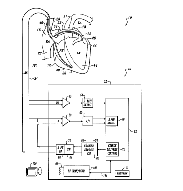
Figure 1 is a schematic block diagram of a fully
implantable atrial defibrillator embodying the present
invention for applying defibrillating voltage to the atria of
a human heart and which is shown in association with a human
heart in need of atrial fibrillation monitoring and potential
cardioversion of the atria;
Figure 2 is a schematic diagram of a preferred
embodiment of the present invention; and
Figure 3 illustrates superposed voltage versus time
defibrillating voltage waveforms for illustrating principal
aspects of the present invention.
_g_
2186100
-- ~-- File 283
Referring now to Figure 1, it illustrates 1a fully
implantable atrial defibrillator 30 embodying the present
invention shown in association with a schematically
illustrated human heart 10 in~ need of atrial fibrillation
monitoring and potential cardioversion of the atria. The
portions of the heart 10 illustrated in Figure 1 are the right
ventricle 12, the left ventricle 14, the right atrium 16, the
left atrium 18, the superior vena cava 20, the coronary sinus
channel 21 which, as used herein, denotes the coronary sinus
22 and the great cardiac vein 23, the coronary sinus ostium or
opening 24, the left ventricular free wall 26 and the inferior
vena cava 27. In addition, as used herein, the term
"electrical activations" denotes R waves of the heart cardiac
cycle which are depolarizations of the ventricles 12 and 14.
The atrial defibrillator 30 generally includes an
enclosure 32 for hermetically sealing the internal circuit
elements of the atrial defibrillator to be described
hereinafter, an endocardial first lead 34, and an
intravascular second lead 36. The enclosure 32 and first and
second leads 34 and 36 are arranged to be implanted beneath
the skin of a patient so as to render the atrial defibrillator
fully implantable.
_g_
~ ~ ~~ loo
'- File 283
The endocardial first lead 34 preferably comprises a
endocardial bi-polar lead having electrodes 38 and 40 arranged
for establishing electrical contact with the right ventricle
12 of the heart 10. The electrodes 38 and 40 permit bi-polar
sensing of ventricular act-ivations in the right ventricle. As
illustrated, the lead ~ 34 is preferably fed through the
superior vena cava 20, into the right atrium 16, and then into
the right ventricle 12.
The second lead 36 generally includes a first or tip
electrode 44 and a second or proximal electrode 46. As
illustrated, the second lead 36 is flexible and arranged to be
passed down the superior vena cava 20, into the right atrium
16, into the coronary sinus ostium 24, and advanced into the
coronary sinus channel 21 of the heart near the left side
thereof so that the first or tip electrode 44 is within the
coronary sinus channel 21 either within the coronary sinus 22
adjacent the left ventricle 14 and beneath the left atrium 18
or most preferably within the great cardiac vein 23 adjacent
the left ventricle 14 and beneath the left atrium 18. The
electrodes 44 and 46 are spaced apart such that when the first
electrode 44 is positioned as described above, the second
electrode 46 is in the right atrium 16.
The first electrode 44 together with the second
electrode 46 provide bi-polar sensing of heart activity in the
atria 16 and 18. The first electrode 44 and the second
-10-
21 ~ 6 7 0 0 File 283
electrode 46 further provide for the delivery of
defibrillating electrical energy or voltage to the atria.
Because the first electrode 44 is located beneath the left
atrium 18 near the left ventricle 14 and the second electrode
46 is within the right atrium 16, the electrical energy
applied between these electrodes will be substantially
confined to the atria 16 and 18 of the heart 10.
Within the enclosure 32, the atrial defibrillator 30
includes a first sense amplifier 50, a second sense amplifier
52, and an R wave detector 54. The first sense amplifier 50
forms a first sensing means which, together with the first
electrode 44 and second electrode 46 of the second lead 36 to
which it is coupled detects atrial activity of the heart. The
second sense amplifier 52 and the R wave detector 54 form a
second sensing means which together with the first lead 34 to
which sense amplifier 52 is coupled, sense ventricular
activations of the right ventricle 12.
The output of the first sense amplifier 50 is coupled to
an analog to digital converter 60 which converts the analog
signal representative of the sensed atrial activity of the
heart to digital samples for further processing in a manner to
be described hereinafter. The output of the second sense
amplifier 52 is coupled to the R wave detector 54. The R wave
detector 54 is of the type well known in the art which
-11-
CA 02186700 2000-03-29
provides an output pulse upon the occurrence of an R wave
being sensed during a cardiac cycle of the heart.
The enclosure 32 of the atrial defibrillator 30
further includes a microprocessor 62. The microprocessor 62
is preferably implemented in a manner as disclosed in the
aforementioned copending U.S. Patent Numbers 5,522,852 and
5,486,199 to form an atrial fibrillation detector 70, and as
disclosed in U.S. Patent No. 5,251,624, which issued on
October 12, 1993, to form a charge delivery and energy control
stage 72. U.S. Patent No. 5,251,624 is assigned to the
assignee of the present invention.
The microprocessor 62 is arranged to operate in
conjunction with a memory (not shown) which may be coupled to
the microprocessor 62 by a multiple-bit address bus (not
shown) and a bi-directional multiple-bit databus (not shown).
This permits the microprocessor 62 to address desired memory
locations within the memory for executing write or read
operations. During a write operation, the microprocessor
stores data, such as time intervals or operating parameters in
the memory at the addresses defined by multiple-bit addresses
conveyed over the address bus and conveys the date to the
memory over the multiple-bit data bus. During a read
operation, the microprocessor 62 obtains data from the memory
at the storage locations identified by the multiple-bit
- 12 -
File 283
addresses provided over the address bus and receives the data
from the memory over the bi-directional data bus.
For entering operating parameters into the
microprocessor 62, such as defibrillation peak voltage levels
into stage 72, or for receiving operating commands, the
microprocessor 62 . receives the programmable operating
parameters and operating commands from an external controller
100 which is external to the skin of the patient and under the
control of an operator, such as a physician. The external
controller 100 is arranged to communicate with a
receiver/transmitter 102 which is coupled to the
microprocessor 62 over a bi-directional bus 104. The
receiver/transmitter 102 may be of the type well known in the
art for conveying various information which it obtains from
the microprocessor 62 to the external controller 100 or for
receiving programming parameters and operating commands from
the external controller 100 which the receiver/transmitter 102
then conveys to the microprocessor 62 for storage in interval
memory.
The receiver/transmitter 102 includes a transmitting
coil 106 so that the receiver/transmitter 102 and coil 106
form a communication means. Such communication means are well
known in the art and may be utilized as noted above for
receiving commands from external to the implantable enclosures
32 and for transmitting data to the external controller 100
-13-
CA 02186700 2000-03-29
from the implanted enclosure 32. One such communication
system is disclosed, for example, in U.S. Patent No. 5,342,408
which is also issued to the assignee of the present invention.
To complete the identification of the various
structural elements within the enclosure 32, the atrial
defibrillator 30 further includes a charger and storage
capacitor circuit 74 of the type disclosed in the
aforementioned U.S. Patent No. 5,251,624 which includes a
charger 80 for charging a storage capacitor 82 with energy to
a peak voltage. The atrial defibrillator 30 further includes
a discharge circuit 76. The discharge circuit 76 includes a
series-pass circuit 84 embodying the present invention and a
crosspoint switch 86 as disclosed in the aforementioned U.S.
Patent No. 5,251,624 for discharging the storage capacitor 82
within circuit 74 in accordance with the present invention to
provide a controlled voltage discharge of reduced voltage and
increased pulse width to reduce patient discomfort during
cardioversion of the atria of the heart. The discharge
circuit 76 is coupled to the first electrode 44 and the second
electrode 46 of the second lead 36 for applying the
cardioverting or defibrillating voltage to the atria. Lastly,
the defibrillator 30 includes a depletable power source 78,
such a lithium battery, for providing power to the electrical
components of the atrial defibrillator 30.
- 14 -
CA 02186700 2000-03-29
When the atrial defibrillator 30 is operative in its
normal operating mode, the atrial fibrillation detector 70,
sense amplifier 50, and the analog to digital converter 60 are
preferably enabled at predetermined times as disclosed in U.S.
S Patent No. 5,464,432 entitled AN IMPLANTABLE ATRIAL
DEFIBRILLATOR HAVING AN INTERMITTENTLY ACTIVATED FIBRILLATION
DETECTOR, granted November 7, 1995, which application is
assigned to the assignee of the present invention. If the
atrial fibrillation detector 70 determines that the atria 16
l0 and 18 are in fibrillation and thus in need of cardioversion,
the charge delivery control 72 causes the charger 80 to charge
the storage capacitor 82 with energy to a peak voltage level
above the patient's threshold. Then, when synchronization
criteria are met as disclosed in the aforementioned U.S.
15 Patent Nos. 5,207,219 and 5,584,864 for example, the charge
delivery control 72 cause the discharge circuit 76 to
discharge some of the voltage on capacitor 82 into electrodes
44 and 46 for cardioverting the atria.
In accordance with the present invention, the
20 discharge pulse width is longer than would normally be the
case for the capacitance value of capacitor 82. This is made
possible by the series-pass circuit 84 which precludes the
discharge voltage from exceeding a voltage limit which is a
substantially constant fraction of the peak voltage. More
- 15 -
File 283
specifically, and as an example, the capacitor 82, which may
have a capacitance of 80~,F, is charged to a peak voltage
necessary to satisfy the threshold for a 3 millisecond by 3
millisecond biphasic discharge waveform. However, the
capacitor 82 is preferably discharged with a six millisecond
by six millisecond biphasic waveform while the series-pass
circuit 84 precludes the discharge voltage from exceeding a
voltage limit which is three-fourths the peak voltage. In
doing so, a sufficient but lower voltage cardioverts the atria
with twice the pulse width. As a result, the patient
experiences reduced_discomfort as if a capacitance of 160~,F
were used.
Figure 3 illustrates the differences in the two
discharge voltage waveforms when using a storage capacitor of
80~F. Waveform 90 is a three millisecond (3ms) by three
millisecond (3ms) biphasic waveform normally produced using an
80~.F capacitor. Hence, both time periods or phases tl and t2
are three milliseconds. The peak voltage Vp is the peak
discharge voltage necessary to exceed the patient's threshold
using an 80~,F capacitor and a 3ms by 3ms biphasic discharge
waveform.
Waveform 92 results when using the series-pass circuit
84 embodying the present invention. The capacitor 82 is still
charged to Vp. However, the series-pass circuit precludes the
discharge voltage from exceeding a voltage limit Vsp which is
-16-
File 283
a fraction of Vp and sufficient to exceed the patient's
threshold when using a biphasic discharge waveform longer than
3ms by 3ms. For example, as illustrated in Fig. 3,~~~waveform
92 is a 6ms by 6ms biphasic waveform. As a result, the time
periods or phases t3 and t4 are six milliseconds and made
possible because the series-pass circuit causes the capacitor
to be discharged more slowly. More specifically, with a 6ms
by 6ms biphasic discharge waveform 92, Vsp is preferably
three-fourths of Vp. This (Vsp) is sufficient voltage to
exceed the patient's threshold with a 6ms by 6ms biphasic
discharge waveform.
As will be appreciated by those skilled in the art, the
series-pass circuit 84 forms a voltage limiter which allows
the storage capacitor 82 to appear as if it were of greater
capacitance. In the example above, the 80~.F capacitor can be
made to appear as a 160~,F capacitor. This reduces the
patient's defibrillation threshold voltage by permitting
capacitor discharge over a longer discharge time.
Referring now to Fig. 2, it illustrates a more detailed
schematic diagram of a voltage limiter 110 in the form of a
series-pass circuit 84 embodying the present invention. The
series-pass circuit 84 is coupled between the storage
capacitor 82 and the crosspoint switch 86. The series-pass
circuit includes a metal-oxide semiconductor field-effect
-17-
2186700
. - File 283
transistor (MOS FET) 112, capacitor 114, diode 116, resistors
118 and 120 and zener diodes 122 and 124.
Capacitor 114 charges through diode 116 to the voltage
level (Vp) on the storage capacitor 82. Resistors 118 and 120
set the fraction of Vp to limit the discharge voltage to below
Vsp. Resistors 118 and 120 are preferably high in resistance,
each greater than one megohm. Capacitor 114 preferably has a
capacitance between .O1 and .10~.F. This combination provides
a long enough time constant sufficient to maintain the desired
fraction of Vp constant during the capacitor discharge time.
The high impedance also coacts with the internal capacitance
of FET 112 to smooth the delivered voltage waveform.
The voltage at the source of FET 112 will be held at a
level equal to the gate voltage minus the gate-to-source
voltage. The source voltage is maintained until the voltage
level at the drain drops below the gate voltage. At this
point, the series-pass circuits terminates limiting and the
output waveform follows its normal time constant shape. The
zener diodes 122 and 124 are employed to protect the gate of
FET 112 from excessive voltage levels.
While a particular embodiment of the present invention
has been shown and described herein, modifications may be
made. For example, the principles of the present invention
apply as well to monophasic discharge waveforms and other
values of storage capacitance. Hence, it is therefore intend
-18-
2 ~ 8 6 7 0 0 File 283
._.
to cover in the appended claims, all such changes and
modifications which fall within the true spirit and scope of
the invention.
-19-