Note: Descriptions are shown in the official language in which they were submitted.
2 1~ ~i 8 53 ! 1
SYNCHRONOUS DETECTOR AND METHODS
FOR SYNCHRONOUS DETECT~ON
BAr~QR-~UND OF ~Rl;. INVF~TION
FjPlA of the Tnvpn~
The field of the invention relates to ~II~IllUllUu~ detection of RF signals. In
particular, the inventioû relates to ~ ,luu~v..~ detectors providing low phase jitter in
the detected signal.
Description of ~PI~tPA Art
Known synchronous detectors use phase-locked loops to regenerate a replica of
the carrier signal for use in ~yll~ hlulluu~ detection. Phase modulation of the pilot
carrier is an inherent part of a vestigial sideband signal. When a phase-locked loop
is used to ~ hlu~lv~l.y detect a vestigial sideband signal, the phase-locked loop wiU
lock onto the inherent phase modulation of the pilot and produce replica of the carrier
signal having inherent phase noise induced thereon. This phase noise will result in
a &storted output at the output of the ~ ' ' ' To minimize this
p~se noise, known phase-locked loops use loop filters with a narrow bandwidth.
This limits the phase-locked loop's ability to track phase and maint~in phase coherence
with the carrier signal when sudden phase shifts are injected into the modulated signal,
for example, undesired phase modulation in the local oscillator of the tuner due to
lU~ luL~lluluu effects.
S~ l.,u.~v~l~ detector technology is an important technology for high definitiontelevision, among other uses. The ~ .. techniques for high definition
television is a subject of recent controversy. Some proponents desire
WO 95/27330 = PCrfT,'59SfOJ225
2~8~5~
- 2 -
QAM while other proponents desire VSB. For exa~nple, 16-QAM, quadratureamplitude ~ tir~n is a technique where a sequenc~ of four bit data nibbles are
split into two separated sequences of two bit symbols per sequence. ~he t~vo
separated sequences of symbols are fed into the two modulation input ports of a
quadrature multiplex type modulator. QAM output signals are double sideband
signals where the sidebands bear no particular phase ' ' . to each other due
to the asymmetry between the two separate sequences of symbols used in the
modulation process.
In contrast, for example, 4-VSB, vestigial sideband, is a technique where
the same sequence of four bit nibbles is constituted as a single sequence of four
bit symbols where the VSB symbol rate is equal to the sum of the symbol rates ofthe two separated sequences of symbols used in QAM.
The digital high definition television Grand Alliance, including AT~T,
Zenith, General Instrument Corp., the ~" ' Institute of Technology,
Thomson Consumer l~ . Philips Consumer Electronics and the David
Sarnoff Research Center, has selected VSB over QAM as the
technology for high definition television.
The importance of high ~ .h.vr,v.,, detection of VSB or
QAM signals to high definition television is obvious. However, the present
invention has application to any t. technology where unwanted phase
modulation in the transmitted signal induces phase errors in the detected rignal.
SUMMARY OF T~F. INVF~ITION
It is an object of the present invention to overcome noted limitations in the
prior art. It is another object of the present invention to cancel phase noise within
th~ bandwidth of the phase-loclced loop used in the ,., ' detector. It is yet
another object of the invention to improve phase traclting accuracy for any
specified loop bandwidth. It is yet another object of the invention to incresse loop
bandwidth in phase-locked loops for any specified phase trac~ing accuracy.
These and other objects are achieved in a ~ ~r.~ detector having first
and second mixing circuits and a voltage-controlled oscillator. The voltage-
5 ~ n4 22
2 1 8 6 8 5 ~ IPEP.IUS 1 ~ 9
- 3 -
cont~Ued osciUator p~vvides a loca osciUator signal to the second mixer circuit directly
and to the first mixer circuit indirectly through a phase L~ ru...l~l. The output of the
first a~ ' second mixer circuits are provided to a combiner circuit to produce a combined
output signal. The combined output signal is filteRd through a loop filter to provide the
control signal for controUing the frequPncy of the voltage controUed oscillator. The
combiner circuitry included a jitter ~l~ P~ m filter h ~ by a transfer function
having a change in signal density per unit f~quency slope ' "y equal to a changein signal density per unit frequency slope of the modulated signal to be detected.
gRrF.F DF.~(~RrrYrroN or~ Tr-rF. DRAWIN~
The invention will be described in det il in the foUowing description of preferred
."~ with reference to the foUowing figures wherein:
FIG. lA is a graph showing a signal frequ~cy density spectrum of an i"f~ inn
signal;
FIG. IB is a graph showing a signal frequPncy density spec~um of a narrvw band
pilot signal;
FIG. lC is a graph showing a signal frequency density spectrum of an
signal containing a pilot signal;
FIG. 2 is a block diaBram showing a ~ system for generating vestigial
sideband modulated signals;
FIG. 3 is a block diagram showing an idealized w..._.~iu~l ~ ' detector;
FIGS. 4A-4D are graphs showing signal frequency density spectra of signals
processed through the ~r.-,luv.lvu~ detector of FIG. 3;
FIG. 5 is a graph showing signal frequency density spectrum properties of the
vestigial sideband modulated signal generated in the circuit of FIG. 2;
FIGS. 6A-6D are phasor vector graphs showing the phase modulation inherent in
the vestigial side~and modulated signal whose frequency density distribution is shown in
FIG. 5;
-
- . ~p~ R 1gg6
~ ~ 53
- 4 -
FIG. 7 is a block diagram showing a reaLization of a s~ modulator;
FIG. 8 is a blo~k diagram showing a finite impulse response filter;
FIG. 9 is a graph show~ng the irnpulse response of a ~ vquist flter;
F[G. 10 is a z-dornain plot of zeros of an order 32 realization of the Nyquist filter;
FIG. I l is a graph showing the frequency response (log magnitude) of the Nyquist
filter;
FIG. 12 is a graph showing the frequency response (linear amplitude) of the
Nyquist filter;
FrG. 13 is a graph showing the impulse response of the real arm of a VSB filter;FIG. 14 is a graph showrrlg the irnpulse respa~se of the irnaginary arrn of the VSB
filter;
FIG. 15 is a z-dornain plot of the zer~s of arl order 32 realization of the VSB filter;
FIG. 16 is a graph showing the frequency response (log magnitude) of the VSB
filter,
F[G. 17 is a graph showing the frequency response (linear ampLitude) of the VSB
filter;
FIG. 18 is a graph showing the frequency response of the real arm of the VSB
filter;
FrG. 19 is a graph showing the phase response of the real arm of the VSB filter;FIG. 20 is a graph showing the magnitude r~ponse of the imaginary arm of the
VSB filter;
F~G. 21 is a graph showing the phase respo:nse of the imaginary arm of the VSB
filter;
FIG. 22 is a graph showirlg an enlarged view of the frequency response of the
graph of . 20;
~C~ 95/0422
218 6 ~ 5 ~
-- 5 --
FIG. 23 is a block diagrarn showing a realization of a ~..~ t;.,.
detector;
FIG. 24 is a block diagram showing a ~...,Iu, detector according to the
present invention;
FIG. 25 is a graph showing the frequency response of the imaginary arm of the
VSB filter (curve A) and ~ ~J thereon the frequency response of a first order
r ~.. ' high-pass filter ( curve B);
FIG. 26 is a g~h showing the magnitude response of the first order ~u~t~ ..
high-pass filter;
FIG. 27 is a graph showing the phase response of the first order r ~. high
pass filter;
FIG. 28 is a graph showing the power spectrum at the input to loop filter 214 ofFIG. 24 using a high-pass filter (curve B) and WitllOUt using the high-pass filter (curve
A);
FIG. 29 is a graph showing an enlarged view of FIG. 28;
FIG. 30 is a graph sho ving the equivalent spectrum seen by the modified pilot
tracking circuitry. ~his spectrum is not present in the modulator or ~ ' .)
FIG. 31 is a graph showing an enlarged view of the grap shown in FIG. 30; and
FIGS. 32A-32D are graphs and histograms showing phase tracking results of a
simulation of the ~ ' ~,...,..~ detector.
FIG. 33 is a modulator of a transmittçr , ~ a ~qn~ n filter according
to the present invention.
DF~GRrpl~oN OF pRF~FF~RRF~m F.MRODlM~i~TS
FIG. IA is a graph showing a signal f~squency density spectrum of an
signal, the inf~ til-n signal shown being a vestigial sideband modulated signal
modulated about a carrier frequency fc. Such a signal is . l.-. . ~. .;.. .l as having
frequency ~ at frequencies which ar~ both higher and lower than the carrier
frequency. However, FIG. lA depicts a situation where
WO 951Z7330 2 1 8 6 ~ 5 3 P~l~u~ 0-?7~
- 6 -
the carrier signal is absent, the only frequency component at the carrier frequency
~eing part of the l.,r..., ~l;f,. signal.
FIG. IB is a graph showing a signau rrequency density spectrum of a pilot
signal to be added to the vestigial sideband signal.
FIG. lC is a graph showing a signal frequency density spectrum of a
;.... of the; f~ - signal with the pilot signal.
FIG. 2 is a block diagram showing a . .~ modulator for
producing a vestigial sideband signal. The signal to be modulated, m(t), whose
Fourier transform is M(2~), is first added at summation circuit 2 to V pilot,
where V pilot may be a dc voltage, and then mi~ed, preferably in a balanced
mixer 4, with a carrier signal cos(2~rfct) to produce a double sideband modulated
signal. The double sideband modulated signal is processcd through an appropriatefilter having transf~r funcdon Hv(2sf) to produce vestigial sideband modulated
signal ~v(t) whose Fourier transform is ~v(27rf). The signal frequency density
spectrum (excluding the pilot) of the modulated signal is given by:
~ (2~fl=.S [M(2 rf+2~+M(27rf-2~)] H(2rf). (1)
The original signal m(t) is recovered when the vestigial sideband modulated signal
~(t) is processed through a ,J..~,h., detector.
FIG. 3 is a block diagram showing a Ir~ " idealized ~ ul~uu~
detector. The vestigial sideband modulated signal ~v(t) may be bandpass filteredin filter 6 and then is multiplied by the carrier signal cos(27rfct) in mixer 8 to
produce a mi~ed sigrlal e(t) whose Fourier transform, E(2~f), is given by:
.25 {H(27rf+2~f,) [M(27rf+4~+M(2~)] +
H(27rf-2~f~) [M(27rf q~+M(2rf)]}. (2)
From this signal it may be necessary to remov~ V pilot added at tr~nsmittcr (FIG.
2) using adder 9. The signal frequency density spectrum ~v(2~f) of the vestigialsideband modulated signal is shown in FIG. 4A. The output E(27rf) of the mixer
of the ~.~I..u..~..., detector shown in FIG. 3 is shown as a signal frequency
density spectrum in FIG. 4D. The first line of equation (2), above, Cullc~,uv~d~to the signal frequency density spectrum showll in FIG. 4C and the second line of
~ ~186853
. ,
equation (2), above, ~ to the signal frequency density spectrum shown in
FIG. 4B. The output of the mixer, whose Fourier transform is E(21rf), is next
processed through a low pass filter whose transfer function is shown as dashed lines
m FIG. 4D. This removes the high frequency content of the signal which may be
present at twice the carrier frequency. The signal frequency density spectrum of the
output of the low pass filter is given by:
Eo(2~)=.25 M(2~ [H(2~f+2;~)+H(27rf-2~)]. (3)
The output of the low pass filter eO(t) is an exact replica of the modulation signal m(t)
when:
r~"(2~rf) =k M(27ri), (4)
where k is a const~nt. Therefore, when the transfer function of the filter shown in
FIG. 2 is .1 IAI~ ..i by:
H(21rf+21rfc)+H(27rf-27rO=4k, (5)
then the modulation signal m(t) may be completely recovered.
The condition indicated in equation (5) is best illustrated in FIG. 5. FIG. S isa graph showing a signal frequency density spectrum of the vestigial sideband
modulated calTier where the calrier frequency is fc~ As can be seen from FIG. 5,point 1 is anti-symmetric to point 2 with respect to the calrier frequency fc~ Using
the frequency density of the signal frequency density spectrum at the calrier frequency
fc as a refe~enoe density, the frequency density at point 1 is reduced with respect to
the reference density by Yl while the frequency density at point 2 is increased with
respect to the reference density by Y2. r~ llul~i, Yl equals Y2 when the frequency
offset at point 1 (i.e., xl) equals the frequency offset at point 2 (i.e., x2). A signal
having a frequency spectrum as shown in FIG. S can be '~~~~ ' ' ' by an ideal
Lulluu~ detector to completely recover the modulation signal m(t).
Vestigial sideband modulated signals contain inherent phase mrlfll~ n FIG.
6A is a graph showing a phasor vector diagram of t~le calrier signal. The vector itself
rotates ~ ;~ in a complex volt~ge plane. Only the real component of the
calrier signal is actually present in the modulation process. The
W095/~7330 21~853 P~IIU',_, '7~ -
,.
vector routes ~ ' ' ;~ in the comple~ voluge plane at a radian frequency
of 2-rf~ so that the real component of the vector is cos(27f~t). FIG. 6B is a graph
showing the phasor vector for the upper sideband signal with respect to the carrier
signal. The phasor vector rotates ' ' vl~ indicating a positive frequency
variance with respect to the carrier frequency. FIG. 6C is a graph showing the
phasor vector for thc lower sideband signa~ with respect to the carrier signal. The
phasor vtor rotates cloclcwise indicating a negative frequency variance with
respect to the carrier frequency. Note that the amplitude of the phasor vector for
the lower sideband is less than the amplitude of the phasor vector for the uppersideband since this signal is . ,~ , of a vestigial sideband modulated signal.
A double sideband modulated carrier would have equal amplitude vectors, one
vector for each sideband, which counter-rotate and always produce a real
composite vector. However, a vestigial sideband modulated signal produces a
phase modulation since the two sideband phasor vectors are unequal. It should benoted here that single sideband modulated signals produced by filtering the output
of a balanced mL~er produces phase ' ' In fact, since infinitely steep
cutoff slopes are not possible in real filters, a single sideband signal produced by
filtering would necessarily have a vestige sideband.
Single sideband signais produced by known methods referred to as phasing
methods aiso have some vestige sideband componen~ due to limitations in
realization of wide band Hilbert filters. For e~ampb, when an audio signal (i.e.,
30 to 3840 Hz) is modulated on a carrier using a phasing method, the Hilbert filter
is required to produce a 90 phase shift at each frei~uency within the audio band
(e.g., over seven octaves).
FIG. 6D is a graph showing the upper sideband phasor vector rotating
Cu~ t~ L_;aC as in FIG. 6B. FIG. 6D also shows, ~ ~i at the end
of the upper sideband phasor vector, a lower sideband phasor vector ~
to the phasor vector shown in FIG. 6C. There is a residuai. phase modulation e
that remains when the upper and lower sidebands are . . ' This phase
modulation is inherent in the; f . -l~ signal shown in FIG. IA, and it ~nds
wo ss/2~33~ "J~ 7~
~ 2186~53
g
to introduce distortion into the ~ process in real realizations of
u~vu~ detectors since the real aJ~, detectors rely on a pilot signal
to regenerate a s~ lu, replica of the carr er signal.
In U.S. Patent No. 4,602,287, Pieter Fockens describes a system using a
SAW filter to flatten the spectral power of a VSB signal near the carrier frequency
to remove the effects of this unwanted resi~ual phase modulation (i.e., phase
jitter). This signal with the flattened spectrum is then detected by a convention
I..un~.u~ detector.
A digital ' of a vestigial sidebarld modulator is shown in FIG.
7. In a QAM " t, FIG. 7 would be modified to show two inputs
ly feeding the irnaginary and real arms. In FIG. 7 input data is applied
to data input terminal 12 which is turn is provided to an input of real arrn 16 of
the filter and also to an input of imaginary arm 18 of the filter. Oscillator 20generates a carrier signal at the carrier frequency. The carrier signal is provided
to both balanced modulator 22 and an input of Hilbert filter 26. Since the carrier
frequency is ! ' ' " '1~ spectrally pure, filter 26 is merely a 90 phase shih filter
at the carrier frequency. The output of filter 26 is provided to balanced modulator
24. The output of real arm 16 is provided to balanced modulator 22 to modulate
the carrier signal. The output of balanced modlulator 22 is provided to a first input
of summirlg circuit 28. An output of imaginary arm 18 is provided to balanced
modulator 24, and an output of balanced modulator 24 is provided to a second
input of summing circuit 28. The output of summing circuit 28 is the modulated
carrier signal and is provided at output terminal 14.
The modulator shown in FIG. 7 may produce single sideband modulation
signals when imaginary arm 18 is a Hilbert filter to provide a 90 phase shift over
the entire barldwidth of the passband of real arm filter 16. When summing circuit
28 adds the signals from balanced modulators 22 and 24, the upper sideband signal
is provided a~ output terminal 14. When summing circuit 28 subtracts the signal
from balanced modulator 24 from the signal from balanced modulator 22, the
modulakd carrier provide~ at output krminal 14 is the lower sideband signal.
WO 95127330 2 1 8 6 8 5 3 pCT/t,~S9:i/0~225
- 10 -
Modulator 10 may also produce a quadrature amplitude modulated (QAM)
signal. In this case, as briefly described above, th~ data input includes two
separate data strc~ns feeding imaginary and real arms 16 and 18. The first data
stream is provided to real arm fiiter 16, and the second data stream is provided to
imaginary arm filter 18. When both real and imaginary arms 16 and 18 are
Nyquist filters, the modulated carrier signal at output terminal 14 is then a
quadrature a nplitude modulated sigral.
Modulator 10 may also produce vestigial sideband modulated signals.
Modulator 10 will produce vestigial sideband modulated signals when the weights
applied to the real and ~maginary arms 16 and 18 are "~ t~nnino~l as
discussed in more detail below.
A digital i of the real and imaginary arms 16 and 18 of the
VSB filter will now be described with reference to FIG. 8. The general form of
the transfer function of a discrete time filter in the z-domain is:
H(z)--[b(z)]/[a(z)], (6)
where b(z) and a(z) are polynomial e~prcssions in z given by:
b(z)=boZ+b~z ~+b2Z-2+ . . . (7)
a(z)=a~zo+alzl+a2z2+~. (8)
where z is the present sample, z' is the ne~t prior sample, and so forth. When
it is desired to produce vestigial sideband modulated signals, positions of the poles
and zeros of the transf function of the VSB filter are rotated 45 with respect to
positions of the poles and zeros of the transfer function of the Nyquist filter. The
~, r .., ~ 1 transfer function is generally given by:
H,(Z) =[b,(z)]~[a,(z)], (9)
where the subscript t represents a I ~ ' value, and the pul~ ' b,(z) and
a~(z) are given by:
b,(z)=bOz+b~z~ea~+b2z2e~).. (10)
a,(z~ =a~z+alZ le6l~)+a2z 2ea2~) ~ . ~ (11)
The c r ' term e(b) is responsible for the phase shift of the L~ ru~ iu..
which results in the vestigial sideband modulated signal.
WO 95/27330 2 1 8 6 8 5 3 PL_IIU~
.. .
11
Generally speaking the coefficients of tlle polynomial b(z) are responsible
for the zeros in the filter, and the coefficients of the polynomial a(z) are
responsible for the poles of the filter.
In the discrete time i, ~ discussed below, a finite impulse
response (FIR) filter is used although other filter designs may be used. There are
no poles; there are only zeros. The polynomial a,(z) is equal to unity. In FIG. 8,
a discrete time signal is provided to data input 42 and passed down a tapped delay
line comprised of delay elements 46. Outputs from the taps are weighted by an
~ 1 coefficient (may be a oomplex number) in weighting elements 48. In
the finite impulse response filter 40 shown in FIG. 8, the co~ffi~i~nrc are bl, b2,
b3 ... bN.I and bN. These values correspond to the coefficient values of equation
(7). The weighted tapped terms in filter 40 are then summed in adder 50 and the
added output is provided at output terrninal 44.
Although rIG. 8 depicts a discrete time rlR filter, it is common to
implement such discrete time filters as a digital filter where each sampled datainput is , '~ as a digital word (e.g., a 12 or 16 bit word). In such a digital
filter, the delay elements 46 may talce the forms of clock ~J.I~,;IIVIIV.~ registers
which are connected in series and ~clocked~ at an integer multiple of the symbolrate. r lh . , in such a digital filter, weighting elements 48 may take the
form of digital multipliers.
In general, a digital multiplier represent~d by weighving element 48, is a
comple% multiplicr for "i ~ LI~ a first complex number (a+jb) by a second
complex number (c+jd) as follows:
(a+jb)(c+jd)=(ac-bd)+j(ad+bc), (12)
so that the general comple% multdplier requires four real multipliers and two real
adders/r ~t~rt~l-c Note, however, that when the data input to termina, 12 has
only a real part (i.e., b=0), the multiplier is simplified. When (a+jb) represents
the output of a tap of the tapped de,ay line and (c+jd) represents the weight to be
multiplied by this output, the output of the multiplier is act-jad since b=0 when
the input at terminal 12 has only a real part. The real part of the output of the
WO 95/~7330 Pt-r/US9510.1225
~ 21868S3
- 12 -
multiplier is ac, and the imaginary part of the output of the multipiier is ao. On
this basis, the generai complex fiiter is separated into reai arm 16 for processing
the ac terms and imaginary arm 18 for processing the ad terms, both arms being
provided with only thc reai part (i.e., ~a~) of the digitai input data. The reai parts
of the weights (i.e., ~c") are appiied to real arm 16, and the imaginary parts of the
weights (i.e., ~c~) are appiied to imaginary alm 18.
In the foiiowing exemplary . L " t, a Nyquist filter wiii be described.
This filter will be described as a finite impu~se response filter such as filter 40
shown in FIG. 8 aithough an equivaient i~finite impulse response fiiter may be
used. Fiiter 40 is suitablc for use ar either reai arm 16 or imaginary arm 18
shown in FIG. 1 (i.e., aii digitai vaiues in each fiiter are reai). The filter
describeti is of or~ier 32 (i.e., 33 taps), an~i ti~e data has a sampiing rate of four
times the symbol rate For simpiicity the symbol rate wiii be assumed to be one
Hertz; however, it wiii be obvious that it can be scaieci to any particular rate.
The Nyquist filter is designed to have a transfer function . " " to
the impulse response function as shown in FIG. 9. This impulse response has an
aipha factor of 50%. That is to say, the bandwidth of the fiiter exceeds the
Nyquist bandwidth by 50%. FIG. 9 shows 33 time samples of the impulse
response. These time samples are separated by an element of time t~ y~J~
to îhe time deiay inherent in deiay dements 46 of filter 40 (i.e., a time delay
to the sampiing rate). The ampiitude of the impulse responSe
function "- ''`l' l~ to the weights (i.e., b~ ... bN) retiuired to implement the filter
whose transfer function is given by e~iuation (63. The vaiues of these coefficients
for the Nyquist filter are listed in Table I below.
TABLE I
(bo through b32)
0.0000
-0.0008
-0.0018
-0.0021
0.0001
WO 95127330 2 1 g 6 8 ~ 3 Pcrrusss/o~s
- 13 -
0.0051
,' 0.0102
0.0101
0.0000
-0.0190
-0.0361
-0.0346
-0.0001
0.0682
0.1527
0.2229
0.2501
0.2229
0.1527
0.0682
-0.0001
-0.0346
-0.0361
-0.0190
0.0000
0.0101
0.0102
0.0051
0.0001
-0.0021
-0.0018
-0.0008
0.0000
The zeros of this filter are plotted in the z-domain as sho vn in the graph of FIG. 10.
FIG. 11 is a graph showing the frequency response (as log maglutude) of this filter. FIG.
12 is a graph showing the frequency response (as linear amplitude) of the filter. Note the
symmetric shape of the frequency response about zero frequency (which becomes the carrier
frequency after the data is modulated on the carrier signal). When both the real and
imaginary arms 16 and 18 of FIG. 7 are Nyquist filters as discussed above and each arm of
the filter is provided with separate real data streams, a quadrature amplitude modulated
(QAM) signal is provided on output terminal 14.
In order to provide a vestigial sideband (VSB) modulated signal, the poles ~nd zeros
of the Nyquist filter as shown in FIG. 10 are then rotated by 45 or 1r/4 compared with FIG.
15. In the example shown in FIGS. 10 and 11, the sampling frequency of the digital filter
WO95127330 ~ i 8~3 P~l/U~ o"~
- 14 -
is four times the symbol rate (or 4 Hz if the symbol rate is I Hz). A frequency translation
of .5 Hz is then performed to the filter's transfer function. This ~V~ J~ to one-~ighth
cf the sampli~g frequency or 360~ divided by 8 which equals 45.
Equation (10) is used to calculate the weighting coefficients to produce the VSB filter
with all poles and zeros rotated 45 with respect to the zeros depicted in FIG. 10. In
general, a sequence x[n] may be multiplied, element-by~lement, with a ~ ,n.l; ~
sequence y[n]=(e~)a to obtain a resultine sequence whose Fourier transform is frequency
shifted by ~o from the Fourier transform of the original sequence x[n]. In this way the poles
and zeros of the sequence x[n] are thereby rotated in the z-domain about the origin by angle
~. In the present instance the sequence x[n] ~.. ~ to polynomial b[z] in equations (6)
and (7) which is the transfer function of a filter. When the coefficients b, ...bN are supplied
from Table 1, a Nyquist filter results whose zeros are plotted in FIG. 10. To rotate these
zeros by 45, the values in Table 1 are multiplied, ~L,..._... t,: ' t, with the sequence
y[n]=(e~U) where ~=45 or ~/4. The coefficients of the VSB flter are listed in Table 2.
As discussed above, the real parts of the resulting coefficients are applied to the
~u..~ wdghting elements in real arm 16 of the VSB f~lter, and the imaginary parts
of the coefficients are applied to the -r ~' e weighting elements of imaginary arm 18
of the VSB filter. FIGS. 13 and 14 are graphs showing the real and imaginary impulse
responses of this VSB filter where the values of the discrete points in time correspond to the
ro~ffirU~n~5 in Table 2. FIG. 15 is a z-domain plot of the zeros produced by this VSB filter
defined by the ~ in Table 2. Note that the positions of the zeros are rotated by 45
with respect to the positions of the zeros shown in FIG. 10.
.TABLE 2
(bo through b32)
Jrn~i. -ly Part
û.OOOO O
-0.0006 -0.0QA6i
0 -0.0018i
O.Ov15 -0.0015i
-0.0001 0
-0.0036 -0.0036i
WO 9~/27330 p~ 77c
- - 15-
-0.0102i
0.0072 -0.0072i
0.0000 0
-0.0134 -0.'~, 34i
0 -0.0361i
0.0245 -0.024Si
0.0001 0
-0.0482 -0.0482i
0 -0. 1527i
0. 1576 -0. 1576i
0.2501 0
0.1576 +0.1576i
+0.1527i
-0.0482 +0.0482i
0.0001 0
0.0245 +0.0245i
+0.0361i
-0.0134 +0.0134i
0.0000 0
0.0072 +0.0072i
+0.01~2i
4.0036 +0.0036i
4.0001 0
0.0015 +0.0015i
O +O.OOIgi
4.0006 +0.0006i
0.0000 0
Tbe real ~ . and tbe imaginary ~ , are the weights applied to the separate
arms of tbe VSB filter since data input to tbe VSB filter has on~y real parts.
The spectral power of tbe signal resulting from fre~uency response (as log msgnitude)
for tbe VSB filter (i.e., botb arms) after modulation on tile carrier signal is depicted in FIG.
16 (sbown referenced to the carrier frequency), and the spectral power resulting from tbe
frequency response (as linear amplitude) for tbe VSB iilter (i.e., botb arms) after mooiulation
on tbe carrier signal is depicted in FIG. 17 (shown refelenced to the carrier frequency).
FIGS. 18 and 20 are graphs showing the frequency resp~nse (as linear arnplitude) of
the real and imaginary arms of tbe VSB f 1ter, IG,~Li~ . FIG. 19 is a graph showing the
phase response of tne real arm of tbe VSB frlkr. Note tbat tbe phase response of tbe real
arm near tbe center frequ~ncy is zero degrees. FIG. 20 is a graph showing tbe frequency
o gs/27330 ~t ~ 8 6 8 ~ ~ PCTIUS95/~2~5
`.
1 6
response of the imaginary arm of the VSB filter as having an upper portion of the spectrum
(i.e., at positive frequency) and a lower portion of the spectrum (i;e, at negative frequency).
Tne lower portion of the spectr-,.t~ is phase shifted 180 with respect to the upper partion of
the spectrum. When the real and imaginary arm . of the signal are added t~tgether
in summing element 28, the lower portion of the spectrum tends to cancel out, and an upper
vestigial sideband modulation is achieved. When the imaginary arm signal is subtractetd from
the real arm signal in summing circuit 28, a lower vestigial sideband modulation is achieved.
The response function of the imaginary arm filter is odd symmetric. This means that
the phase at the negative frequency is 180 relative to the phase at the positive frequency.
FMS. lg and 19 are graphs showing the magnitude and phase response, ~ .y,
of the real arm of the VSB filter. FIGS. 20 and 21 are graphs showing the magnitude and
phase response, t~ , of the imaginary arm of the VSB filter. Note the odd
symmetric property shown in FIG. 21. FIG. 22 is a graph showing an enlarged portion of
the magnitude response of the imaginary arm of the VSB filter generated at frequencies near
the carrier frequency.
FIG. 23 is a block diagram showing t,u~.. iù~ . detector 100 which
uses a phase-locked loop (PLL) to regenerate the frequency of the pilot signal in the signal
from a local oscillator. Cu...~ ' ~..~luun~ detector 100 has detector input terminal
102 (at which a modulated carrier signal is received) and detector output terminal 104 (at
which a ~-- ' output signal is provided). Detector 100 includes first mi~er circuit
1û6 and second mix circuit 108. A first input from eacll of first and second mi~er circuit
106, 108 is connected to detector input terminal 102. An output from first mixer ci~it 106
is coMected to detector output terminal 104. The w.. . _~..u...~ .u, detector includes
a phase I ' 110, sometimes referred to as a ~ilbert filter, which provides a 90phase shift from input to output. The output of phase i ' 110 is connected to a
second input of first n~Lxer circuit 106, and an input to phase t~ r 110 is coMected
to a second input to second mixer circuit 108. The cu...~ u.~~ .Iu. detector also
includes volUge-controlled oscillator 112 (VCO) having an oscillator input coMected to an
output of second mi~er circuit 108. Voluge-controlled oscillator 112 has an output
connectedtoaninputtophasel.a,,~ru,,,,~,llO. EachoffrstandsecondmixercircuitslO6,
21~6853
- 17 -
108 includes a mixer element 106M, 108M, ~ Iy~ and a mixer filter element 106F, 108F,respectively. Mixer filter element 106F functions only as a low pass filter of the type shown in
FIG. 3. Mixer filter element 108F functions as both (I) a low pass filter of the type shown in
FM. 3, and (2) as a PLL loop fiilter to further limit the bandwidth of the PLL comprised of
mixer circuit 108 and voltage-controlled oscillator 112.
The modulated carrier signal applied to detector input terminal 102 includes an
inf~lTr tlr~n signal (as depicted in FIG. lA) and a pilot signaL (as depicted in lB). The pilot
signal is ~ . ~ ;- .l by a discrete spectral line. The modulated carrier sigrlal (as depicted in
FIG. lC) includes both the pilot signal and a portion of the ~fnnn~ti~n signal.
In operation, ~~ Liol~al ~y~,lu~ Ju~ detector 100 controls the voltage-controlled
oscillator 112 to produce an output signal having a frequency substantially equal to the frequency
of the pilot signal and phase,, '~ coherent with the phase of the pilot signal. This can
only be partially achieved because the pilot signal is corrupted by infr,r~ ~ti-m signal within the
barldwidth of the phase lock loop. However, by designing mixer filter element 108F as a narrow
band low pass filter so that only signals that are s~ku~ . ly at zero frequency ~I.e., near direct
current signal) control the frequency of the voltage-controL~d oscillator 112, only a portion of
the information signal, the portion having frequency v..~l., '- ne~r the carrier frequency, is
averaged to control the voltage-controlled oscillator. Altematively, a.separate loop filter may be
' in the PLL. As can be seen in FIG. 5, the signal density in the upper and lower
sidebands at frequencies near the carrier frequency are only slightly out of balance, introducing
only modest phase jitter as long as filter 108F is narrow band. IIowever, to achieve wide barld
phase-locked loop tracking benefits, the bandwidth of filter 108F must be increased, thus
introducing increased phase tracking jitter generating distortion into the detector output.
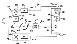
FIG. 24 is a block diagram showing ~yl-~ ullu~ detector 200 of the present invention.
Synchronous detector 200 includes detector input terminal 202 (at which a modulated carrier
signal is received) and detector output terminal 204 (at which a ~' - ' ' ' output signal is
provided). Detector 200 includes first mixa circuit 206 and second mixer circuit 208. A first
input 206a, 208a from each of frrst and second mixer circuits 206, 208, ~ ely, is
coMected to detector input temlmal 202. First mixer
~`W~ q~/~4~
- ~ 2186~3 ~ 996
- 18 -
output 206c from first nuxer circuit 206 is connected to detector output terminal 204.
Synchronous detector 200 ncludes phase transformer 210, sometimes referred to as a Hiibert
filter, which provides a 90 phase shift from input 210a to output ~iOb. The output of phase
transformer 210 is connected to second input 206b of first mixer circuit 206, and input 210a
to phase ~ rul.ll~ 210 is connected to second input 208b to second mixer circuit 208.
Synchronous detector 200 also includes voltage-contro~ied osciliator (VCO) 212 having an
oscillator input 212a and oscillator output 212b, osciliator output 212b being connected to
pnase tr~nsformer input 210a. Each of the first and second mixer circuits 206, 208 includes
a mixer element 206M, 208M, respectively, and a mixer filter element 206F, 208F,. Mixer filter elements 206F, 208F function only as low pass filters of the typedes~ibed with reference to FIG. 4D. There is no need to limit the bandwidth of mixer filter
element 208F to define a loop bandwidth for a phase-locked loop, as is required in
~u,.~...Liull,d synchronous detector 100 shown in FIG. 23.
Synchronous detector 200 includes combiner circuitry 220 which has first and second
combiner inputs 220a, 220b and combiner output æoc. First combiner input 220a isconnected to first mixer circuit output 206c, and second combiner input 220b is connected to
second mixercircuit output 20&. Synchronous detector 200 further includes loop filter 214
having loop fiiter input 214a and loop filter output 214b. Combiner output æoc is connected
to loop filter input 214a, and loop fiiter output 214b is connected to osciliator input 212a.
Combiner circuitry 220 includes jitter nqnr~ q~ n filter 224 and summer 222. Jitter
cancellation filter 224 has an input connected to combiner input 220a and an output connected
to a first input of summer 222. A second input of summer æ2 is connected to second
combiner input 22Ob. An output of summer 222 is connected to combiner output 220c.
rltter cance~iation fiiter 224 preferably includes high pass fiiter 228 and scaiing circuit 226.
Scaiing circuit 226 might preferably be a resistor, although it may include an amplifier of
t}ansfer function K.
Low pass fiiters 206F and 208F are designed to have cutoff frequency sufficient to remove
oniy the double carrier frequency content of the mixer output as shown in FIG. 4D. Volt~ge-
controlied oscillator 212, mixer 208, summer 222 and loop filter 214 form a phase-
~ 21~ 6 85 3 ' li ,
- 19-
locked loop (PLL). The loop bandwidth is defined by loop filter 214 according to desired
noise-bandwidth traieoffs since mixer filter element 208F does not necessarily limit signal
bandwidth. Phase jitter inherent in a vestigial sideband modulated signal (or even in a single
sideband signal) as received at the detector input terminal 202 is at least partially cancelled in
combiner circuit 220. Because of this feature, the bandwidth of loop filter 214 need not be
reduced in order to minimize tracking errors due to the inherent phase
modulation of a vestigial sideband modulated signal.
In op~ration, the signal at second mixer circuit output 20& is a replica to the signal at the
output of imagulary arm 18 of the VSB filter of mo~ulator 10 (FIG. 7). The frequency
response of imaginary arrn 18 (as shown iri FlGS. 20 and 22) is also of the same form as
shown in FIG. 25 as curve A. S~ ~i on ~his graph (at curve B) is the frequency
~sponse of a first order ~ . ' high-pass filter with a cut-off fr~uency of 0.1 Hz and
with the gain adjusted by 1/2 (i.e., -6dB) to be shown as a close match between thc two
response curves. FIGS. 26 and 27 are graphs showing the magnitude and phase response,
respectively, of this first order r .. high-pass filter over a more e~tended frequency
range. However, it should be noted that the range of interest for the ~, ' detector
shown n rlG. 24 is limited to the bandwidth of the loop filter. Over the bandwidth of the
loop filter, jitter c~Pll~ n filter æ4 is a close ~ to the frPquency response
shown in FIG. 20 at like r ~ ' Jitter - filter 224 may use any filter design
so long as its frcquency response is a close match to the spec~al power distribution of the
signal at second mixer circuit output 20&.
When VCO 212 is tuned to the carrier frequency the magrutude of the signal produced at
second mixer circuit output 20& is shown by curve A in FIG. 25. The magnitude is very
small for frequencies ne3r the center frc~quency and larger for fr^quencies further dist3nt from
the center frequency. r,..~ ,lc, the phase at positive frequency differences differs from
the ph3se at negative fre~uency differences by 180.
The signal at first mixer circuit output 206c is a replica of the signal at the output of real
arm 16 of the VSB filter of VSB modulator 10 (E~IG. 7). The spectral power of this replica
signal is of the same form as the frequency response of real arm 16 as shown in FIG. 18.
This replica signal is p3ssed through jitter ~nnPl~ n filter 224. The magrutude and
~V0 951~1330 2 ~ $ fi ~ ~ ~ p~ ~ c
- 20 -
phase response of jitter 'Iq~ n filter 224 is shown in FIGS. 26 and 27 ~ .y,
when the jilter ~ -n filter is based on the first order Bu~t~ .J~ filter described
above . The spectral power of the signal at the output of jitter ~ - .. r ll: ;. n filter 224 is shown
by curve B in FIG. 25 when jitter " filtçr 224 is based on the first order
Butterworth filter described above.
Thus, the frequency response of thc signal at the output of the jitter r~ r~llqtinn filter
224 is a close ~ for the frequency response of the signal at second mixer circuit
output 208c, at least in the lower frequency region. It should be noted that the filter need
not be limited to a first order r,. ~JIIll filter. Any order filter and other filter types may
be used so long as FIG. 25 curves A and B are rr ' ' ~ matched.
Summer 222 adds the signal at the output of jitter, 'l~inn filter 224 to the signal
provided at second mixer circuit output 208c. The po~ver s~ectrum of the resulting output
signAI of summcr 222 is shown as curve B in FIG. 28. Curve A of FIG. 28 shows the
output signal power spectrum with jitter " filter :' ' a.e., gain equal to
zero). Curve A, therefore, ~UI~O~rAJ~ to the frequency response shown in FIG. 20.
However, curve B is more subtle. The magnitude and phase of the signal input to
jitter n~ filter 224 w.lc r ' to the response curves shown in FIGS. 18 and 19,I,,o~L;~,l~. The phase near the center frequency is zero. Such a signal is then filtered in
jitter ~ ;,)n filter 224 having magnitude and phaso responses shown in FIGS. 26 and
27, respectively. At frequencies far displaced from the center frequency, the phase of the
signal at the output of jiKer ~ rl~ -- filter is still zero. In contrast, the phase of the
signal (curve A, FIG. 28) at second mixer circuit output 208c is either plus or minus 90 at
frequencies displaced from the center frequency. This is shown in FIGS. 20 and 21 for the
signal at the output of imaginary arm 18 of the VSB filter which ~ to the signaloutput from second mi~er circuit output 208c. Thus, there is a 90 phase difference betwoen
the signal at the output of jiKer ' - filter 224 and the signal at second mixer circuit
output 208c at frequencies far displaced from the center frequency. Since this 90~ phase
difference prevents signal .,~ the magnitude of curve B (FIG. 28) remains large at
frequencies far displaced from the center frequency.
w04s/27330 ~ 1,,,, /o~7?c
! 2 1 8 6 8 2 1
In contrast, at frequencies ne r the center frequency, the phase of the signal at the
output of jitter ran~Plla*nn filter 224 wl.~ r ' to tlle phase response of the high-pass filter
as shown in FIG. 27. At slightly positive ~ , ;, there is a pi-!s 90 phase shift, and
at slightly negative ~ , there is a minus 90 pllase shift. The phase of the signal
at seeond mixer eircuit output 208e ' to the phase response of the imaginary armof the VSB filter as shown in FIG. 21. At slightly positive frequencies, there is a minus 90
phase shift and at slightly minus fr~q--~nri~-~ there is a plus 90 phase shift. At frequencies
near the center frequency, summer 222 cancels the two input signals by adding two equal
magnitude signals, one having a plus 90 phase shift and the other having a minus 90 phase
shift. Thus, phase jitter inherent in a VSB signal is caneelled in eombiner circuitry 220.
However, true phase offsets in the VCO signal with respeet to the phase of the earrier signal
in the modulator are detected in second mixer eircuit 208 and passed through the loop filter
to adjust the VCO phase.
FIG. 28 is a graph showing the power spectrum of the signal at the input to the loop
filter. Depicted at eurve B is the power spectrum using the first order l~ult~ l ~. Jl l.h high-pass
filter with gain set to unity. Depicted at curve A is the power spectrum at the input to the
loop filter with the high pass filter ~' - ' (gain set to zero). FIG. 29 is a graph
showing an enlarged portion of FIG, 20. Note ~h~ that close to the carrier
frequeney, the noise density in the power spectrum is reduced by using the high-pass filter
design shown in FIG. 24 as eompared to old art without eombiner circuitry 220, thus
reducing phase jitter.
FlGS. 30 ar~d 31 illustrate the effect of the i system. If combiner circuitry
220 were connected into the modulator ~:IG. 7) so that the output of real arm 16 was
connected to the input of jitter ~ n~PII ~ *nn filter 224 (i .e., eombiner circuit Flrst input 220a),
and the output of imaginary arm 18 was ~' ' from mi~er 24 and connected to second
combiner cireuitry input 220b instead, and combiner eircuitry output 220c were eonnected
to mi~er 24 in place of the output from imaginary arm 13, the spectral power of the signal
at output terminal 14 would be as is shown in FIGS. 30 and 31. FIG. 30 shows theequivalent spectral power (as log magnitude) of the vestigial sideband modulated signal
referenced to baseband when the ~ of the first order B.. ;t~ -l, filter are used
;~Tf~ ~5~n
2~68~3
- 22 -
in the combiner circuitry 220. Curves A-E correspond to jitter rr~nrrll~rir,n filter gains of 0,
.5, .75, 1.0, and 1.25, respectively. FIG. 31 is a graph showing an enlarged portion of the
frequency response curve near the carrier frequency. ~n order to minin~ize phase jitter, it is
desirable that the frequency response near the carrier frequency be as flat as possible (e.g.,
culve C in FIG. 31) to counter the effects causing phase jitter as discussed ~vith referenoe to
FIGS. 6A-6D.
Therefore, jitter " filter 224 in conjunction with summer 222 in combiner
circuitry 220 are capable of canoelling the phase jitter inherent in vestigial sideband and other
signals at trequencies near the carrier frequency on the transmitter side as well as the receiver
side. Ihis feahlre perrnits the bandwidth of the loop filter to be made wider while still
maintaining a specified phase tracking accuracy. It will be appreciated that the phase tracking
accuracy provided by the ~, ' detçctor shown in FIG. 24 may be improved comparedto old art when ~, a specified bandwidth for the loop bandwidth filter which maybe a ~ due for other system constraints.
The }" cl of the y - l..~ detectors sho vn in FIGS. 23 and 24 were simulated
on a computer for a 21.5 Mbit/sec. data stream in a 4-VSB format. FIGS. 32A-32D are
graphs and histograrns showing the simulation results for carrier recovery of 4jO00 simulated
symbols. The vertical scale of FIGS. 32A and 32B show the phase of the recovered carrier
of loop filter 214 (designed as a 13.4 k~, and N=2 low pass filter). FIG. 32A 'J" '' `l-''''l`
to the cu..~.,tiu.~ detector where the loop filter output, when converted into
degrees, varies between -1.2877 and + 1.4572 degrees with a mean and standard deviation
of 0.0003 and .4629 degrees. The c~nrP~ ;rm was , . ' by a high pass filter witha cut off frequency of 312.5 kHz. FIG. 32B shows the loop filter output with a jitter
,- ll,-i"" filter (designed as the 312.5 kHz high pass filter). The exoess filter bandwidth
(i.e., the alpha factor) is, in this example, 12 9~ . The loop filter output, when converted into
degrees, varies from a -0.2420 to +.2873 degrees with a mean and standard deviation of -
0.0021 and .0735 degrees. Thus, ~.~hu..ous detector 200 shown in FIG. 24 reduoes peak-
t~peak phase jit~er as compared to w.~ ' detector 100 by a factor of more
than 6 to I (See FIGS. 32C and 32D for histograms of the phase of the recovered carrier).
In practical reoeiver systems, the improvement enables reliable reoeption of signals with less
distor~ion (e.g.,
~. ~ r.. ~
w0 9s/27330 ~ ; 3 t~ U,~ 2 !~c
- 23 -
distortion ~nown in the television arts as quadrature distordon). A different filter design
which would result in a closer match '.~etween curves A and B in FIG. 25 would furtner
improv~ ~rformance. More , ;, and therefore more e~pensive, filter designs may
provide better ~ r but might incre_se the cos~ and complexity of the ~.,I.lvl.vus
detector. It is left to tle designer to select the filter design for t.2e jitter . ~ flter
which provides the best phase tracking l r consistent with t, e design constraints of
cost, complexity and other constraints imposed by the p~,rticulAr teci nology being used in the
,J...,II-u,~ou~ detector (e.g., digital vs. analog circuits, bipolar vs. MOS tr~nsistors, etc.).
In FIG. 33 modulator 3v0 includes rea, and imaginary arm filters 16 and 18 and
transmitter ,-; 'lqti~2n circuit 310. Tr~nsmitter - 'lqti~2n circuit 310, ~ 2~1"2g tû
combiner circuitry 220 (EIG. 24) includes high pass (or band pass) flter 312, amplitude
scaling circuit 313, and summer 314. The output of summer 314 provides the signa. input
to second mixer 318 and reAI arm 16 provides the . r signa, input to first mixer316. Modu ator 300 nay substitute for the modu ator depicted in FIG. 7 to control the shape
of the spectrum as discussed with reference to FIGS. 3~ and 31.
Havine described preferred r .. .~l . t~ of a nolrel ~.r ' detector and method
for ~ ;..v..v..~ detection, which are intended to be illustrative and not limiting, it is noted
that ....~ ;.."c and variations can be made by those slcilled in the art in light of the above
teachings. It is therefore to be understood that changes may be made in the particular
of the invention dirclosed which are within the scope and spirit of the inven~ion
as defned by the appended claims.
Having thus described the invention with t;,e detAils and ~U~U;AUily required by the
patent laws, what is claimed and desired protected by _etters Patent is set forth in the
following claims.