Note: Descriptions are shown in the official language in which they were submitted.
= WO 96125778 PCT/US96101033
1 2186899
. . ,;
PULSE POWER GENERATING CIRCUIT WITH -
ENERGY RECOVERY
BACKGROUND OF THE INVENTION
1. Field of the Invention
The present invention relates generally to pulse power sources
and more particularly, to an apparatus and method for providing high
voltage pulse power and energy recovery for use in excimer and other
pulsed lasers.
2. Description of the Prior A*t
In applications where pulsed lasers are operated for extended
periods of time, there is a need for energy efficiency, long term
reliability and high component lifetimes. In these applications,
magnetic compression circuits in conjunction with solid state switches
have recently been utilized to supply pulse power because of the
reliability and useful life of the magnetic compression circuits and
solid state switches.
Such magnetic compression circuits generally utilize a multi-
stage LC network to provide the power compression. Various
techniques exist for increasing the power output of such devices,
including the use of complicated pulse generating networks such as
that described in U.S. Patent No. 5,138,622 to Friede et al. and the use of
multi-stage magnetic modulators to achieve a high packing factor.
These techniques, however, are complex and expensive to implement
and their use provide long term unreliability. Specifically, they are
energy inefficient and promote short laser component life-times. For
example, after the laser discharges, energy left in the circuits is
dissipated in the laser, resulting in reduced electrode life.
CA 02186899 2006-02-08
-2a-
Accordingly, in one aspect, the present invention provides a pulse
power generating circuit comprising: a capacitor for storing a charge; a
magnetic pulse compressor circuit; a switch coupled at one end to said
capacitor and another end to said magnetic pulse compressor circuit, for
periodically applying the charge stored in said capacitor as an input to said
compressor circuit, the compressor circuit providing an output pulse in
response to the input, said compressor circuit also resonantly providing a
reverse charge that is reflected from a load coupled to said compressor
circuit;
and an inverting circuit coupled in parallel with said capacitor for storing
and
inverting said reverse charge to obtain an inverted charge, said inverting
circuit also providing said inverted charge to said capacitor through said
switch during a next pulse.
In a further aspect, the present invention provides a method of
generating pulse power, comprising the steps of: storing a charge in a
capacitor; periodically applying the charge stored as an input to a magnetic
pulse compressor circuit; providing an output pulse in response to the input,
said compressor circuit also resonantly providing a reverse charge that is
reflected from a load coupled to said magnetic pulse compressor circuit;
recovering said reverse charge by inverting said reverse charge to obtain an
inverted charge; and providing said inverted charge to said capacitor during a
next pulse.
In a still further aspect, the present invention provides a high-voltage
pulse power laser system, comprising: a power source for supplying charge; a
capacitor for storing said charge; a magnetic pulse compressor circuit; a
solid
state switch coupled at one end to said capacitor and at a second end to said
magnetic pulse compression circuit, for periodically applying the charge
stored in said capacitor as an input to said compressor circuit, the
compressor
circuit providing an output pulse in response to the input, said compressor
circuit also resonantly providing a reverse charge that is reflected from a
load
coupled to said magnetic pulse compressor circuit; a laser coupled to said
CA 02186899 2007-05-11
-2b-
magnetic pulse compressor circuit, said laser receiving said output pulse; and
an
inverting circuit coupled in parallel with said capacitor for storing and
inverting said
reverse charge to obtain an inverted charge, said inverting circuit also
providing said
inverted charge to said capacitor through said switch.
In a further aspect, the present invention provides a high voltage pulse power
laser system comprising: a power source; a pulse compressor circuit having a
solid state
switch coupled to said power source; and a laser coupled to the output of said
pulse
compressor circuit; said pulse compressor circuit providing compressed power
to said
laser in response to power input from said power source through the solid
state switch,
said compressor circuit also recovering energy not used in said laser by
reversing the
unused energy and returning the recovered energy to said power source.
In a still further aspect, the present invention provides a method of
recovering
energy in a laser system, comprising the steps of periodically applying a
charge as an
input to a pulse compressor circuit; providing an output pulse to said laser
system in
response to the input, said compressor circuit also resonantly providing a
reverse charge
that is reflected by said laser system; recovering said reverse charge by
inverting said
reverse charge to obtain an inverted charge; and providing said inverted
charge as part of
the input to said compressor circuit in a next output pulse.
In a further aspect, the present invention provides a high voltage pulse power
laser system comprising: a power source; a capacitor for storing a charge; a
pulse
compressor circuit having a solid state switch coupled to said power source;
and a pulse
discharge laser coupled to the output of said pulse compressor circuit; an
inverting circuit
coupled in parallel with said capacitor for storing and inverting a reverse
charge that is
reflected by said pulse discharge laser; said pulse compressor circuit
consistently
providing
CA 02186899 2006-02-08
-2c-
compressed power to said laser without missed pulses in response to power
input from said power source through the solid state switch.
In a still further aspect, the present invention provides a pulse power
generating circuit comprising: a capacitor for storing a charge; a
magnetic pulse compressor circuit having at least one stage, said at least
one stage comprising a capacitor and a saturable inductor; a biasing
circuit for encouraging the inductor of the at least one stage into reverse
saturation; a switch coupled at one end to said capacitor and another end
to said magnetic pulse compressor circuit, for periodically applying the
charge stored in said capacitor as an input to said compressor circuit, the
compressor circuit providing a forward current output pulse in response
to the input, said compressor circuit maintaining a forward current while
resonantly providing a reverse charge which is reflected from a load
coupled to said compressor circuit; and an inverting circuit coupled in
parallel with said capacitor for storing and inverting said reverse charge
to obtain an inverted charge, said inverting circuit also providing said
inverted charge to said capacitor through said switch during a next
pulse.
In a further aspect, the present invention provides a method of
generating pulse power, comprising the steps of: storing a charge in a
capacitor; periodically applying the charge stored as an input to a
magnetic pulse compressor circuit having at least one stage, said at least
one stage comprising a capacitor and a saturable inductor; providing a
biasing circuit for encouraging the inductor of the at least one stage into
reverse saturation; providing a forward current output pulse in response
to the input, said compressor circuit also maintaining a forward current
while resonantly providing a reverse charge that is reflected from a load
coupled to said magnetic pulse compressor circuit; recovering said
CA 02186899 2006-02-08
-2d-
reverse charge by inverting said reverse charge to obtain an inverted
charge; and providing said inverted charge to said capacitor during a
next pulse.
In a still further aspect, the present invention provides a high-
voltage pulse power laser system, comprising: a power source for
supplying a charge; a capacitor for storing said charge; a magnetic pulse
compressor circuit having at least one stage, said at least one stage
comprising a capacitor and a saturable inductor; a biasing circuit for
encouraging the inductor of the at least one stage into reverse saturation;
a solid state switch coupled at one end to said capacitor and at a second
end to said magnetic pulse compression circuit, for periodically applying
the charge stored in said capacitor as an input to said compressor circuit,
the compressor circuit providing a forward current output pulse in
response to the input, said compressor circuit also maintaining a forward
current while resonantly providing a reverse charge that is reflected
from a load coupled to said magnetic pulse compressor circuit; a laser
coupled to said magnetic pulse compressor circuit, said laser receiving
said output pulse; and an inverting circuit coupled in parallel with said
capacitor for storing and inverting said reverse charge to obtain an
inverted charge, said inverting circuit also providing said inverted
charge to said capacitor through said switch.
In a further aspect, the present invention provides a high voltage
pulse power laser system comprising: a power source; a pulse
compressor circuit having a solid state switch coupled to said power
source, said pulse compressor circuit also having at least one stage, said
at least one stage comprising a capacitor and a saturable inductor; a
biasing circuit for encouraging the inductor of the at least one stage into
CA 02186899 2006-02-08
-2e-
reverse saturation; and a laser coupled to the output of said pulse
compressor circuit; said pulse compressor circuit providing compressed
power to said laser in response to power input from said power source
through the solid state switch, said compressor circuit providing a
forward current output pulse in response to the power input, said
compressor circuit also maintaining a forward current while resonantly
recovering energy not used in said laser by reversing the unused energy
and returning the recovered energy to said power source.
In a still further aspect, the present invention provides a method of
recovering energy in a laser system, comprising the steps of:
periodically applying a charge as an input to a pulse compressor circuit
having at least one stage, said at least one stage comprising a capacitor
and a saturable inductor; providing a biasing circuit for encouraging the
inductor of the at least one stage into reverse saturation; providing a
forward current output pulse to said laser system in response to the
input, said compressor circuit maintaining a forward current while
resonantly providing a reverse charge that is reflected by said laser
system; recovering said reverse charge by inverting said reverse charge
to obtain an inverted charge; and providing said inverted charge as part
of the input to said compressor circuit in a next output pulse.
In a further aspect, the present invention provides a high voltage
pulse power laser system comprising: a power source; a capacitor for
storing a charge; a pulse compressor circuit having a solid state switch
coupled to said power source, said pulse compressor circuit also having
at least one stage, said at least one stage comprising a capacitor and a
saturable inductor; a biasing circuit for encouraging the inductor of the
at least one stage into reverse saturation; a pulse discharge laser coupled
CA 02186899 2007-05-11
-2f-
to the output of said pulse compressor circuit; and an inverting circuit
coupled in parallel
with said capacitor for storing and inverting a reverse charge that is
reflected by said
pulse discharge laser; said pulse compressor circuit consistently providing
forward
current compressed power to said laser without missed pulses in response to
power input
from said power source through the solid state switch, said pulse compressor
circuit
maintaining a forward current while resonantly providing a reverse charge
which is
reflected from the pulse discharge laser.
In a still further aspect, the present invention provides a method of
generating
pulse power, comprising the steps of: storing a charge in a capacitor coupled
to a second
capacitor; periodically applying the charge stored as an input to a magnetic
pulse
compressor circuit; providing an output pulse in response to the input, said
compressor
circuit also resonantly providing a reverse charge that is reflected from a
load coupled to
said magnetic pulse compressor circuit; recovering said reverse charge by
inverting said
reverse charge to obtain an inverted charge; and providing said inverted
charge to said
capacitor during a next pulse.
WO 96/25778 3 2186899 PCTIUS96/01033
..^
i==j~~il~. _- .,.
BRIEF DESCRIPTION OF THE DRAWINGS
Figure 1 is a schematic diagram of a preferred embodiment of
the pulse power generating circuit of the present invention.
Figure 2 is a schematic diagram of an alternate embodiment of
the pulse power generating circuit of the present invention.
Figure 3 is a graphical representation of the relationship between
the flux density and field strength in a typical saturable core inductor.
Figures 4A - 4E are timing diagrams illustrating the energy
transfer and recovery cycles in the pulse power generating circuit of the
present invention.
Figure 5 is a perspective view of a laser system utilizing the
pulse power generating circuit of the present invention.
DETAILED DESCRIPTION OF THE INVENTION
The present invention relates to a pulse power generating circuit
which is capable of recovering energy that otherwise would be wasted
in a system through a transfer of the dissipated energy back into the
power source of the system.
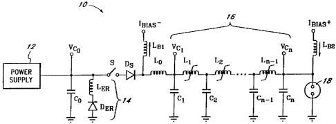
Figure 1 is a schematic diagram of a preferred embodiment of
the pulse power generating circuit 10 of the present invention. The
pulse power generating circuit 10 comprises a high voltage DC power
supply 12, an energy storage capacitor Co, an inverting circuit 14, a solid
state switch S and a pulse compressor circuit 16 for compressing the
duration and increasing the voltage of pulses applied. The pulse
power source is coupled to a load 18, typically a pulse discharge load
such as an excimer laser.
Figure 2 is a schematic diagram of an alternate embodiment of
the pulse power generating circuit 10 illustrated in Figure 1. In this
alternate embodiment, a step up transformer 20 is coupled to the
WO96125775 PCT/US96/01033 =
-4-
~186899
output of the compression circuit 16. Alternatively the transformer 20
may instead be coupled to the power generating circuit at one of
several nodes (for example, nodes 1, 2, ...n) in the pulse compressor
circuit 16, depending on design requirements. A transformer 20
coupled to the circuit 10 at a node closer to the power supply 12 will
subject downstream components of the pulse compressor circuit 16 to a
higher voltage but lower current than the embodiment of Figure 2, and
of course will effect the design of such components because of the
different impedance and other operating conditions they will be
subjected to. Conversely, a transformer 20 coupled to the circuit 10 at
a node closer to the load 18 will allow use of low voltage but high
current components supplying the transformer. Further the
transformer itself can be somewhat different, depending on its
placement, as stepping the voltage up to the desired high level before
the final pulse compressor reduces the required peak current
capabilities of the transformer.
In a preferred embodiment, the power supply 12 is a 0-1 K volt
D.C. power supply, with the pulse power supply providing an energy
per pulse of 2 Joules in a pulse width of 100 nanoseconds at
approximately a 1 Khz pulse rate. The D.C. supply 12 is used to charge
capacitor Cp, shown as a single capacitor, though typically comprising a
bank of parallel corutected capacitors. For instance, to obtain a 16
microfarad capacitarice for capacitor Cp, 160 0.1 microfarad, 1000 volt
capacitors may be connected in parallel.
The switch S may be a silicon controlled rectifier (SCR), an
insulated-gate bipolar transistor (IGBT), a metal-oxide semiconductor
field-effect transistor (MOSFET), a MOSFET coiitrolled thyristor (MCT),
or any other suitable switching element as known in the technology.
The pulse power generating circuit 10 preferably comprises a diode D5
connected in series with the switch S. The inclusion of Ds in the
circuit 10 ensures that the circuit 10 is nonconductive with respect to
reverse current, as will be described in detail in the section below. In
another preferred embodiment, the pulse power source 10 further
comprises an inductor LO selected in conjunction with CI to provide a
WO 96/25778 PCT/US96101033
W ;~r 5 2186899
time constant for the LC combination to slightly slow the buildup of
current flow through the switch S so that the switch may become
completely closed prior to high current flow through the switch. This
substantially reduces power dissipation in the switch, conserving
~ energy and reducing the heating in the switch and peak current
conduction requirement of the switch to reasonably manageable levels.
However, it provides a current pulse through the switch which is too
low in current and too long in duration to itself provide the intended
output for the pulse power source without pulse compressor, provided
by the rest of the circuit.
In a preferred embodiment, the switch S is a solid state switch
such as an SCR switch. The use of an SCR switch in the pulse power
generating circuit 10 of the present invention in a laser offers a distinct
advantage. Specifically, it was found that laser systems utilizing the
pulse power generating circuit 10 with an SCR switch generate pulses
consistently. In fact, the pulse power generating circuit 10 utilizing an
SCR switch does not provide even a single missed pulse throughout
the life of the laser. This is because SCR switches do not suffer from
gradual degradation nor exhibit prefire behavior, as will be discussed in
greater detail in the following sections.
The pulse power source 10 also includes bias inductors Lgl and
LB2, each of which is connected at one end to a current source, IgIAS-
and IgIAS+ respectively, and at the other end, to compressor circuit 16.
As shown in Figure 1, a negative current relative to the desired output
pulse is used to bias the compressor circuit 16, as will be discussed in
greater detail below. The bias current is supplied through inductors of
relatively high inductance to provide relatively high time constants in
the bias circuit relative to the pulse rate of the pulse power source to
isolate the bias current source from the pulse power source itself.
Energy recovery is facilitated in part by inverting circuit 14 which
comprises inductor LER and energy recovery diode DBR.
The compressor circuit 16 comprises banks of capacitors Cl, C2, Cn-1 and Cn
and one or more saturable core inductors Ll, L2,..., Ln-1
WO 96/25778 PCT/US96/01033
c ;,,- -6- .2185899 ~
connected in a ladder network. As shown in Figure 1, a first saturable
core inductor Ll is connected between CI and C2, a second saturable
core inductor L2 may be connected in series between C2 and C3,..., and a
saturable core inductor Ln_1 is connected in series between Cõ_1 and Cn.
The circuit of Figure 2 is identical to that of Figure 1 with the
exception of the addition of the step up transformer 20 shown between
the output of the pulse power source and the load 18, for the preferred
embodiment an excimer laser, though the step up transformer may be
inserted in circuit at Cl or any of the capacitors between Cl and C. The
presence and location of the transformer does not effect the function of
the other components of the pulse power supply, though being an
impedance transforming device (transforming voltages and currents),
the values, current capacities and voltage capabilities of the
components from and including the power supply 12 to the primary of
the transformer will differ substantially from the corresponding
components of Figure 1, even though the same will normally be
chosen to have substantially the same time constants as the
embodiment of Figure 1.
The method of operation of the present invention will now be
discussed. Figure 3 is a graphical representation of the relationship
, I
between the flux density B and magnetizing force per unit length NV
characteristic of the major hysteresis loop of a saturable core inductor,
where N in the number of inductor coil turns on the core, I is the
length of the core and i is the current in the inductor.
In addition, the total flux (D in the saturable core is given by the
equation:
0 =BA (1)
where B is the flux density and A is the cross-sectional area of the core.
As also known in the technology, the relationships between the
electromotive force (emf) induced in a coil having N turns, the rate of
WO 96/25778 PCTIUS96l01033
~.,.
~ a 2186899
change of flux in the core about which the coil is wound and the rate of
change in current in the coil are:
d = L dt
e=N
dt dt (2)
where L is the inductance of the inductor.
Substituting equations (1) into equation (2), we have
NdO=Nd(BA) (3)
dt dt
Thus,
Lr=NA~B (4)
L = NA dB (5)
di
Thus, the inductance L of a coil is directly proportional to the
rate of change of B with respect to i.
Thus, with reference to Figure 3, the value of dB and thus the
inductance when the inductor is operating along the line a-b, the line
c-d and anywhere along the line c-e of the curve is small, since the
gradient of the curve is slight. However, the value of ~B is large along
line b-c and line d-a where the gradient of the curve is steep. Thus,
starting at point a (set by the negative bias current IBIAS - see Figures 1
and 2), L is relatively small along line a-b. However, once enough
current passes through the inductor coil in the positive direction to
start to substantially change the magnetization of the core, the
inductance L of the inductor suddenly greatly increases, as shown by
the change of I at point b. The inductance remains large until point
c is reached, at which time the inductance returns to a low value,
allowing the current through the inductor to rapidly rise to point e and
beyond, and to later return to point d, all in accordance with the
WO 96/25778 PCT/US96/01033
-s-
218b899
voltage across the inductor. Between point e and point a, the
inductance is again relatively high.
The method of the present invention provides a bias current
from IBIAS- and IBIAS+ through LB1 and LB2 to the compression circuit
16 to ensure that the saturation inductors Ll, L2,...Ln-1 are biased to
operate along line c-e of the curve as shown in Figure 3. This ensures
that the current passing through saturable inductors Ll, L2,...Ln-1 is
conducted in one direction for energy recovery. It also ensures a large
time constant for each LC stage of the compression circuit 16 so that
sufficient time is p"rovided for full energy transfer from one capacitor
(e.g., Cl) to another (e.g., C2) through the inductor (e.g., LI). At the end
of a transfer cycle, the inductors Ll, L2.... Ln_1 are biased to ensure that
their corresponding inductance is reduced to that at point a in Figure 3,
so that proper biasing of the inductors Ll, L2,...Ln_I may be
accomplished during the next pulsing cycle. Specifically, the
inductance of the inductors Ll, L2,...Ln-1 must increase with the
corresponding increase of positive or uni-directional current in the
inductor, as will be discussed in detail below.
The operation of the pulse power generating circuit 10 will be
described with reference to Figure 3 and the timing diagrams
illustrated in Figures 4A-4E. With the D.C. power supply 12 on prior
to the time t0 (when switch S is open), capacitor CO is charged by the
current supplied by the D. C. power supply 12. When fully charged,
the voltage acrosscapacitor Co is VCp (see Figure 4A). At to, the switch
S closes, and the energy stored in capacitor Co is transferred to Cl (see
Figure 4B) by action of the LC circuit comprising Lp, Co and CI with a
( ii~
time constant of approximately I LOCOCI )~ Cl becoming nearly fully
\ o i
charged and the current in inductor Lp reducing substantially but still
remaining positive at time tl. Inductor Lp is included in the circuit to
purposely provide a sufficiently large time constant in this energy
transfer to ensure tl-iat S is fully switched before high currents are
encountered, and to limit the maximum current through the switch
for a given energy transfer to a value manageable by a solid state switch
WO 96/25778 PCT/US96101033
9 218b899
by extending the time of the transfer. As capacitor Co starts to discharge
through switch S and capacitor Cl begins to charge during this transfer,
the current in the coil of saturable inductor Ll rapidly changes from the
negative bias current of point a to the low positive current of point b of
Figure 3, at which point the inductance jumps to a relative high value
to limit the rate of further current increase through Ll.
At time tl, while the current in inductor Lo is low but still
positive, the saturable core of inductor Ll saturates, at which time the
inductance of inductor Ll jumps to a low value, allowing the current
there through to rise to a very high value to transfer the energy from
capacitor Cl to capacitor Cg with a time constant approximately equal to
r i/2
L15C'C21 , where L,, is the inductance of the inductor Ll with the
CI+CZ/
core in saturation (line c-e in Figure 3). Note that this time constant
1/2
may be substantially shorter than the time constant ( 11 because
l o J/
I.is may be made much less than L0.
In the manner described above, energy is transferred through
each stage of the compressor circuit 16, if more than one stage is used,
compressing the pulse in time in one or more stages as desired, and if
of low voltage originally, being stepped up in voltage where desired.
When Cn-1 is substantially fully charged and the core of inductor Ln-i
saturates, the energy is coupled through the saturated inductor from
Cn-1 to Cn in a short time period pulse, with the voltage across Cn being
applied to the laser 18.
At time tL, the voltage across Cn builds to the level required to
initiate discharge in the laser, and the laser 18 fires. Energy stored in Cn
and still being fed to Cn through the inductor is delivered to the laser
discharge in the compressed time period of the pulse power supply (see
Figure 4E). After discharging, Cn is driven negative. When this
occurs, Ln-1 is already saturated for current flow from Cn-1 to Cn. Thus,
instead of having energy ringing in the laser 18, ernding the electrodes,
the saturated state of Ln-1 causes the reverse charge on Cn to be
transferred resonantly back into Cn_i as shown in Figure 4D. This
WO96/25778 PCTlUS96101033
10- ~i8 6
8 9 9
transfer is accomplished by the continued forward flow of current
through Ln_1 .
When energy is transferred back into Cn_l, Cn_1 is driven
negative with respect to Cn_z. This process repeats back up the L-C
ladder network of the pulse compressor circuit until the energy which
would have been destructively dissipated in the load 18, is transferred
from Cn_i to Cn_z.This transfer process continues until the energy in
Cn is passed to Co, as shown in Figure 4A. It should be noted that such
reverse energy transfer is possible only if all saturable inductors Ln, ...
Ln_1 remain forward conducting to operate along curve c-e of Figure 3,
since the voltage of Cn with respect to Cn_I (and similarly, Cn-i with
respect to Cn_y ... etc.) must be negative for the energy propagation to
be accomplished. Thus, an important factor in the design of the pulse
power generating circuit 10 is that all the coils of all saturable inductors
Ll, L2,...Ln_1 must be forwardly conducting to operate in the proper state
for one way current transfer until waste energy is fully recovered.
When the waste energy is propagated back into Co, Cp is driven
negative with respect to its initially stored charge, and switch S is
opened. The inverting circuit 14, comprising an inductor LER and a
solid state diode DgR coupled to ground reverses this polarity through
resonant free wheeling - a half cycle of ringing of the LER-CO circuit as
clamped against reversal of the current in inductor LER by diode DER,
with the net result that the energy is recovered by the partial
recharging of capacitor Cp, thereby the energy which otherwise would
have contributed to erosion-of the laser electrodes and reducing the
supply requirements of the D.C. power supply.
The pulse power generating circuit of the present invention may
be utilized in lasers which operate on the principle of transverse
discharge. These lasers include systems which discharge at high
pressure, such as CO2 lasers, copper vapor lasers and excimer lasers
including KrF ezcuner lasers. Figure 5 illustrates a laser module 20
which may utilize the pulse power generating circuit 10 (enclosed in
chassis 22) of the present invention as a power source. A typical
WO 96/25778 PCT/US96101033
11 2186899
example of such a laser includes the HPL-100 laser module
manufactured and sold by Cymer Laser Technologies, assignee of the
present invention.
Several advantages exist through the application of the pulse
power generating circuit of the present invention. First, by using the
pulse power generating circuit, the energy efficiency of a laser system is
increased while electrode erosion from after discharge ringing is
minimized, since the waste energy which would otherwise be left
ringing in the laser 18 is effectively removed from the laser 18. The
energy reflected by the laser chamber due to impedance mismatch no
longer rings back and forth between the pulse power generating circuit
and the laser chamber since this energy is recovered by the pulse power
generating circuit of the present invention. As described, the pulse
power generating circuit is designed to transmit this reflected energy all
the way back through the pulse forming network into Cp. Upon
recovery of this energy onto Cp, the switch turns off, ensuring that this
captured energy remains in Cp. Thus, regardless of the operating
voltage, gas mixture or chamber condition, the voltage waveform
across the laser electrodes exhibits the behavior of a well-trained
system. This performance is maintained over all laser operating
conditions.
As discussed, after-ringing has been found to have a detrimental
impact on the laser chamber's electrode lifetime. After the main laser
discharge, current flow between the chamber electrodes becomes
nonuniform and breaks up into localized areas of high current density
called streamers. Elimination of this after-ringing by the solid state
pulse power generating circuit starves the streamers of energy and
reduces the amount of electrode damage caused by these streamers.
Secondly, by incorporating an SCR switch in a preferred
embodiment of the pulse power generating circuit of the present
invention, prefiring in the laser system can be eliminated while
predictability and reliability of the laser system can be increased. This is =
because SCR switches, unlike conventional thyratron switches, neither
WO 96/25778 12 2 1 868 ~P,CT/US96/01033 ~
/
suffer from gradual degradation nor exhibit prefire behavior.
Specifically, the use of SCR switches in pulse power generating circuits
has been demonstrated to last for greater than 30 billion pulses under
typical operating conditions without a single missed pulse or failure of
the pulse power generating circuit. In addition, experimental results in
a prototype of the pulse power generating circuit of the present
invention has thus far accumulated in excess of 6 billion pulses
without a single failure or missed pulse. It has also been determined
experimentally that i:he pulse power generating circuit of the present
invention exhibits the same efficiency at 6 billion pulses as it did at 300
million pulses. -
Thirdly, the use of the solid state pulse power generating circuit
of the present invention in a laser has increased the useful chamber
life of the laser by 100%, from 3 billion pulses to 6 billion pulses,
without any degradation in performance.
Finally, three other factors are significant in the reduction of cost
of operation in using a solid state pulse power generating circuit
instead of a thyratron-based pulse power system. The most significant
reduction in cost is a ten-fold increase in the expected lifetime of a laser
system using the pulse power generating circuit of the present
invention. The increase in expected lifetime is from 3 billion pulses
for a thyratron pulse power laser system to 30 billion pulses for a solid
state pulse power laser system. The second factor in overall system cost
reduction is the complete elimination of missed laser pulses and thus
the reduction in wafer level rework. The third factor involves a
reduction in downtime for laser service procedure. A thyratron-based
pulse power circuit used on a typical laser system must go through a 10
minute warm-up period to achieve proper thyratron temperature. The
solid state pulse power generating circuit of the present invention
requires no warm-up time, and thus each laser service procedure can
be shortened by approximately 10 minutes.
Although the invention has been described in terms of a certain
preferred embodiment, other embodiments apparent to those skilled
WO 96/25778 PCTlUS96/01033
2186899
in the art are also within the scope of this invention. Accordingly, the
scope of the invention is intended to be defined only by the claims
which follow.
. .r,T,f= r 1 i ~ i -i-}.