Note: Descriptions are shown in the official language in which they were submitted.
- 2186918
METHOD AND APPARATUS FOR REDUCING
DATA DELAY WITHIN A MULTI-CHANNEL
SHARED-CIRCUIT DATA PROCESSING ENVIRONMENT
BACKGROUND OF THE INVENTION
1. Field of the Invention
The present invention relates to a method and
apparatus for reducing group delay arising from the
processing of data within a mufti-channel, shared
circuit, data processing environment.
2. Description of the Related Art
Recently, considerable interest has developed
in the design of mufti-channel integrated circuits that.
include functional circuits which may be shared by the
circuit's multiple channels. By integrating operation
of a "shared" circuit with multiple channels (i.e., on a
single chip or chip set), the integrated circuit's
manufacturing cost may be reduced. More particularly,
the fewer circuits required within an integrated
circuit, the smaller and less complicated the design and
the physical dimensions of the circuit can be.
Telecommunications systems, and in particular,
digital voice transmission systems, frequently use
coder/decoders (CODECs) to convert data between digital
and analog form at each telephone subscriber's line.
CODECs convert analog signals, e.g., voice signals, to
pulse-code modulated (PCM) digital signals and digital
PCM signals to analog. Evolving circuit technology
first provided single CODEC integrated circuits (for use
by a single channel) and then multiple channel
2
- 2186918
integrated CODECs (Prior Art Figs. 1 and 2).
Thereafter, multiple channel integrated CODECs were
developed in which certain generic functional circuits
(generic to each channel's processing) were time-shared
between each of the CODECs multiple channels (Prior Art
Figure 3). By integrating the processing with a single,
shared functional circuit instead of N functional
circuits, reduction in per-channel cost is realized
because of the savings in space and effort required to
manufacture the N-1 duplicated circuits within a
conventional multi-channel device. Concomitantly, the
implementation cost of a system within which the shared-
circuit CODECs is reduced.
Figure 1 is a block-diagram depiction of a
portion of a conventional multi-channel integrated
circuit that includes decimators 2, 4, 6, 8, for each of
the circuit's four channels. Each of the decimators are
strobed simultaneously with a decimator synchronizing
signal to produce multiple contemporaneous outputs.
These outputs are fed into the individual buffers 12,
14, 16, 18, which release the buffered data (onto the
time division multiplexed bus) in accordance with
timeslot synchronizing signals generated and delivered
by the timeslot interchange 10.
Figure 2 is a block. diagram of another
depiction of a conventional multi-channel circuit where
each of the channels include decimators 32, 34, 36, 38,
that are strobed independently by decimator
synchronizing signals. The decimated data are output
thereby at different times, according to the PCM bus
' 3
_ ~ 18b91
definition for each channel. Such a design, however,
still requires dedicated decimator circuits for each
channel.
Figure 3 depicts a portion of a prior art
multiple channel CODEC that includes a decimator 40
shared by each of the CODEC's channels. Each channel's
data are generally output from the time-shared decimator
at an even rate, equally spaced in time, or in a burst
with channel samples output one after the other followed
by a dead time. Each channel's oversampled data are
directed to a timeslot interchange (TSI) 10 to adjust
the phase of the channel's data. The samples are passed
through the TSI to arrange timing consistent with TDMB
need, as described above with reference to Figure 1.
While multi-channel, shared-circuit CODECs are
attractive given their ability to time share at least
one functional circuit, such as filtering and encoding,
PCM data emerging from (or provided to) a shared circuit
typically requires some sort of time or phase adjustment
to accommodate system communication's parameters. To do
so, the channel-specific data output from (or input to)
the shared circuit is generally fed into a timeslot
interchange. The timeslot interchange adjusts the
data's phase for placement on a time division
multiplexed bus (TDMB). A problem inherent within such
multi-channel, shared circuit processing, however, is
that a delay i:, introduced into each channel's data
while it is phase-arranged to specific slots on the bus.
A group delay develops as an accumulation of delays,
limiting system performance.
4
218691$
For example, CODECs within each subscriber
line of a modern digital system typically encode and
decode PCM digital data at an 8 kHz rate within a given
timeslot, depending on communication system parameters.
Some systems use fixed assignments, while other systems
assign timeslots dynamically as calls are placed. A
problem with the conventional structure of a shared-
circuit multi-channel CODEC is that it directs data
to/from the shared circuit in particular time order,
e.g., first-in-first-out. The processed data typically
must be time arranged, leading to processing delay. The
time-arranging or resorting, in its worst case, can
impose up to a whole 8 kHz frame (i.e, 125 sec) of
additional delay to decimated/interpolated multi-channel
data, influencing the distance that remote switching
systems can be placed from a host switch.
SUI~~ARY OF THE INVENTION
The present invention substantially eliminates
group delay inherent within frames of multi-channel data
processed by a shared functional circuit within
conventional multi-channel devices. The inherent group
or frame-accumulated time delay results from an
accumulation of individual channel delays arising from
phase arranging each channel's data with transfer
to/from the shared circuit. To avoid such delay, the
apparatus according to the present invention provides
structure, preferably in the form of an integrated
circuit (IC), for processing each channel's data within
218918
the IC and outputting the processed data from the shared
circuit in synchronization with the timing of a time
division multiplexed bus (TDMB) to/from which the data
are transferred. Processing in synchronization with bus
5 requirements substantially avoids delay incurred in
moving each channel's data onto or off the bus, and
therefore, eliminate accumulated group delay. In other
words, the "phase" of each channel's processing and data
transfer is synchronized with the TDMB timeslot
definition for each channel's data.
In a preferred form, the present invention
provides a circuit and method for arranging data flow
between multiple channels and a shared functional circuit
within a multi-channel CODEC. Each channel's data is
transferred to/from the shared circuit from/to a TDMB.
The shared functional circuit preferably performs a
decimator/interpolator function, whereby decimated
channel data are output directly onto the time division
multiplexed bus and data for decoding are provided from
the bus directly onto the shared function.
In accordance with one aspect of the present
invention there is provided an integrated circuit having
N inputs and an output for connecting to an output bus,
said integrated circuit comprising: N channels having N
respective processing devices for processing said N
inputs, each of said N inputs having a respective phase
associated therewith; a multiplexes for selectively
multiplexing the processed N inputs onto a time-shared
functional circuit; a first clock pulse and a second
clock pulse, said first clock pulse having a higher
clocking rate then said second clock pulse; a timeslot
218698
5a
assignment device connected to said multiplexer for
providing assignment data for assigning an order in which
the processed N inputs are multiplexed onto said
time-shared functional circuit, said timeslot assignment
device being clocked by said first clock; output means
for outputting data from said shared functional device to
said output bus, said data output by said output means
having a phase associated therewith, said output means
being clocked by said first clock for outputting up to N
data between succeeding clocks of said second clock; and
a synchronizer that synchronizes said first clock with
said second clock thereby synchronizing the phase of each
of said N inputs to said phase of said data output by
said output means wherein said outputting of said
functionally processed inputs onto said output bus is
thus synchronized with the multiplexing of said processed
N inputs onto said time-shared functional circuit in
order to substantially avoid a delay.
In accordance with another aspect of the
present invention there is provided a method for
processing N-channel data derived from a time division
multiplexed bus within a shared circuit, said processing
implemented in synchronization with a timing definition
of said time division multiplexed bus such that group
delay introduced into said data during processing within
said shared circuit and output to each of said N channels
has a desired value, said method comprising the steps of:
a) transferring data from said time division multiplexed
bus into said shared circuit for processing; b)
processing said transferred data; c) outputting said
processed data onto each said N channels, wherein said
218 fi918
5b
steps of transferring, processing and outputting are
carried out in synchronization with said timing
definition; and d) initiating and repeating said timing
definition by a periodic strobe signal external to said
data and outputting said processed data onto each of said
N channels within consecutive strobes of said strobe
signal.
BRIEF DESCRIPTION OF THE DRAWINGS
Figure 1 is a schematic block diagram of a
portion of a shared-function multi-channel circuit of the
prior art;
Figure 2 is a prior art variation of the
circuit of Figure 1;
Figure 3 is another prior art variation of the
circuit of Figure 1;
6
2186918
Figure 4 is a block diagram of one embodiment
of a shared-function, multi-channel circuit of the
present invention; and
Figure 5 is an illustrative timing diagram of
the operation of the circuit of Figure 4.
DETAILED DESCRIPTION OF THE PREFERRED EMBODIMENTS
The present invention provides an integrated
circuit that includes structure which enables the
transfer of channel data to/from a shared functional
circuit of a multi-channel device. Each channel's data
are processed within the shared circuit in
synchronization with the timing of a time division
multiplexed bus (TDMB) which receives/provides each
channel's data. This is in contrast to conventional
shared functional circuit, multi-channel devices, where
the data is not synchronized with the established timing
on either side of the shared functional circuit.
The synchronization, or time-interlacing of
the data processing is performed in an illustrative
embodiment by structure that is provided at the juncture
where digital data (channel-specific data) is directed
from/to the shared circuit. In other words, the data is
processed synchronously with the bus timing and provided
directly to/from the shared circuit.
For purposes of illustration, the shared
function according to the illustrative embodiment of the
present invention is a decimation interpolator function.
Operation of a decimator/interpolator function utilized
within a CODEC may be analogized to the operation of an
7
- 2186918
analog clock, where the hour hand (major cycle) revolves
with the minute hand. The minute hand completes an
integral number of revolutions (minor cycles) for each
single revolution of the hour hand. The
decimator/interpolator has minor and major cycles as
well. In the minor cycle, the decimator accesses the
inputs at each of the several (i.e., N) channels,
accepting a single sample from an oversampled A.DC data
stream output from each channel for processing. Within
the major cycle, for example, the decimator may, after
having processed 200 bits from a given channel, produce
an output word to pass on to the TDMB. The 200 cycles
may be analogized to a "200-minute" clock cycle, where
each "200-minute" hour produces an output word
corresponding to each shared channel. The output of a
word (in our "200-minute" hour example) may occur, for
example, sixteen thousand times per second.
To accomplish the above-described generalized
decimation operation, three different clock strobes may
be used. The fastest or maximum strobe drives the
individual functions within the decimator. The
frequency of the maximum strobe is on the order of the
sample rate of the incoming data stream multiplied by
the number of channels. For example, a 16 channel, 1M
sample/sec data rate stream requires a 16 Mhz strobe.
The middle or medium clock strobe drives the phasing of
the minor cycle. The minor cycle strobe synchronizes
the readiness of each channel's data for input to the
decimator for processing i.e., bits from the first
channel, the second channel, etc. In other words, the
A....
2186918
8
middle or minor cycle strobe directs the decimator's
attention to each channel as an output bit is ready to
go. The minimum or lowest frequency clock strobe drives
the phasing of the major cycle. The minimum clock strobe
tells the decimator when an output word is to be provided
to the time division multiplexed bus. In other words, the
minimum strobe synchronizes the collection of each data
word from each channel with the appropriate bus timing.
Resetting each channel's state counter at the
appropriate time provides synchronization of the
channel's decimator output at the required time.
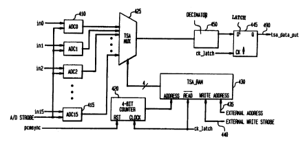
An illustrative embodiment of the apparatus of
the present invention is shown in Figure 4. The
multi-channel device depicted therein is a multi-channel
CODEC which utilizes a shared device 450. For purposes of
illustration, a decimator 450 is the shared device. It
passes data between a number of oversampled
analog-to-digital converters 410 to 415, which in turn
receives inputs in0-inl5. The oversampled converters (not
shown) may use a very low resolution (e.g., 1 bit) to
sample and encode analog signals at a very high sampling
rate. The over-sampled data is decimated to reduce the
effective number of samples of the outgoing PCM data
(tsa-data-out). The decimated data are output directly
onto the TDM bus 490. It can be seen that the
shared-decimator function is output synchronously with
the TDM reset or sync pulse (pcmsync) without buffering
or delay.
9
- 2186918
The operation of the illustrative embodiment
of the invention as shown in Figure 4 is more readily
apparent when viewed in connection with the timing
diagram of Figure 5.
The TDM bus sync pulse (pcmsync) is the
minimum or the slowest clock cycle. The sync pulse
signals the start of a cycle to place the output data on
the TDM bus and for the present illustrative embodiment,
it runs at a 1 MHz rate. The pcmsync pulse is also used
to reset or synchronize the data channels.
For the 16-channel data to output data from
each channel within each TDM bus sync pulse, the channel
data must be output at a speed of 16X the TDM bus data
rate. Thus, the channel data clock (ck-latch) operates
at around 16 Mhz. The ck-latch clock is divided by
counter 420 to provide a 16 Mhz count, which is output
to the address lines of the TSA RAM memory 430. The
output from TSA RAM 430 is used to control the TSA MUX
425.
The TSA RAM 430 stores the channel-to-timeslot
assignment data, which may be input or written from an
external source via the external address 435 and
external write strobe 440 lines. The order in which
data is output from the TSA MUX 425 is controlled by the
channel-to-timeslot assignment data stored in the TSA
RAM. Thus, the channel to timeslot order assignment may
be customized and externally controlled.
During operation, the counter 420 serves as a
pointer to TSA RAM 430 to sequentially cause each
assigned channel to be placed on the TDM bus 490 through
10
'Z186918
latch 445. The data stream output onto the TDM bus 490
is shown in Figure 5 in sequential channel/timeslot
order. However, as explained above, the
channel/timeslot output may be customized in any order
depending upon the channel/timeslot data stored in the
TSA RAM 430.
The sync pulse pcmsync resets the counter 420
to synchronize the above described data selection and
processing.
Conversely, analog signals may be
reconstructed from digital data within each channel of
the CODEC. The data are provided from the TDMB directly
to the interpolation portion of the shared circuit
without buffering or time delay. The data arrive at the
interpolator and is processed in synchronization with
the TDMB bus. This is in lieu of conventional methods,
where data are held back (e.g., within buffers as in the
prior art shown in Figure 3) until the interpolator
detects the "right" phase.
The present invention also envisions a method
for processing data within a shared functional circuit
of a multi-channel device in synchronization with
predefined communications timing. In particular, the
method of this invention envisions receiving and
decimating oversampled bit stream data from each channel
of a multi-channel CODEC. The decimated data from each
channel are processed and output in a synchronized state
with each channel's particular timeslot on a time
division multiplexed bus. Conversely, data provided by
the bus for interpolation (as part of a digital to
2186918
analog conversion process) are transferred in
synchronization with the timing needs of the destination
and/or bus timing to the shared circuit, directly, for
conversion to analog data signals.
S In a preferred form, the present invention
provides a circuit and method for arranging data flow
between multiple channels and a shared functional
circuit within a multi-channel CODEC. Each channel's
data is transferred to/from the shared circuit from/to a
TDMB. Thus, the Group delay typically incurred during
multi-channel, shared functional circuit CODEC
processing is substantially eliminated. The shared
functional circuit preferably performs a
decimator/interpolator function, whereby decimated
channel data are output directly onto the time division
multiplexed bus and data for decoding are provided from
the bus directly onto the shared function. However, in
certain cases, it is desirable to add delay, as when
equalizing transmit time over a transmission path. This
may be accomplished by appropriate choice of timeslot
position in the TSA RAM.
What has been described herein, such as a
method for sharing a decimator/interpolator function
whereby processed data is output in synchronization with
systems timing, is merely illustrative of the
application of the principles of the present invention.
Other arrangements and methods may be implemented by
those skilled in the art without departing from the
spirit of this invention.