Note: Descriptions are shown in the official language in which they were submitted.
,~.: ~ ~ 218 6 9 ~- 2
CARD READ/WRITE APPARATUS
BACKGROUND OF THE INVENTION
Field of the Invention
The present invention relates to a card read/write
apparatus for cards provided with at least an IC memory
region, and more particularly, it relates to improvement in
the contact holder in the card read/write apparatus for
electrically connecting to the IC memory region of such
cards.
Description of the Related Art
Conventionally, in a card read/write apparatus for cards
having an optical data storage region and an IC memory
region, or cards having a plurality of memory or storage
regions such as a magnetic recording region, optical data
storage region and IC memory region, there is provided a
contact holder equipped with contact pins that get access to
and effect electrical connection with the IC memory region of
the card for reading information stored in the IC memory
region and for writing information into the IC memory region.
Such a conventional contact holder is constituted of a
box-type arm which is approximately L-shaped and that rotates
about a shaft, as disclosed in Japanese patent laid-open
publication numbers 5-67250 or 7-152884.
Fig. 15 is a diagrammatic perspective view showing mayor
parts of a conventional card read/write apparatus equipped
with a contact holder as described above.
1
218b942
The card read/write apparatus 1 is constituted of a pair
of guide shafts 3 of different length arranged mutually in
parallel on a main frame 2, a card carriage 4 that moves back
and forth in the X direction along the guide shafts 3, card
feed linear motors 5 that drive the card carriage 4 to move
back and forth along guide shafts 3, an optical head, not
shown, that is arranged above card carriage 4 and that is
moved back and forth in the directions (arrow directions Y)
perpendicular to the carrying directions of the card carriage
4, and a contact holder 8 that makes direct electrical
contact with an IC memory region 6c of a card 6 placed on
card carriage 4.
The card 6 as described above includes both an optical
data storage region 6b and IC memory region.6c on one side
face 6a constituting its upper surface.
The conventional contact holder 8 described above is
constituted of a box-type arm 10 of approximately L-shape,
rotatably supported about a shaft 9, and is provided at its
tip l0a with a plurality of contact pins (so-called IC
contacts) 11 that make electrical contact with the IC memory
region 6c. The rear end lOb of the arm 10 is normally biased
so as to rotate in clockwise direction about shaft 9 by means
of a spring 12, so that arm 10 is normally rotated by a
prescribed angle in the clockwise direction by the biasing
force of the spring 12 so as to separate IC memory region 6c
and contact pins 11, thereby cutting off electrical
connection between the IC memory region 6c and contact pins
11.
2
218 6 9 4~2
When, as shown in Fig. 15, card carriage 4 is moved
along guide shafts 3 towards contact holder 8, its tip 4a
abuts the rear end lOb of arm 10, thereby rotating the arm 10
in the anticlockwise direction about shaft 9 against the
biasing force of spring 12, so that IC memory region 6c and
contact pins 11 are brought into contact, making an
electrical connection. Processing can thereby be performed
to read information stored in IC memory region 6c, or to
write information into IC memory region 6c.
Optical data storage region 6b is scanned by the optical
head, not shown, referred to above, and processing is
performed to read the information stored in the optical data
storage region 6b or to write information into optical data
storage region 6b.
However, with the conventional card read/write apparatus
1 described above, arm 10 of contact holder 8 that approaches
and withdraws from IC memory region 6c, as shown in Fig. 15,
is of a construction arranged outside the region across which
the card carriage 4 runs. With this construction, the total
length of the card read/write apparatus 1 is increased and
reduction in the size of the card read/write apparatus 1
cannot be achieved.
Furthermore, with the conventional contact holder 8,
contact pins 11 were arranged at the tip l0a of arm 10 which
was rotatable about shaft 9, and, in order to effect
electrical contact between contact pins 11 and IC memory
region 6c by rotating the arm 10, all the contact pins 11 and
IC memory region 6c had to be made to approach and contact
3
~ 1 ~ 6 942
each other while maintaining a mutually parallel state.
Consequently, it was difficult to make all the contact pins
11 contact IC memory region 6c with uniform pressure. As a
result, the contact pressure between contact pins 11 and IC
memory region 6c would at some pins be excessive and at other
pins be insufficient, leading to poor contact. Thus, it
could become impossible to perform reading of information
from IC memory region 6c or writing information into IC
memory region 6c.
SUMMARY OF THE INVENTION
Taking into consideration the circumstances described
above, an object of the present invention is to provide a
card read/write apparatus of small size yet possible to
perform processing for reading or writing of information from
or into the IC memory region in a stable manner.
In order to achieve the object referred to above,
according to the present invention, in a card read/write
apparatus for reading or writing information from or into an
IC memory region of a card placed on a card carriage, the
card carriage is formed with an IC exposure opening through
which the IC memory region is exposed when the card is placed
on the card carriage, and there is provided contact means
having contact pins that is projected into or retracted from
the IC exposure aperture while it is maintained in parallel
with the IC memory region of the card so as to make contact
with or move away from the IC memory region which is exposed
through the IC exposure aperture, whereby the contact pins of
4
21 8694 2
The contact holder are made to approach while maintaining a
mutually parallel state of the contact pins and the IC memory
region, with the result that the plurality of contact pins and
the IC memory region are brought into contact with uniform
pressure, thereby enabling reliable electrical connection to
be achieved between the plurality of contact pins and the IC
memory region. Thus, stable processing to read and write
information from or into the IC memory region of the card can
be performed.
In a broad aspect, then, the present invention relates to
a card read/write apparatus having a card carriage driving
means disposed on a main frame of the card read/write
apparatus, and a card carriage which reciprocates along the
main frame by means of the card carriage driving means, for
reading or writing information from or into an IC memory
region of a card placed on the card carriage reciprocating by
means of the card carriage driving means, comprising: an IC
exposure aperture formed in the card carriage, through which
the IC memory region of the card is exposed when the card is
mounted on the card carriage; a contact holder provided on the
main frame in a region where the card carriage reciprocates
exclusive of a region where the card carriage is located, and
having an upper surface on which contact pins are disposed;
and raising and lowering means provided on the main frame, for
raising and lowering the contact holder while maintaining the
contact holder to be in parallel with the IC memory region
when the card carriage stops at a position where the IC
5
r
~' b..: '.. .
2~ 8694 2
exposure aperture contronts the contact holder so that the
contact holder is protruded into or retracted from the IC
exposure aperture, whereby the contact pins are brought into
contact with or move away from the IC memory region.
In other objects and advantages of this invention, it
will be easily appreciated from the following detailed
description and appended drawings.
Fig. 1 illustrates one face of a card used in a card
read/write apparatus according to the present invention;
Fig. 2 illustrates the other face of a card used in the
card read/write apparatus according to the present invention;
Fig. 3 is a perspective diagram of major parts of the
card read/write apparatus according to the present invention;
Fig. 4 is a perspective diagram of major parts of the
card read/write apparatus according to the present invention;
Fig. 5 is a cross-sectional view of major parts showing
the contact means of the present invention;
Fig. 6 is a cross-sectional view along the line V-V of
Fig. 5;
Fig. 7 is a view showing the action of the contact means
of the present invention;
5 (a)
.~. 218 6 9 4-2
Fig. 8 is a cross-sectional view along the line VIII-
VIII of Fig. 7;
Fig. 9 is a view showing the action of contact means
according to the present invention;
Fig. 10 is a cross-sectional view along the line X-X of
Fig. 9;
Fig. 11 is a cross-sectional view of mayor parts
illustrating another embodiment of contact means according to
the present invention;
Fig. 12 is a cross-sectional view along the line XII-XII
of Fig. 11;
Fig. 13 is a view showing the action of another
embodiment of contact means according to the present
invention;
Fig. 14 is a cross-sectional view along the line XIV-XIV
of Fig. 13; and
Fig. 15 is a perspective diagram of mayor parts of a
conventional card read/write apparatus.
DESCRIPTION OF THE PREFERRED EMBODIMENTS
An embodiment of a card read/write apparatus according to
the present invention is described in detail below.
Fig. 1 and Fig. 2 illustrate a view from one side and a
view from the other side of a card 20 used in a card
read/write apparatus according to the present invention.
As shown in Fig. l, an IC memory region 21 constituted by
a thin IC is arranged near the left edge practically in the
middle in the width direction on one side-face 20a of card
6
~ ~ ~ ~ ~ ~.z
20. The upper face of the IC memory region 21 constitutes a
contact face that comes in contact with a plurality of
contact pins, to be described later. A pair of strip-shaped
magnetic recording regions 22, 23 are formed near both side
edges of one side-face 20a.
Convex embossed portions 24 denoted by numerals are
formed between magnetic recording regions 23 and IC memory
region 21.
Furthermore, as shown in Fig. 2, on the other face 20b of
card 20, somewhat lower than the middle, there is formed a
strip-shaped optical data storage region 25 having a
prescribed width.
Reference numeral 26 in Fig. 2 denotes a concealing
member for concealing the back face of IC memory region 21.
A card read/write apparatus 30 whereby information can be
read from IC memory region 21 or information can be written
into IC memory region 21 that is formed on the surface of
card 20 described above will be described in detail with
reference to the drawings.
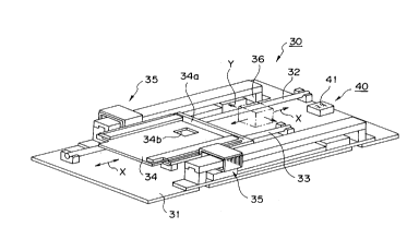
Fig. 3 is a perspective diagram of the mayor parts of the
card read/write apparatus 30 according to the present
invention.
It should be noted that although card read/write
apparatus 30 of the embodiment illustrated below, in actual
use, is employed upside-down, for convenience in description
of the construction, the detailed description thereof will be
given as seen from the same posture as the conventional card
read/write apparatus 1 shown in Fig. 15.
7
~ ~ 8b~~-2
The card read/write apparatus 30 comprises a pair of
guide shafts 32, 33 of different length arranged mutually in
parallel above main frame 31, a card carriage 34 that is free
to be moved back and forth in the directions of arrow X along
these guide shafts 32, 33, card-carriage linear motors 35 for
driving the card carriage 34 back and forth along guide
shafts 32, 33, an optical head 36 arranged above card
carriage 34 and that moves back and forth in the directions
(arrow directions Y) perpendicular to the carrying directions
of the card carriage 34, and a contact means 40 that effects
movement into and out of contact with IC memory region 21 of
the card 20 (Fig. 1, 2) placed on card carriage 34.
Of these components, on the side of tip 34a of card
carriage 34, there is formed an IC exposure aperture 34b
whereby the IC memory region 21 of the card 20 is exposed
when card 20 is placed on the card carriage 34 i.e. when it
is placed on card carriage 34 with IC memory region 21 facing
downwards.
On main frame 31, there is arranged within the moving
range of card carriage 34 a contact means 40 to project into
or be retracted from IC exposure aperture 34b of card
carriage 34.
As shown in Fig. 4, by means of such contact means 40 and
IC exposure aperture 34b, when card carriage 34 is moved
along guide shafts 32, 33 to the location of contact means 40
and is stopped there, the contact means 40 is projected into
or retracted from IC exposure aperture 34b while maintaining
itself in parallel with the contact face of IC memory region.
8
2 i ~b942
Fig. 5 shows a partial cross-section of contact means 40
referred to above, while Fig. 6 shows its cross-section along
line VI-VI. As can be seen from these Figures, contact means
40 comprises a contact holder 42 of rectangular shape in
whose upper surface there are provided a plurality of contact
pins 41, and a raising and lowering means 43 that raises and
lowers the contact holder 42 while maintaining the contact
holder 42 in parallel with the contact face of IC memory
region 21.
Of these components, raising and lowering means 43 is
constituted of a biasing means 44 that biases contact holder
42 downwards, a shaft 45 that extends in parallel with the
contact face of IC memory region 21 and abuts the bottom face
of contact holder 42, and a drive means 46 that drives the
shaft 45 vertically in opposition to biasing means 44 while
maintaining the shaft in parallel with the contact face of IC
memory region 21.
The biasing means 44 is constituted of a pair of guide
shafts 47 erected on the bottom face plate 46 of contact
holder 42 and a pair of coil springs 48 inserted over the
upper ends of the pair of guide shafts 47. The pair of guide
shafts 47 are inserted into a pair of bearing units 42a
projecting from the side of contact holder 42.
Consequently, with the biasing means 44 as described
above, contact holder 42 is normally biased downwards through
bearing units 42a by the biasing force of the pair of coil
springs 48, and is positioned in the initial position shown
in Fig. 5 and 6.
9
Turning now to drive means 46 that effects vertical
movement while maintaining the parallel state of shaft 45
with respect to the contact face of IC memory region 21, as
shown in Fig. 5, the drive means 46 is constituted of a pair
of shaft support members 49 that are free to rotate and
whereon the shaft 45 is mounted in a position offset from the
center of rotation, and a drive motor 51, the tip of whose
rotary shaft 50 is fixed at the center of these shaft support
members 49.
In Figs. 5 and 6, reference numeral 52 indicates a first
position sensor comprising a light emitting element and a
light receiving element, 53 indicates a second position
sensor comprising a light emitting element and a light
receiving element, and 54 indicates a shield plate that
projects at the side of contact holder 42. When the shield
plate 54 shuts off the light path between the elements of
first position sensor 52, it is detected that contact holder
42 is in the initial position in Figs. 5 and 6 and when
shield plate 54 reaches a position in which it shuts off the
light path between the elements of second position sensor 53,
it is detected that contact holder 42 has reached the
prescribed raised position.
Next, the action of raising and lowering means 43 will be
described.
As shown in Fig. 7 (in which the same reference numerals
are used for the same parts as in Figs. 3 to 6), after
loading a card into card carriage 34 with IC memory region 21
being placed at the front and facing downwards, the card
2186842
carriage 34 is made to run towards contact means 40 and is
stopped in a pre-set position i.e. a position in which IC
memory region 21, IC exposure aperture 34b and contact holder
42 are aligned to each other.
After this, when drive motor 51 is actuated, as shown in
Fig. 8, which shows a cross-section along the line VIII-VIII
of Fig. 7, shaft 45 is rotated in the clockwise direction by
means of shaft support members 49 as shown by the arrow C,
while maintaining it in parallel with the contact face of IC
memory region 21.
When this happens, after shaft 45 abuts bottom face 42b
of contact holder 42, the contact holder 42 is moved upwards
against the biasing force of coil spring 48 while maintaining
it in parallel with contact face of IC memory region 21.
Thus, shaft 45 abuts the bottom face 42b of contact
holder 42 and the contact holder 42 is moved upwards against
the biasing force of coil spring 48 while maintaining it in
parallel with the contact face of IC memory region 21.
Thereupon, as shown in Fig. 9 (in which parts which are the
same as Fig. 8 are shown with the same reference numerals)
and in Fig. 10 (which is a cross-section along the line X-X
of Fig. 9), contact pins 41 of contact holder 42 and IC
memory region 21 approach each other while maintaining a
mutually parallel state. The plurality of contact pins 41
and IC memory region 21 are thereby brought into contact with'
uniform pressure, so stable electrical connection can be
achieved between each of the contact pins 41 and IC memory
region 21.
11
2 i 8694-2
Subsequent processing for reading information from the IC
memory region 21 or writing information to IC memory region
21 can then be performed thanks to the stable electrical
connection achieved between contact pins 41 and IC memory
region 21 as described above.
Once the processing for reading information from IC
memory region 21 or writing information to IC memory region
21 described above has been completed, drive motor 51 is
again actuated so that the shaft 45 is rotated by means of
shaft support members 49 while maintaining it in parallel
with the contact face of IC memory 21.
Then, as shown in Fig. 7 and Fig. 8, contact holder 42 is
also moved downwards by the biasing force of coil spring 48
concurrently with shaft 45 and is thereby restored to its
initial position.
In the embodiment described above, raising and lowering
means 43 of contact means 40 is constituted of a biasing
means 44 biasing contact holder 42 in one direction, a shaft
45 abutting the bottom face 42b of contact holder 42, and a
drive means 46 that effects vertical movement of the shaft 45
against biasing means 44 while maintaining the shaft 45 in
parallel with the contact face of IC memory region 21.
However, the present invention is not restricted to this
embodiment. As shown in Fig. 11 (in which parts which are
the same as in Fig. 5 are given the same reference numerals)
and in Fig. 12 (which is a cross-section along the line XII-
XII), a construction is possible wherein the raising and
lowering means 60 of contact means 40 is constituted by a
12
2 i 8 b ~ 4-2
biasing means 61 that biases contact holder 42 in one
direction while maintaining the contact holder 42 in parallel
with the contact face of IC memory region 21 and a link
mechanism 63 supported so as to be freely rotatable about
shaft 62, one end thereof being supported on a shaft 64
passing through the center of bottom face 42b of the contact
holder 42 while its other end is rotated in the clockwise
direction about shaft 62 against the biasing force of biasing
means 61 when it abuts the card carriage 34, whereby the link
mechanism 63 is able to raise contact holder 42 while
maintaining the contact holder 42 in parallel with the
contact face of IC memory region 21.
The biasing means 61 of the raising and lowering means 60
is constituted of a pair of tensile coil springs 66, 67
having the same spring constant, one ends thereof being
engaged with a tongue 65 extending from mainframe 31. Of
these, the other end of one tensile coil spring 66 is engaged
with tip 42c of contact holder 42, while the other end of the
other tensile coil spring 67 is engaged with the rear end 42d
of contact holder 42.
Turning to the link mechanism 63 of raising and lowering
means 60, this is constituted of a pair of L-shaped arms 70
supported on shaft 62, the tip 70a of these arms 70 being
supported on shaft 64 arranged so as to pass through the
center of bottom face 42b of contact holder 42 and the rear
end 70b thereof extends upwards to a position where it is
pushed by tip 34a of card carriage 34 as it runs forwards.
13
21 ~ b g 4-2
The action of raising and lowering means 60 referred to
above will now be described.
With the raising and lowering means 60 as described
above, contact holder 42 is normally pulled downwards by
biasing means 61 comprising the pair of tensile coil springs
66, 67 having the same spring constant and with one ends
respectively engaged with its tip 42c and rear end 42d, and
other ends engaged with tongue 65, so, as shown in Fig. 11
and 12, the contact holder 42 is moved downwards in parallel
to the contact face of IC memory region 21 while maintaining
a balanced condition until it stops in the initial position.
As shown in Fig. 13, in which parts that are the same as
in Fig. 11 are given the same reference numerals, when card
carriage 34 runs in the rightward direction. in the drawing
and its tip 34a abuts the free end 70b of arm 70, arm 70 is
rotated in the clockwise direction as shown by arrow G about
shaft 62.
Thus, when arm 70 rotates in the clockwise direction as
shown by arrow G about shaft 62, its tip 70a is also rotated
in the clockwise direction.
When this happens, contact holder 42 is moved upwards
against the biasing force of biasing means 61 by means of
shaft 64 that is engaged with the tip 70a of arm 70.
However, as contact holder 42 is moved upwards in the
condition of keeping its balance by downwards tension
provided by means of biasing means 61 comprising the pair of
tensile coil springs 66, 67 having the same spring constant
and respectively engaged with tip 42c and rear end 42d
14
2~ ~~~~-~
thereof, contact pins 41 of contact holder 42 and IC memory
region 21 are made to approach each other while being held in
mutually parallel state. As a result, contact pins 41 and IC
memory region 21 abut with uniform pressure, enabling stable
electrical connection between contact pins 41 and IC memory
region 21 to be achieved.
The achievement of stable electrical connection between
the plurality of contact pins 41 and IC memory region 21 as
described above enables subsequent processing to be performed
in which information is read from the IC memory region 21 or
written to IC memory region 21.
When the processing for reading information from IC
memory region 21 or writing information to IC memory region
21 as described above has been completed and card carriage 34
runs in the leftward direction in the Figure, contact holder
42 is moved downwards by the biasing force of biasing means
61 comprising the pair of tensile coil springs 66, 67 and arm
70 is also concurrently restored to its initial position
shown in Fig. 11 by rotating in anticlockwise direction about
shaft 62.
As described above, with the card read/write apparatus of
the present invention, the card carriage is formed with an IC
exposure aperture for exposing the IC memory region of the
card placed on the card carriage, and there is provided
contact means having contact pins. The contact means is so
arranged to move towards and away from the IC memory region
that is exposed from the IC exposure aperture so as to
project into or be retracted from the IC exposure aperture
21 ~69~-2
while being maintained to be in parallel with the IC memory
region. The contact pins of the contact holder and the IC
memory region are therefore brought into proximity while
being maintained in mutually parallel state; abutment between
the contact pins and the IC memory region can thereby be
achieved with uniform pressure; this makes it possible to
achieve a stable electrical connection between the contact
pins and the IC memory region so that processing for reading
information from the IC memory region or writing information
thereto can be performed in stable manner. Furthermore, the
arrangement of the contact means within the running range of
the card carriage such that the contact means can be
projected into or retracted from the IC exposure aperture of
the card carriage enables the overall length of the card
read/write apparatus to be reduced in comparison with the
prior art and thereby enables the card read/write apparatus
to be compact sized.
The present invention can be worked in various modes
without departing from its spirit or main characteristics.
In all respects therefore the embodiments described above are
to be interpreted merely by way of example and not by way of
restriction. The scope of the present invention is defined
by the patent claims and is not restricted in any way by the
text of the specification. Furthermore, all variations or
modifications falling within the equivalent scope of the
claims fall within the scope of the present invention.
16