Note: Descriptions are shown in the official language in which they were submitted.
218704
METHOD TO REDUCE PERCEPTUAL CONTOURING
IN DISPLAY SYSTEMS
BACKGROUND OF THE INVENTIGN
s 1. Field of the Invention
This invention relates to digital video displays, more particularly to
pulse width modulation of data for these displays.
2. Background of the Invention
Binary spatial light modulators typically have elements with two
In states. ON and OFF. When trying to display digital samples of analog data,
this can create come difficulties. The use of pulse width modulation (PVVl~~
allows a relatively true simulation of an analog display, such as a cathode-
ray tube (CRT) based system.
PWM typically comprises dividing the frame time up into segments.
~ s For example, for a system that samples in 8-bit samples, the frame time is
divided u1~ into 255 segments (2~ - 1). The most significant bit (MSB) data is
displayed on a driven element for 128 time segments. If the total binary value
of the pixel associated with that element' has a brightness value of or over
128, the MSB would be a one. This would typically result in the element
2o being ON, where the ON state directs light to the display surface. Other
embodiments will instead turn the element OFF and ON multiple times
within th:U 128 time segments, rather than leave the element in the ON
at.ate for 128 time segments.
t'I-I~1n77 t':~~c I
2187044
The next MSB would then have a time period of G~ time segments, and
so on, such that the next bits would have 32, 1G, 8, 4. '?, and 1 time
segments,
consecutively. The least significant bit (LSB) only has one time segment.. of
which the other times are multiples of, so the smallest time segment is often
s referred t.o as the LSB time. For example, the MSB could be said to have 128
LSB times, rather than 128 time segments.
'rhe LSB can be a limitation on systems using P~VIM. For a color 8-bit
system. for example, each color would have to have 1/3 tb,e frame time. The
frames run at GO l~z. so the frame time is 1/G0, or 1(>.G r milliseconds. For
1 Lhiee color systems (red. green ,;nd blue), each color would only have 5.5G
I1111115PC011(1S. fhe LSB time would then be 21. i ~ I111C1'OSeCOllds.
For most spatial light modulators, this can cause problems. The
switching time of each element must be well under this time. One method
would be to reduce the number of bits per sample. For e~tample, only using 7-
~ s bit samples would increase the amount of time for the L~>B to ~3. i 7
microseconds. However. using less than 8 bits per sample leads to visual
artifacts and contouring. Therefore, a method of~ using PVfM that allows the
use of 8-bit samples within the time constraints of the system and the
modulator is needed.
n-i ni77 f'a;;c _'
2187044
SUMMARY OF THE INVENTION
One aspect of the invention is a method of pulse width modulation for
display data on a spatial light modulator, wherein the data is digitized with
a number , m, bits per sample. A given video frame time is then divided up
s into LSB times for pulse width modulation based upon m-1 bits per sample.
In one frame time, all bits of the m bit samples for the current frame are
displayed using all of the LSB times, except that the LSBs for each sample
are not displayed. In the next frame time, all bits of the m bit samples for
the next frame are displayed, including the LSBs for each sample. This
to frame time has the number of LSB times for the previous frame, plus one
LSB time.
It is an advantage of the invention that it allows the use of higher
numbers of bits to avoid contouring and artifacts in the final displayed
image.
is It is a further advantage of the invention that it does not require a
high transition or switching time of the spatial light modulator elements.
ri-mmo f~:m
2187044
BRIEF DESCRIPTION OF THE DRAWINGS
For a more complete understanding of the present invention and for
further advantages thereof, reference is now made to the follov~ring Detailed
Description taken in conjunction with the accompanying Drawings i1i which:
s FIGURE 1 shows a prior art timing diagram of pulse width modulation
for 8 and 7 bit samples per pixel.
FIGURE 2 shows a flow chart for one embodiment of a method of
alternating frames pulse width modulation for 8 bit samples per pixel.
FIGURE 3 shows a timing diagram for one embodiment of a method of
to altgrnai.ing frame pulse r~~idth modulation for 8 bit samples per pixel.
FIGURE =I shows a block diagram schematic for a circuit to control
alternating frame pulse width modulation for 8 bit samples per pixel.
ri-mm~ r:m~~ a
2187~4~
DETAILED DESCRIPTION OF THE PREFERRED EMBODIMENTS
In Figure 1, a typical pulse width modulation scheme is shown as
timing diagrams for 8 and 7 bits per sample. The number of bits per sample
refers to the number of bits used in sampling the incoming data. Spatial
s light modulators typically display the data for each pixel as a digital
representation. The digital word or sample has a predetermined number of
bits. The higher the number of bits, the more accurate tl-~e digitization, and
the finer the frame time must be divided
Using i bits per sample, which will also be referred to as a 7-bit
to sy~.tem, the least significant bit. (LSB) will be clisplayed for 43.75
microseconds, as shown in Figure 1 on line 10. If one were to refer to the
LSB as bit 0, then bit 1 would be displayed for twice that long, or 2 LSBs.
Bits 2-5 would then have times equal to 4 LSBs, 8 LSBs, 1G LSBs, and 32
LSBs, respectively. The most significant bit (MSB), bit G, would have a time
is equal to G4 LSBs, which is just over half of the available frame time. A 7-
bit,
three color system has 2' - 1, or 127 LSB times. (43. i 4 microseconds times
12 r = 5.5G milliseconds, the frame time for one of three colors in a GO Hz
video system).
The LSB time in a 7-bit system would be manageable for most spatial
20 light modulators, with regard to their transition times between states.
However, .-bit systems have a higher occurrence of artifacts and contouring,
which ciet;rade the picture quality to the viewer. Systems with 8-bits have
hSB firms thm are Z 1. r i microseconds long, as <:an be seen in Figuro 1 on
Tt-~9n77 P.yc
2 i 87044
line 12. This becomes unmanageable when the transitions times of the
modulators are near or even longer than that period of time. However, 8 bits
per sample seems to be the threshold at which the artifacts and contouring
are reduced.
s The dilemma, therefore, exists between the time limitations of the
modulator transition times. and the available time in the GO Hz system.
Figure 2 shows a flow chart for a method which has the advantages of an 8-
bit system, but does not face the disadvantages of such a short LSB time.
In step 20, the number of bits per sample is used to apportion the
1o nuyber of LSB times. The number of LSB times are set as if the number of
bits per sample is the actual number of bits per sample minus one bit. For
example, for an 8-bit system, the apportionment of LSB lames would be done
using 7-bits. The apportionment is done by 2m - 1 LSB times. For an 8-bit
system (m = 8) this would result in 255 LSB times. However, according to
is this embodiment, only m-1 bits would be used, for 2' - 1 or 127 LSB times.
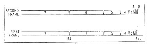
Unce the number of LSB times per frame have been assigned, the data
is displayed in a first frame as if there' were only 7 bits in the system, the
LSB not being displayed, in step 22. In this frame each bit would have the
following number of LSB times: bit 7, Gd; bit G, 32; bit 5, 1G; bit =I, 8; bit
3.
20 4; bit; 2, 2; bit l, 1. This would give a total of 127 LSB times.
In step '?4, the next frame is displayed using the same weighting.
except t.ho L513 is displayed. for 1 I,SI3 tirno. :Vote that in standard pulse
width rnocful;rtion, the L,S13 would Iyt»callv 1o~ displayed for only 1/'? an
f~SB
I I-I')n7? I'a~c c,
2 1 87044
time in the scheme discussed above. In this case, the frame would have 128
LSB times, instead of 127. This extra LSB time could be apportioned in
several ways. For one example, the first frame could be divided up into 128
LSB times, each 43.-10 microseconds long. The last LSB time could just be
s ignored by not displaying any data at all during that time. For another
example, the first frame would remain divided into 127 LSB times, each of
44. 7 7 microseconds. Regardless of how the first frame is divided up, the
second frame would always be divided into 128 LSBs. In the latter example,
the control circuitry would have to be able to adjust to the different frame
to tirr~es. The alternation between frames repeats indefinitely, until the
system
is turned OFF or assumes some other inactive state.
The various values of LSBs and times are shown in the following table.
In the table, the phrase "equal frame time" refers to the first example shown
in Figure 3, and "proportional frame time" refers to the second example.
First Second
Frame Frame
_
Bit LSBs Equal frame Prop. Frame timeL.SBsFrame time
time ( sec) ( sec)
( sec)
7 64 27 7 7. 7 78 2799.650 G4 2778.778
G 32 1388.889 1399.825 32 1388.889
1G 694.4444 699.9125 1G 694.4444
4 8 34 7 .2222 349.9563 8 347.2222
3 4 173.6111 174.9781 4 176.6111
2 2 86.80 5G 8 7.4891 2 86.8056
1 1 43.4028 43. 7445 1 43.4028
- 1 43.=1028 0.00 1 43.4028
Total 128 55~5.;i6 5 55.-1.57 -.____-_. 5555.56
The selection of which method used to accommodate the extra LSB
time in the sc~c;oncl Ii~anro is up to the dosigner. Factors which may
determine
rt-mm~ o:m _
2187044
the selection include: the artifacts and contouring elimination requirements
of a particular system: processing capabilities to control different frame
times; and the speed and performance of the modulator in use.
One example of a possible system architecture that could be used to
s accommodate either of the examples above, among others, is shown in Figure
4. In Figure 4, the spatial light modulator, .10, has an associated memory 42.
The incoming data is processed by formatter -18, which may include sampling
the data at a rate equal to m bits per sample. A sequence controller, 44, will
control the rat.o at which the data is accessed prom the memory and sent to
to the~modulat,or. The sequence controller could be desigmedl or programmed to
either change the length of the LSB times between frames, or just turn OFF
all of the modulator elements for one LSB time.
The sequence controller receives a signal from the goggle circuit 4G,
which is responsible for switching states, or storing a value, that indicates
is whether the next frame has 12 i LSBs of data, or 128. The toggle circuit
would send one of two signals upon the reception of the Frame synch signal.
If the previous signal indicated a I2 i-LSB frame, the current signal would
indicate a 128-LSB frame. Upon reception of the next. frame synch signal,
the signal sent would be reversed accordingly.
2e Tho above method and circuit allows the use of~ 8 hits of data per
samplo to <~voicl the contouring anti artifacts in systems using less than 8
Fits. yet still allows enough time Iur t.hc> st~atiul light modulators to
change
st,~tos witlW o tl~f~ time f.~ramos ;illwvc>ci. 'f lm UisEolav- of the l,SI3
ev~rv other
I I-1'l~n~ t~.i,~~, x
2187044
frame was originally thought to cause a perceptible temporal nonuniformity
between frames. However, in testing, this nonuniformity was undetectable.
Additionally, the display of the LSB only every other frame reduced the
contouring and artifacts that existed in a 7-bit system, or an 8-bit system
s where the LSB was just removed from all frames of data.
Although the discussion has been centered around an 8-bit system
displayed with 7-bit timing, this method can be applied to other cases, such
as a 9-bit system displaying a frame with 8-bit timing. Additionally, more
than one bit can be time modulated in this manner, such as 8-bits displayed
m with G-bit timing. While this last example caused flicker in initial
experiments, a 10-bit system displayed with 8-bit timing did not. In the first
frame, all of the bits would be displayed except the least significant bits.
The
next to least significant bit would be displayed every other frame, and the
least significant bit would be displayed every fourth frame.
~ s Thus, although there has been described to this point particular
embodiments of an alternative method of pulse width modulation, it is not
intended that such specific references be'considered as limitations upon the
scope of this invention except in-so-far as set forth in the following claims.
m-mm~ n:m o