Note: Descriptions are shown in the official language in which they were submitted.
wog5~27920 2 87 156 ~ "o
DISPLAY SCREEN
This invention relates to liquid-crystal displays.
Thin panel screens are available which use liquid
crystal devices, usually of the twisted nematic or
supertwisted nematic type, operating in "Grey Scale" or
passive mode in which orthogonal electrode grids are
used to address individual pixels using multiplexing.
However, their slow speed of operation, measured in
milliseconds, is a major drawback and when passively
multiplexing greater than 100 ways Yiewing angles are
severely restricted for such displays. Moreover
supertwisted nematic displays, being wavelength-
sensitive, show poor black/white contrast.
The use of thin-film transistors, usually referred
to as TFT' s, allows the twisted-nematic effect to be
used at higher multiplexing levels with good contrast.
However it re~Iuires production processes which are both
expensive and difficult to control. Each pixel
requires a TFT and since millions of these may be
needed and only one or two faults are sufficient to
produce an unacceptable display, overall yields of
displays rapidly ~1;m;n; sh as larger pixel arrays are
required. A large, thin, full-colour display panel,
for instance for use in broadcast television, is still
not commercially feasible.
The standard television transmission system i~ the
United Ringdom uses the PAL video system of colour
production. I~ this the frame time for each picture
update is 40 milliseconds (1/25 or .04 sec) and with
625 lines per frame each line is addressed for 64
microseconds (64 ILsecs). Therefore televisions which
use cathode ray tubes with an electron beam scanning
system scan each line in 64 fLsecs. The same line is
re-addressed after a delay of 40 millisecs (frame
time); interlacing of the lines takes place but it is
not necessary to explain the reasons for this for the
.
WO9sl27920 ~ 21 8 156 r~ >5~
purposes of this invention. The final display
currently provided by cathode ray tubes (CRT' s) is
second to none, but CRT' s are of courfie bulky and
power-consu~ing. The invention is an attempt to
5 provide a Iiquid-crystal display which can erqual or
surpass the best CRT's fDr the standard 625-li~e system
and even for the new high-definition screen.
Various designs of LC displays have bee~ : ~
suggested. In many~currert types the liguid crystal is
10 used as a shutter, using either the scattering effect
or its birefringent properties~ to select whether light
from a light source under a given pixel of the LC layer
reaches the viewer. This aLLd~-y~ leads to problems
with viewing angle, since the LC i5 sensitive to the
15 angle at which the light passes through it.
One ~L~ ~1ng approach to dealing with the
viewing-angle problem is to use phosphors for the
visible light emissions; for instance, EP-~.-18~495
(ITT) shows a display unit comprising a W r;3~1; Atinn
20 source which is used to cause E~hn~rhnr elements on a =
screen to glow, wherein the supply of rA~liAtinn to the
phosphor elements is controlled by means of a liquid-
crystal shutter. ~ The back plate, which guides the
light to the LC layer~ is side-lit and the liquid
25 crystal itself operates on the scattering principlel
where the light is rnntA;n~fl within the light guide and
the LC by total ;ntio~nAl r~f1et-t;r,n, until it meets a
LC cell which is activated, whereupon the light is
scattered. Some of the scattered light, namely that
30 proportion which is deflected E~lff;r;~ntly near to the
normal o~ the layers, then passes out of the LC layer
to the corresponding phosphor dot,~ which then glows.
Such devices have the advantage among others that
the light sent to the viewer (the "display" light) is
35 not the ligh~ that has passed through the LC layer (the
"actlvating~ lLght); this fact alone can rnnt~ te
.
Wo 9sl279~0 2 1 8 7 1 ~ 6 r~
--3
- markedly to solving the typical LCD problem of
restricted viewing angle, a problem which is not 301ved
by displays using phosphors or fluorescent materials
lln~ rn~Ath the LC layer, such as that shown in US
5 4167307 (Siemens).
Another approach is described in US 4830469 (~S
Philips). ~Iere a supertwist liquid crystal, i.e. one
having a molecular twist of more than 180, is used.
Such LCs are difficult to use in the conv~ntinn~l way
10 with filters for colour displays, so this display uses
phosphors. The phosphors, instead of being on the
outside of the glass plate which encapsulates the
li~uid-crystal ~layer, are placed directly on the LC
electrodes on one side. Accordingly it is very
15 difficult to incorporate a polariser, and this display
theref ore does away with one or both polarisers and
uses a dichroic W dye instead, which restricts viewing
- angle. Further it is not possible to use standard TN,
STN or erroelectric LCs with the Philips arrangement.
The main features of the system on which the
invention is based are as follows:
A. A plurality of self-rA~l;at;n~ ~l, tc are
used, I l;f;f-~ by materials known as "Phosphors",
forms of which are used in curre~t cathode-ray tubes;
B. The rhnsrhnrs can be caused to emit visible
light by energising them with energy, preferably
monochromatic light in the near ultra-violet;
C. To control the output of radiation from each
pixel, electro-optic shutters are used to restrict the
otherwise free flow of energy passing to the r~;At;n~
material. The shutters are controlled in such a way
that each self-radiating pixel is individually
processed. At any given point in time each pixel point
has individual visible light output characteristics.
The shuttering between the excitation energy
source and the light-radiating material should ideally
WO9s/27~20 ~117156 r~ r~
be applied in such a way that~ the viewed output can be
perceived as a c~nt;nllrlus pro~ression from one output
se5uence to the next at rates which will allow moving
imagery to be seen by the viewer without f licker . This
5 process is usually described ;as modulation.
The invention can use conventional Iiquid-crystal
layers to improve upon current thin screens, making ~
them less costly and more energy-e~ficient, but it also
allows the conception of new display panels using
lO state-of-the-art, microsecond-response-time LCs such as
ferroelectric, distorted-helix or electroclinic
materials .
Different li~uid crystals re~uire individual
modulation approaches; for instance, twisted nematic,
super-twisted nematic, distorted helix and
electroclinic forms can grey-scale, and they also
return to their unwritten state when the voltages are
removed. Ferroelectric materials, on the other hand,
are bi-stable (~r~nPm;CPiveJnon-tr~n~ qR;ve) and
remain written ol:Lce addressed. It is therefore
n~ cPS~ry to provide each typé of liquid crystal with
particular information via the address system which
will enable it to act a ~ ; n~ shutter. For
twisted nematic and super-twisted nematic passive and
active TFT addressing are used. Passive multiplexing
relies on the electro-optic effect r~Ppr~n~in~ to the
RMS of the applied P.C voltages. In the case o~
electroclinic and distorted helix effects the DC
voltage will allow a similar response. This is true
0 analogue modulation . ~ ~
Ferroelectric liquid-crystal effec~s on the other
hand have only on-of f states and thus cannot be
multiplexed in this way. Ferroelectric li~uid crystals
are multiplexed in a binary fashion by using their
35 memory. Domain switching, which involves only
partiall~ switc~ ^rroelec~ric 1 ~u~ c stals su~
2~7~
--5--
that only a part of each plxel 18 swltched, is
po~l hle. This allows a form of greyscale, wlth
memory, to be achleved. Hltherto lt has not been
p.~ hl e to achleve pagglve mulf l rl ~y1 n3 of dlstorted
hellx and electrocllnlc liquld crystals, 80 they have
needed to be multlplexed wlth actlve b~lrrl ~nc~
However it 18 an obJect of the lnventlon to allow such
effects to be passlvely multlplexed.
Accordlng to one aspect of the lnvention there 18
provlded a display screen comprislng: a backing layer
acting as a light gulde for actlvatlng llght; a liguid-
crystal layer containing cells which when sultably
addl :~sed allow llght to pass from the backlng layer
through the cell; and an emlttlng layer contalnlng
rhn~3ph~r-type ol ~ L~ ILL. ~ <li n~ to the cells, for
emlttlng display light when activatlng llght reaches
them; characterlsed by the further provlslon of means
for collimating the activatlng llght towards the
rh~sr~h~r-type ~ L~.
The collimation means can be a slmple physlcal
barrier ln the form of an apertured substrate for the
llquld crystal layer, preventing actlvatlng light from
one LC cell reaching a phosphor in a different cell.
However an optical aL L , t ls IJL ~I t~lL L ~d Thls
could be an array of lenses (or 'lenslets' ), or a
graded-refractlve-lndex layer. Such a layer or array
may alternatlvely or additionally be illLLL~duced or
located between the light guide and the llquld-crystal
modulatlng ~ub~LLc-L~, ~5 rP~ ly when llquid crystal
cells exhlbiting blrf~fr~n~nre are employed, as wlll be
~l~.S~r1 h~l ln greater detall herelnafter.
An example of a collimation device usable in
liguid-crystal displays generally is shown in IBM
T~ .hn1~ 1 n~ re Bulletin Vol. 29, No. ll, April
1987, pp. 4838-9. Here a light-guide plate is ~ 1n~r3
wlth a lenslet plate to dlrect relatlvely well
AMENDED SI~E~T
21~71~6
-5a-
collimated light normally towards the LC cells.
The light source preferably, _ ~P~ a
LLd~ L~L plate, forming the light guide, with edges
into which radiation may be S"rr1 1P-3 from a source such
5 as a discharge lamp, from which the radiation is guided
within the plate. A collimation means can then be
~.
AMEN~D SHEET
~Wo 9sl27920 ; 1 8 7 1 5 6 r~ c / /u
provided by an apertured plate positioned above the
light guide itself, with the liguid crystal material
being provided in each aperture Indentations or
protuberances, forming points from which the r~ t;nn
may be emitted, may be provided alternatively to the
apertures .
As the liquid-crystal-containing layer is very
thin relative to that on which the phosphors are
placed, etching of the phosphor-carrying substrate for
each pixel can be used to bring the phosphor closer to
the modulating liquid crystal.
The thin screen device is a composite structure
designed so that the radiating phosphor used for each
individual emission can be incorporated into the screen
in any preferred position on or within the panel, on
the surface or intP~nA11y.
Ultra-violet light can be introduced into the
panel in one of two ways, either by directly applying
the U.V. source generally to the back of the assembled
panel or to the edge or edges of a transparent
substrate which will act as a light guide. Depending
on which ill~i~in~t;on source is chosen liquid crystal
shutter control can be provided to ef f ect the required
t; nn .
To maximise the input of U.V. light into the
~ t;n~ substrate, when the panel is edge-lit,
provision may be made to bring specular reflections
normal to the apertures or pixels. This can be
achieved through the use of a mirror which directs the
edge lighting in such a manner. Alternatively
scattering of the light can take place either on the
back surface of the panel/screen or through the use of
indentations on the upper surface of light-guide layer.
The indentations are preferably treated, possibly
roughened, to enable scattering to take place.
Incorporation of scattering entities in the cell itself
~ ~8715~
--7--
could also be used.
General backlighting of liquid crystals is an
~Y~ lon~ method of illllm;n~ n when the birefringence
effect is employed. Hitherto, however, edge l i~ht;n~
5 has not been applied to birefringent systems.
However if the light introduced into the panel
through edge ill~lm; n~ m is made to scatter within the
light guide then liquid crystals with birefringent
electro-optic characteristics can be used with edge
10 lighting. Thus side-lit, lightguided panels/screens
using twisted nematic, super-twisted nematic,
f erroelectric and electroclinic liquid crystals are
p,,c,~; hl e .
In embodiments of the invention therefore the
15 liquid-crystal layer on the backing layer can be
sandwiched between two polarizing layers and contain
cells whose bir~frin~nrP can be altered so as to
affect the passage of light from the backing layer
through the cell; and light normalisation means are
20 provided for n~rr~ ing input light towards the cells.
An example of such light normalisation means is
constituted by a roughened in~lont~ n on the surface
of the wave guide for each liquid crystal cell.
There can be no general backlighting of
25 panels/screens when the modulating substrate contains
liquid crystals of the scattering-mode type; however,
they are excellently suited to edge-lit devices. Such
modulating substrates can be provided using the
scattering electro-optic effect in bi-stable
30 ferroelectric liquid crystals. This relies on a short-
AME~OE~ SHEET
WO9~27920 21 8 71 56 r~
--8 --
pitch helix scattering in one memory state andswitching to a clear memory state. If such scattering
types are used, for example bi-stable ferroelectrics,
then the use of polarizers may be completely
eliminated.
In a third aspect the invention provides a display
screen comprising: a light source; a backing layer
acting as a guide for activating light from the light
source; a bi-stable liquid-crystal layer over the
10 source which cnntA;nc cells which when suitably
addressed allow light to pass from the backing layer
through the cell; and an emitting layer cnntAining
phosphor-type elements corresponding to the cells, for
emitting display light when activating light reaches
15 them; in which the addressing of the liquid-crystal
layer causes the liquid crystal layer to switch between
a scattering state and a clear state. This aspect of
the invention makes use of the great speed of bistable
LC devices while making it possible to ~;m;n:lte
20 polarisers.
The ~lim;nAtinn of one polarizer may also be
possible if a dichroic dye is incorporated in the
~ lAtin~ liquid crystal or by using the dichroic
nature of the liquid crystal itsel~ when operating with
25 wavelengths of light provided by the ultra-violet
spectrum (around 300 nAn~ tres) ~iquid crystals do
not absorb significant amounts of visible radiation,
therefore their dichroic nature cannot be used in
panels/screens which operate with input visible light
30 but since in the invention the shuttered light is not
the light emitted to the viewer it is possible to use
U V light
According to a fourth aspect of the invention
there is provided a display screen comprising: a
3~ backing layer acting as a source of activating light; a
bi-stable liquid-crystal layer ~-)ntAin;ng cells which
. .i , . i 1~,IttA;~
WO95/2~9~0 21 87 ~ 56 r~ u
.
g
when suitably addressed allow light to pass from the
backing layer through the cell; a control means for
addressing the cells in turn, with a given address time
for each cell; and an emitting layer C~nt~ln;n~
5 phosphor-type elements corresponding to the cells, for
emitting display light when activating light reaches
them; characterised in that the control means is
adapted to activate the cell for a variable fraction of
the address time, so as to vary the brightness of the
10 corresponding phosphor-type element.
A grey scale is thus achievable even with bistable
LC layers; such ~Cs would be typified by ferroelectric
(FE) liquid crystals but tight-pitch cholesteric ~i.e.
chiral nematic) I,Cs, for instance, behave in the same
15 way if the address voltages are kept within the
hysteresis range The control of the pixels of a
phosphor screen having a plurality of phosphor regions,
a source of radiation and a corr~Rrnn~;n~ plurality of
control means arranged to control the tr~ne~m; esi~n Of
20 r~rl;;lt;~n from the source to the phosphor regions
involves simultaneously addressing each pixel in a
given row to enable only the control means in that row
to operate and simultaneously supplying a binary signal
to the control means which causes the transmission of
25 r~ t; ~m, the duration of the binary signal
det~ n;n;ns the period during which radiation is
allowed to reach the phosphor forming the corresponding
pixel thereby determining the brightness of the pixel.
An alternative method is to let the magnitude of -~
30 the voltage of the signal determine the r~ t;~n which
is allowed to reach the phosphor forming the
- corresponding pixel, thereby ~t~rm;n;ng the brightness
of the pixel
Displays using the present invention allow the
35 possibility of a further multiplexing option since the
natural persise~nce of the phosphors can be llt; l; 7~ to
~ 2187156
-10-
give a new kind of analogue response. The time
available to switch i9 64 ~secs. However, binary
ferroelectric shutters can switch fully much faster
than this. Thus the transmissive state can be present
5 for any period down to the liquid crystal minimum
response time during the 64 ~sec period and a greyscale
can result. By llt;l;~in~ analogue effects the step in
greyscale involved in the lowest level, being that of
the minimum liquid-crystal response time, can be
10 avoided. Thus the preferred effects would be the
electroclinic, distorted helix and domain-switched
f erroelectric ef f ects .
With the ;nf 1llR;~n of ultra-violet light as an
energising source, phosphors as visible light radiators
15 and a pixel address system which will modulate the
excitation energy through greyscale, analogue,
processing, the persistence of the phosphors can be
used to provide a new, mult;r~ rl, thin panel/screen
display ~lt;l;7;ns fa6t analogue liquid-crystal electro-
20 optic effects.
The polarizer and the analy~er are arranged insuch a manner that the natural state of the liquid
crystal is in non-transmissive form. When the pixels
are addressed through multiplexing techniques within
25 the 64 ~sec line time, phosphor elements emit light
with sufficient output such that the eye and therefore
the brain are given the perception of c~nt; nl]; ty . For
a deeper understanding of the invention, some
embodiments will now be described, by way of example
30 only, with reference to the ~l ying drawings in
which:
Figs. lA and lB show the general layout of pixels
in a display panel;
Fig. 2 is a cross-section of a display panel with
35 a continuous liquid-crystal substrate, by way of
illustration of the background of the invention;
hMENDE~ StJEE~
. ~ 2~
Fig. 3 i8 a cross-section of a display panel
representing an embodiment of the invention;
Figs. 4 and 5 show embodiments corr~rnn~l;n~ to
Figs. 2 and 3 but with a liquid-crystal substrate
5 cnnt~in;ng discrete holes;
Fig. 6 shows a further advantageous light guide
and coll ;r-t;n~ lens arrangement;
Fig. 7 shows scattering and rnll;r-t;n~ means,
variations of which can be used to provide ultra-violet
10 light for modulation by any preferred liquid crystal.
Depending on the chosen liquid crystal scattering or
simple reflection may take place on the back surface of
the light guide substrate;
Fig. 8 is a r~n; f; -d view of part of Fig. 9;
Figs. 9 and 10 show further: ' ~ r tq of the
invention .
Fig. 11 shows typical ~ t j nn voltage waveforms
used when addressing ferroelectric liquid crystals;
Figs. 12 and 13 schematically show address
voltages to be used;
Figs. 14 and 15 show aspects of the orientation of
LCs with respect to the polarisers; and
In re3pective figures of the drawings, like
ref erence numerals denote like parts .
The thin panel/screen display will generally be
provided with a matrix of radiating points as shown in
Fig. lA. An individual radiating phosphor dot pixel is
indicated at 11. Each pixel is provided with phosphor
material which emits light in the vi~ible spectrum
after the application of ~ tr~ ultra-violet light.
Fig. lA shows the line and row a~ rdll~ ' for the
radiating points. Indicated at 5 is the panel with its
plurality of phosphor dots. Shown at 7 and 9
respectively are the upper and lower address lines made
of a suitable transparent conductive materials such as
indium tin oxide. The choice o~ a particular line
~UUE~DED S:HEET
WOss/27920 2 1 ~7 ~ 56 ~ "~
--12--
pair, one upper and one lower, will allow the provision
o mo~ l At j nn information to the modulating layer on an
individual pixel basis. ~lthough each pixel point can
be addressed individually at any point in time or in
5 groups if so required, the preferred method uses
simultaneous addressing of all the pixels in a given
row at the same time, every pixel point in the chosen
row being provided with individual modulating
inf ormation .
When the pixel points in a given line, such as
line (1), in Fig. lA are addres6ed the phosphor
persistence allows visible light emission from each
pixel in the row to nnt;nl-~ after the address
information has ceased and subsequent rows on the
panel/screen are being supplied with modulating
information. All pixels can be rA-liAtin~ visible light
during the picture-forming process but each horizontal
line is addressed at different times during the same
period .
The pixels' phosphors are grouped in Red, Blue and
Green triad or unit cell formation as shown in Fig. lB.
Each cell contains one red, one blue and one green
r~;At;n~ rhns~hr~r. Each triad/unit cell, when
supplied with suitable address inf ormation through each
liquid-crystal ' lAti n~ shutter to be described
below, can reproduce all colours in the visible
spectrum .
Figs. 2 to 10 show different configurations of
panel structure; layers 17, 21, 23, 71, 25, 31, 79, 41, ~
30 44 and different colour emitting phosphors 35, 37, 39
are common to each. Layer 17 is the backing layer,
which must be transparent to the light used, preferably
ultra-violet light, and when edge-lit acts as a light
guide. Layer 21 is its reflective surface,
35 conveniently achieved by the deposition of molecular
amounts of reflective material, possibly silver. The
WOgs/27920 2~ 7ll~ P.,l,~,,, s~ u
--13--
next layer, 23, is the polarizer, on which is formed
the liquid crystal lower cell wall 71. Lower address
lines 25 and upper address lines 31 surround the li~uid
crystal layer 29, which is bounded on the upper side by
5 an upper cell wall 79. Layer 44 is the upper
polarizer, or analyzer, and layer 41 is the final outer
layer, which ~ nt71nq the radiating phosphor dots 35,
37 and 39.
In Figs 2 and 3 the continuous liquid-crystal
10 substrate is shown generally at 29 with sections
between the upper and lower address lines in the active
mode given the numeral 43. This substrate may be
around 5 microns thick for a super-twisted nematic
display and around l . 5 to 2 microns for ferroelectric
15 and electroclinic displays. The layers are of course
not shown to scale in t~e drawings. In an actual cell
the glass layers such as 71 and 79 might be 500~L thick.
The setup shown in Fig. 2 corresponds broadly to
that shown in E~P-A-185495 (ITT). It differs in that it
20 uses birefringence, whereas the display shown in that
1rn-~nt use5 liquid crystals of the scattering type
and ~nt~;n~ no polarisers. Operation of the Fig. 2
device is as ~ollows. Ultra-violet light 57 enters the
backing layer 17 at the gide and is ;nt~rn~lly
25 ref~lected at the front and rear surfaces. The
reilecting grid 21 ensures that the W light can only
enter a cell at the pixel point. The LC material
normally rotates the polarisation of light emerging
from the backing layer 17 via the polariser 23, so that
3 0 it is stopped by the analyzer 44 and the cell appears
dark. When a cell of the liquid-crystal matrix is
- activated it ceases to rotate the transmitted light,
and as a result the ultra-violet light impinging on
that part of the LC layer reaches the phosphor dot 3 5,
35 37, 39, which then emits light of the appropriate
colour .
. I ! ~ .
21 871 5~
-14--
It is important that crosstalk is eliminated in
such a display. This is achieved to a certain extent
in Fig. 2 by the grid of apertures in the reflective
layer 21 which direct the light to the individual
5 cells. For a more ~Lulluullc~d effect, in the embodiment
of the invention shown in Fig. 3, the upper surface of
the backing layer 17 has curved eruptions or
protuberances 47 which act as I~nll ;r-t;n~ lenses.
"Collimation" ib understood here in a loose sense as
10 meaning the directiûn or collection of light to a more
or less parallel normal direction towards the
phosphors. Where cells have birefringence which can be
altered 80 as to affect the passage of light
therethrough, col l; r'ted light needs to enter the
15 cells . Edge l; ~ht i n~ will require not merely
collimation of light before it enters the cells, but
directing of light towards c~ t; ~n means . Such re-
direction is termed Rnorm-l;~t;~n" herein. With
bistable liquid crystals, scattered light emerging from
20 the cells will require collimation or focusing, as
aforesaid, towards the phosphors. These optical
features will become clearer from the description which
f ollows .
Thus, reverting to Fig. 3, ultra-violet light is
25 fed into the layer 17 either gener~lly through the back
surface, 19, indicated at 61, or at its edge or edges,
20, indicated at 57. This light either passes directly
through the polarizer 23, or is first reflected back
into the body of layer 17 by the reflective layer 21
30 and passes through the polarizer after being thus
scattered in the manner previously described.
The eruptions maximise the capture of provided
ultra-violet light before it passes through the
modulating substrate ~-~n~;l;n;ng liquid-crystal
35 material. The spaces between the eruptions are filled
AMENDED SHEET
Wo9s/27920 ~ ~ 8~ r~ v
-15--
with reflective material such as silver. The ultra-
violet light, 75 is shown undergoing collimation by the
aforementioned eruptions, 47, on the surface of the
lightguide substrate, indicated at 17. One ray,
5 indicated at 73, is shown in the body of this
substrate. The lens formed by the eruption 47
effectively collects U.V. light from the substrate
layer 17, directing it towards the pixel; this
increases efficiency and reduces crosstalk.
Figs. 4 and 5 show an alternative way of reducing
crosstalk. The method of ultra-violet light provision
is the same as that previously described. In the
configuration shown the liquid-crystal l~t;nrJ
material is held in discrete holes, indicated at 49,
provided in an opaque substrate 51 such as polymeric
material. Similarly the configuration shown in Fig. 5
holds the modulating liquid- crystal material in the
same way, in combination with lenses 47 as in Fig. 3.
This effectively co1l ;r-tf~ or directs the light to the
respective phosphor.
Fig. 6 shows a further way of increasing the
directionality of the U.V. light. Here substrate layer
surfaces etched at 81 lln~rn~th each of the cells
cause scattering of ultra-violet light; elsewhere a
reflective layer 21 is applied. The preparation is
constituted by an etched depression 25; there is a
similar etching 77 on the lower surface of the glass
outer layer 41. Further lensing may be provided at 97
if required.
Fig. 7 shows a further development using a lenslet
array, shown at 87. Such an array is provided to
collimate the ultra-violet light scattered by the
prepared surface 81, ;nrl~ ;nr the etched indentations
85, or alternatively by the prepared surface 95. Here
the collimation all takes place lln~l~rn~th the ~C
layer. Specular reflections within the lightguide can
W09~/27920 21 8 7156 r~ s~
--16 -
be brought s~lhst~n~;~lly normaI to the apertures/pixels
by the inclusion o~ a mirror 93 behind the ~ lmln~ting
means 86, if required
Fig . 8 shows the collimatlng ef f ect of the lenslet
5 array, 87, for scattered IJ.V Iight 86 provided via
lightguide 17. The shown lenses, 87, can be replaced
by an array which achieves the same effect via a grade~ ~
ref ractive index system.
The invention can also be applied tD liquid
10 crystals exhibiting the electroclinic ef_ect. With
such an effect the optlc axis lies in the plane o~ the
liquid crystal layer. It rotates in this plane to an_
extent proportional to the applied voltage, the
direction changing with its sign. The maximum
15 switching angle pogsible depends on the liquid-crystal
material available It i5 presently about 22 . 5
degrees, so that a voltage change f rom + to - can
produce a maximum change of 45 degrees.
Fig . 9 shows a varied f orm of the panel such as
2 0 can be used in any of the preceding embodiments . On
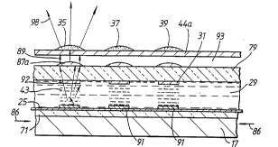
the lower address line 25 a reflective material 91 has
been ~ ros;tp~ in areas corrl~p~ ;n~ to each cell, or
part of each cell. The purpose of this is to prevent
light having entered the ~C layer from being scattered
25 back into the light guide layer, so i~creasing the
forward transmission of energy represented by
backscattered rays 92 travelling to a lenslet array 87a
which unlike that in Fig. 7 is above the ~C layer.
A:Eter crossing a gap 93 typically ct~nt~L;n;ns air the W ~~
30 light causes the ~phosphors 35, ~37, 39 located on the
glass backing ~olate 44a to glow at 95.
Fig. 10 represents an architecture of the: =.
scattering ty~oe similar to that shown in Fig. 9 where
the IJV light is scattered in the liquid-crystal layer~
35 29, sandwiched between two glass layers 71 and 79, and
oDlv colli~ted ~ft~rwa=~ o~r~ h~ phos~h~ ~ 3s-
W09sl27920 2 1 87 1 56 P~ u
--17-
3 9 . The light emerges f rom the sources 8 6 and
propagates within the backing layer~ 17 . From cells in
the non-scattering state light is totally int~rnAlly
re1ected, as shown at 101. At activated cells light
5 102 i3 scattered and some of it proceeds to the lenslet
array 87a. In Fig. 10. 105 represents an LC cell edge
seal and 106 an air gap seal.
The liquid crystal can advantageously be a
f erroelectric LC . A disadvantage of such is that they
10 are bistable, so that varying the applied voltage does
not produce the desired grey scale. The invention
caters for this need by varying the activation time
during the address cycle. Fig. 11 shows the principle.
In (a) the full 64,Ls line time is used, in (b) only a
15 part of it and in (c) again only a part, but divided
into separate sections. The FE LC is thus addressed
only part of the available time; the phn5rhr~r
integrates the amount of light passing and glows with a
corr~Rr-~n-ii n~, nearly constant, brightness to give a
20 grey scale.
Fig. 12 illustrates the addressing of an array of
pixels a line at a time. The strobe voltage Vs
det~rminPc which row is being addressed and the voltage
applied to the columns is between -Vd and +Vd (the data
25 voltage). -Vd applies the maximum voltage to the pixel
and +Vd the minimum.
Flg. 13 shows that if Vs = 2xVd t~is m~l~imi Cl~c the
voltage applied to the pixel, namely Vs + Vd, the
"select~ voltage, compared with the voltage applied to
30 the other pixels whilst their row is being addressed,
namely the "unselect" voltage Vs-Vd, the error voltage
appearing on all other pixels ( + or - Vd) .
The voltage on rows of pixels not being currently
addressed does not fall to zero but to 1/3 the '~select~
35 voltage. This will cause a general illllmin~tir~n of the
screen to an ex~ent that depends on the optical
WO gs/2~920 2 l a 7 1 5 6 r~
response of the.liriuid crystal to voltage (which is
known to be superlinear, thereby reducing the efect),
and the response of the phosphor to U . V . light .
Fig. 14 shows an aLLCL-l~. t for the polarizer and
analyzer so that_ the ~ of f ~ sta~e of the liriuid crysta1
(no voltage~ would give zero light transmission. With
this arrangement +V and -V result in identical optical
transmissions. This allows a symmetrical bipo1ar pulse
(Flg. 15) to be used for each of the waveforms Vd and
VB. I~ this is done ~he waveforms experienced by the
liriuid crystal contain net zero DC component. ~rhis ifi
advantageous because it extends the li~e of the lir~uid
crystal - all conv~ntirn~l liS~uid-crystal devices
arrange the electrical drive waveforms to achieve net
zero DC.
Maximum optical transmission can be achieved, as
shown in Fig. 13 (d), by aligning the polarizer with the
orientatiorl o~ the optic axis of the liriuid crystal
with -V applied_(i.e. -22.5 degrees). The analyzer
remains at right angles to the polarizer. This
~LLd~ t gives the maximum '~on" state transmission
but it does not allow net ZerQ DC to be appIied to the
pixels . In addition the optical tr~nr~ qs; r~n of pixels
on rows not currently being addressed is much higher.
The optimum addressing scheme is one which is a
trade-ofi between the "on" state tr~n~-;.qRion on the--
one hand and voltage rl;Rf-r;m;n~tion on the other.
The principles discussed above could be used with
any LCD r~n~l tl~t can modulate tJ.V. light, such as
twisted nematic and super-twisted nematic devices
providing variable tr~nr~; Rqi r~,~ (analogue) shutters .
The principles can also Qe used with scattering devices
such as sme~tic A, ferroelectric in scattering mode and
short pitch cholesteric . The~ super-t~isted nematic
electro-optic effect offers the highest level of
multipl~; h; 1 ' ty and there~ore appear~ to be the mos=
WOgsl27920 21 87 1 56 r~
--19--
appropriate. Super-twisted nematic devices do not
shutter the whole visible spectrum equally. The
;17l1m;n~tion method described may render this
unimportant and it may be possible to optimise the
5 super-twisted nematic effect for shorter-wavelength
U.V. radiation.
The persistence of the phosphor ;n~ d in the
described invention will allow the electroclinic effect
to be multiplexed offering a new kind of analogue,
lO colour, li~uid-crystal display. Thin Hlgh-Definition
Television displays are also possible using the
described invention as the modulator/switching shutter
speeds used, together with the phosphor persistence,
can operate at the faster scan rates implicit in such
15 devices.