Note: Descriptions are shown in the official language in which they were submitted.
CA 02187354 2005-09-14
1
SEMICONDUCTOR DEVICES AND METHODS
FIELD OF THE INVENTION
This invention relates to the semiconductor devices and,
more particularly, to methods of making semiconductor devices
using III-V semiconductor materials, and to devices made using
such methods. This invention was made with U.S. Government
support under DAAL03-92-G-0264 awarded by the Department of
the Army, and ECD 89-43166 and DMR 89-20538 awarded by the
National Science Foundation. The U.S. Government has certain
rights in this invention.
BACKGROUND OF THE INVENTION
Semiconductor devices, for example, transistors, light
emitters and detectors, fabricated using III-V semiconductor
materials, have become scientifically and commercially
important because of properties such as high speed, low loss,
low noise operation, and relatively efficient generation and
detection of light. For example, III-V light-emitting diodes
and laser diodes are sold commercially for various
applications.
So-called catastrophic optical damage (COD) and power
saturation resulting from junction heating have long limited
the maximum output powers available from semiconductor lasers
[see C.H. Henry et al., "Catastrophic Damage of Laser
Material", J. Appl. Phys. 50, 3721 (1979)]. To alleviate
these effects, a variety of different "window" lasers with
higher COD levels have been successfully fabricated. The
windows can serve to prevent damaging current levels at or
near the laser facets (cleaves). These include non-absorbing
windows formed by both Zn and Si impurity induced layer
disordering (IILD) [see Y. Suzuki et al., "Fabrication of
GaAlAs 'Window Stripe' Multi-Quantum Well Heterostructure
Lasers Utilizing Zn Diffusion Induced Alloying", Electron.
Lett. 20, 383 (1984) R.L. Thornton et al., "High Power (2.1
W) 10-Stripe AlGaAs Laser Arrays With Si Disordered Facet
Windows", Appl. Phys. Lett. 49, 1572 (1986); W.D. Laidig et
CA 02187354 2005-09-14
2
al., "Disorder of An AlAs-GaAs Superlattice By Impurity
Diffusion", Appl. Phys. Lett. 38, 776 (1981); and D.G. Deppe
and N. Holonyak, Jr., "Impurity Diffusion and Layer
Interdiffusion in AlxGa1-xAs-GaAs Heterostructures", J. Appl.
Phys. 64, R93 (1988)], or by etching and crystal regrowth [see
J. Unger et al., "High Power GaAlAs Window Lasers", Electron.
Lett. 22, 279 (1986)]. Zn disordered windows typically suffer
from significant free carrier absorption in the active layer.
Windows formed by Si IILD or by etching and crystal regrowth
are limited more by scattering losses near the window
transition region, resulting in increased laser thresholds and
decreased efficiencies. Smaller improvements in the COD level
have also been demonstrated with absorbing current blocking
windows [see T. Shibutani et al., "A Novel High-Power
Structure with Current-Blocked Regions Near Cavity Facets", J.
Quantum Electron. QE-23, 760 (1987)]. In all of the above
cases, the window regions are defined by planar or non-planar
processing (of varying complexity), followed by cleaving of
laser bars near the center of the window regions. This
necessarily results in windows of varying length that are
large enough to cleave easily.
It is among the objects of the present invention to
improve fabrication of III-V semiconductor light emitting
devices and other devices to facilitate their fabrication, and
to obtain devices having improved operating characteristics
and improved reliability and life.
In the fabrication of III-V semiconductor devices, it is
typical to deposit layers on a substrate to form a structure
of relatively large surface area (sometimes called a
"crystal") that is processed and is separated, such as by
cleaving and/or sawing and/or etching, into many individual
devices, or groups of devices, of relatively small area.
[These may sometimes remain on a common base. ] Applicant has
found that the separating of the crystal, and/or other
processing operations, can result in microscopic cracks and
other structural defects that have a deleterious effect on
ultimate operation of the devices being fabricated.
CA 02187354 2005-09-14
3
It is also among the objects of the present invention to
improve fabrication of III-V semiconductor devices to minimize
the effects of structural defects.
SUMMARY OF THE INVENTION
The present invention relates to improved techniques and
devices employing, inter alia, an aluminum-bearing III-V
semiconductor material and a native oxide of aluminum that is
formed in the semiconductor material.
In the U. S. Patent No. 5, 262, 360 of N. Holonyak, Jr. and
J. Dallesasse, assigned to the same assignee as the assignee
of the present application, there is disclosed a technique of
forming a high quality, stable, and compact native oxide layer
from an aluminum-bearing Group III-V semiconductor material.
[Reference can also be made to Dallesasse et al.,
"Hydrolization Oxidation Of AlXGa1-XAs-AlAs-GaAs Quantum Well
Heterostructures And Superlattices", Appl. Phys. Lett. 57
(26), 2844-6, 24 December 1990: Dallesasse et al., "Native-
Oxide Stripe-Geometry AlXGai-XAs-GaAs Quantum Well
Heterostructure Lasers", Appl. Phys. Lett. 58 (4), 394-396, 28
January 1991 Dallesasse et al., "Native-Oxide-Defined
Coupled-Stripe AlxGa1-XAs-GaAs Quantum Well Heterostructure
Lasers", Appl. Phys. Lett. 58 (8), 834-836, 25 February 1991
and Sugg et al., "Native Oxide Stabilization of AlAs-GaAs
Heterostructures", Appl. Phys. Lett 58 (11), 1199-1201, 18
March 1991.] The technique comprises exposing an aluminum-
bearing Group III-V semiconductor material to a water-
containing environment and a temperature of at least about
375~C to convert at least a portion of the aluminum-bearing
Group III-V semiconductor material to a native oxide. The
thickness of said native oxide formed thereby is substantially
the same as or less than the thickness of that portion of said
aluminum-bearing III-V semiconductor material converted into
the native oxide. The native oxide layer thus grown is more
stable than oxide layers formed from previous methods,
meaning, for example, that they do not degrade under
conditions of normal use and atmospheric exposure. Further,
CA 02187354 2005-09-14
4
the native oxide was demonstrated to . exhibit improved
operating and performance characteristics, for example with
regard to metallization adherence and dielectric properties.
The native oxides were described as being useful in lasers,
transistors, capacitors, waveguides and in other electrical
and opto-electrical devices. Anhydrous oxides of aluminum
were noted to exhibit a relatively low index of refraction
(less than about 2.0) and index of refraction can be used to
distinguish the anhydrous oxide forms from the higher index
hydrated oxide forms that are generally unsuitable for
semiconductor applications due to properties such as expansion
and instability.
Applicant has discovered that by implementing oxidation
to obtain a native oxide of aluminum after a device (or
devices) has been metallized (and device fabrication would
normally be complete or virtually complete), advantages can be
obtained in device operation, reliability, and life. In
addition to the advantages that will be shown to accrue from
selectively oxidizing relatively higher aluminum composition
material in the device after fabrication is almost complete,
the oxidation-after-metallization hereof also provides a
sealing effect on the device, acting to seal cracks and other
defects which are present in the processed device. Not only
does the formation of insulating native oxide material in
cracks and defects minimize undesirable carrier flow at such
defects, but a degenerative effect, whereby such current leads
to still further damage, is reduced or eliminated. Also, the
presence of the resultant relatively stable native oxide in
these defects reduces or eliminates the deleterious longer
term oxidation (hydrolyzation), which can lead to
deterioration of the device.
In accordance with an embodiment of the invention there
is disclosed a method of making a semiconductor device,
comprising the following steps: forming a structure
comprising layers of III-V semiconductor material, at least
one of said layers being an aluminum-bearing III-V
semiconductor material; applying metal electrodes to said
CA 02187354 2005-09-14
structure to form a metallized semiconductor structure; and
heating said metallized structure in a water-containing
environment to convert a portion of the aluminum-bearing III-V
semiconductor material to a native oxide of aluminum. [As
5 used herein, metal electrodes and metallization includes
electrically conductive metals and materials containing such
conductive metals.] In a preferred embodiment of the
invention, the heating step comprises heating to a temperature
of at least 375~C in an environment which comprises an inert
gas and water vapor. The heating is preferably to a
temperature that is less than a temperature at which said
electrodes would deform. In most, but not all, cases, heating
will be to a temperature that is less than 550 C.
In accordance with a further form of the invention, a
method is set forth for making a semiconductor laser device,
comprising the following steps: a) depositing successive
layers of III-V semiconductor material to obtain a lower
confining region, an active region, and an upper confining
region, at least one of said confining regions including a
layer of aluminum-bearing III-V semiconductor material; b)
applying upper and lower metallizations to the structure
obtained in step (a), said upper metallization including a
plurality of stripes in contact with the structure obtained in
step (a); c) cleaving the structure obtained in step (b)
across said stripes; and d) heating the metallized structure
in a water-containing environment to convert a portion of the
aluminum-bearing III-V semiconductor material to native oxide
of aluminum. In an embodiment of this form of the invention,
at least one of the confining regions is formed by depositing
layers of aluminum-bearing III-V semiconductor material having
different aluminum fractions. In this embodiment, the layers
of aluminum-bearing III-V semiconductor material are aluminum
gallium arsenide, and the heating step comprises heating for a
time sufficient to form a lateral oxide spike in the higher
aluminum fraction layer.
Further features and advantages of the invention will
become more readily apparent from the following detailed
CA 02187354 2005-09-14
description when taken in conjunction with the accompanying
drawings.
BRIEF DESCRIPTION OF THE DRAWINGS
Fig.~l is a photograph of the surface of a cleaved AlXGa1_
xAs-GaAs-InyGal-xAs QWH crystal after "wet" oxidation (425~C,
lh). The buried oxide forms anisotropically, starting at the
exposed edges of an Alo,9Gao.iAs layer and proceeding laterally
into the crystal. The edges occur along the (110) cleave and
along cracks at the surface of the crystal. Arrows are used
to delineate the oxidized regions.
Fig. 2 is a photograph (top view) of the (110) cleaved
edge of an AlXGa1-XAs-GaAs-InyGal-yAs QWH (a) as-grown, (b)
oxidized (425~C, lh), and (c) oxidized (425~C, 2h). The oxide
extends ~3.5 um into the crystal in (b), and ~7 um into the
crystal for the longer oxidation time of (c).
Fig. 3 is a scanning electron microscope (SEM) image of a
stained cross section of a QWH crystal that is edge-oxidized
from a cleaved surface (425~C, 2h). The oxidation consumes
~7.5 um of the exposed Alo.9Gao.~As layer as the reaction
proceeds laterally (to the left) into the crystal. The oxide
spike widens near the cleave edge as the surrounding
Alo.~Gao,3As layers begin to oxidize.
Fig. 4 shows continuous 300 K L-I curves for oxide-window
AlXGa1-XAs-GaAs-InyGai-YAs QWH lasers ( see Fig . 3 ) with ( a ) no
windows, (b) -4-um-long windows, and (c) ~7.5-pm-long windows.
The longer windows effectively reduce the heating at the
laser facets, resulting in increased maximum output powers.
For reference, the inset shows the longitudinal mode spectra
of a non-window device below threshold (15 mA) and above
threshold (25 mA) .
Fig. 5 is simplified cross-sectional view of the laser
device described in conjunction with Figure 1-4, and
fabricated in accordance with an embodiment of the method of
the invention.
Fig. 6 is a simplified cross-sectional view of a light-
emitting diode device that can be fabricated in accordance
CA 02187354 2005-09-14
7
with an embodiment of the method of the invention.
Fig. 7 is a simplified cross-sectional view of a
transistor device that can be fabricated in accordance with an
embodiment of the method of the invention.
DETAILED DESCRIPTION
In an example of an embodiment hereof, a quantum well
heterostructure crystal is grown by low-pressure metalorganic
chemical vapor deposition (MOCVD) [see R.D. Dupius et al.,
"Preparation And Properties Of Gal-xAlXAs-GaAs Heterojunctions
Grown By Metallorganic Chemical Vapour Desposition", in
Proceedings of the International Symposium on GaAs and Related
Compounds, edited by C.M. Wolfe (Institute of Physics, London,
1979), pp. 1-9: M.J. Ludowise, "Metalorganic Chemical Vapor
Deposition Of III-V Semiconductors", J. Appl. Phys. 58, R31
(1985)). on (100) n-type GaAs substrates in a modified Emcore
GS 3000 reactor. The growth pressure is ~90 Torr and the
growth temperature is 760~C. The dopant sources used are Si2Hs
and CC19. A ~0.1 um n-type GaAs buffer layer is grown first,
followed by an n-type composite lower confining layer of ~0.5
~Zm Alo.7Gao,3As and ~0.5 um Alo.aGao,sAs. A 2000 Angstrom
waveguide region is grown next, and has a 75 Angstrom strained
layer of InyGal-yAs (A of about 960 nm) quantum well centered in
960 Angstroms of GaAs, which is further confined by 480
Angstroms of Alo.lsGao.asAs on either side. The p-type upper
confining layer consists of first ~0.5 um of Alo,4Gao.sAs and
then -1000 Angstrom of Alo_9Gao,lAs (the layer for subsequent
oxidation) sandwiched inside a pair of 1500 Angstrom
Alo,7Gao.sAs layers. Finally, a 1000 Angstrom p-type GaAs
capping layer is grown that includes a heavily carbon-doped
contact layer grown at 550~C.
In the present example, laser fabrication begins with the
patterning of ~12 um-wide photoresist stripes on the crystal
surface. The stripes mask mesa etching (1:8:160,
HZS04 : H202: H20, 2 . 5 min) that removes all but 1500 Angstrom of
the p-type upper confining layer outside the stripes,
resulting in 10.5 um-wide ridges. The photoresist is then
CA 02187354 2005-09-14
removed, and a Si3N4 layer is deposited over the entire crystal
by chemical vapor deposition at 700°C. Another
photolithographic step and CFQ plasma etching are used to
define ~4 pm contact openings in the Si3Na centered on the 10.5
um ridges. After the photoresist is again removed, the
crystal is lapped to 100 um and polished. The n-side
metallization is performed next, and consists of a Ge-Ag-In
alloy (600°C, lOs), followed by the Ti-Pt-Au p-side
metallization. The crystal is then cleaved into bars 0500
um-long cavities) that are ready for oxidation.
Some of the metallized bars are placed in an oxidation
furnace (425°C) that is supplied with a H20-vapor saturated N2
flow. Also, samples of unprocessed crystal (bare surface)
with freshly cleaved edges are simultaneously placed in the
oxidation furnace to provide comparison samples. A photograph
of the surface of the unprocessed crystal after oxidation at
425°C for lh is shown in Fig. 1. The right side of the
photograph shows the rough scribe mark used to initiate the
crystal cleaving. One part of the scribe mark causes a crack
to propagate along the crystal surface (diagonally to the
left) before reaching the (110) cleave edge. In the regions
where high composition AlXGai-XAs is exposed, i . a . , along
the scribe mark, along cracks, and along the cleaved edge, the
AlXGa1-XAs is converted to a high-quality insulating native
oxide as shown in the top view of Fig, 1. The oxidation is
anisotropic, preferentially "consuming" the Alo.9Gao.iAs layer
near the crystal edges (as well as cracks and crevices) and
proceeding -4 ~zm laterally under the lower composition cap
layers. The extent of the oxide is visible from the crystal
surface since the low index (n~1.63) of the native oxide makes
the oxidized regions more reflective than the rest of the
crystal. The GaAs cap layer provides an effective mask for
surface oxidation at 425°C [see J.M. Dallesasse et al.,
"Native-Oxide Stripe-Geometry AlXGai-XAs-GaAs Quantum Well
Heterostructure Lasers", Appl. Phys. Lett. 58, 394 (1991)].
As is evident in Fig. 1, the oxide tends to electrically
CA 02187354 2005-09-14
9
isolate small cracks ("Ox" label - visible in original) that
are barely visible on the crystal surface. Thus, the oxide
forms a seal or "guard ring" that tends to block current
injection from damaged areas of the crystal.
The oxidation conditions control the amount (extent) of
electrical isolation near cleaved (110) edges. Three
photographs of the QWH crystal surface are compared in Fig. 2.
The (a) photograph shows a cleaved edge of the as-grown
crystal, while the (b) and (c) photographs are of samples
(unprocessed crystals) that are cleaved and oxidized at 425°C
for 1 and 2 hours, respectively. The laterally grown oxide
extends (b) ~3.5 and (c) ~7 um from the (110) cleave edge into
the crystal. For longer oxidation times, the anisotropic
oxide layer thickens near the cleave edge as the Alo.7Gao,3As
layers surrounding the Alo.sGao.iAs layer begin to oxidize.
This is evident in Fig. 2 (c) as a darkening adjacent to the
(110) edge.
A scanning electron microscope (SEM) image of a stained
crystal cross section is shown in Fig. 3. An unprocessed QWH
crystal is cleaved and laterally oxidized (425°C, 2h). The
resulting oxide shown in Fig. 3 is ~7.5 um long and varies
continuously in thickness from 0.45 um at the (110) cleave
edge to 1000 ~1 at the tip of the oxide spike. The
anisotropic nature of the oxidation results in rapid oxidation
of the thin (1000 ~) Alo.9Gao.iAs layer, and more gradual
oxidation of the surrounding Alo.7Gao,3As layers . Both the
waveguide and surrounding Alo.4Gao,6As layers remain essentially
unoxidized since they are of lower aluminum composition. The
bright line that appears to the left of the oxide spike in
Fig. 3 is an artifact of staining.
The metallized bars are assumed to oxidize exactly like
the comparison samples presented in Figs. 1-3, since the
initial conditions (freshly cleaved edges) and the oxidation
times and temperatures are held constant. Also, Applicant's
experience with actual cross sections shows no differences in
the oxidation behavior of metallized and non-metallized
specimens. The oxidation temperature is low enough to avoid
CA 02187354 2005-09-14
melting or re-alloying of the metallizations.
Light vs. current (L-I) characteristics (pulsed
' excitation, 1$ duty cycle) of the metallized AlXGai-XAs-GaAs
InyGal-yAs QWH laser diodes are measured prior to "window"
5 oxidation. On each bar individual devices are isolated by
shallow saw cuts. Typical threshold currents for these 10.5-
um-wide ridge-waveguide devices are ~25 mA for 500-um-long
cavities. After the oxidation procedure that forms the
current-blocking facet windows, the L-I characteristics of
10 each diode are measured again. For bars that are oxidized at
425~C for lh (~4-um-long windows), the threshold currents
typically increase by ~0.5 mA. Threshold currents of bars
oxidized at 425~C for 2h (~7.5-um-long windows) or at 450~C for
45 min (~6.5-um-long windows) increase by ~1.5 mA. The
differential quantum efficiency remains almost unchanged after
all oxidations. Losses in the unpumped window regions cause
the slightly larger pulsed threshold currents of the oxidized
laser bars. The current-voltage (I-V) characteristics are
unaffected by the oxidation process. The series resistance of
the diodes is about 3 ohms.
After the window oxidations are complete, the laser bars
are diced and the individual diodes are mounted p-side down on
In-coated copper heat sinks for continuous wave (cw)
operation. Six comparison non-window diodes (from four
different unoxidized bars) axe also mounted. All of the non-
window devices are driven cw until burn out by COD. The power
at which COD occurs varies from 150 to 192 mw/facet for
uncoated non-window lasers. The L-I characteristic (cw 300 K)
of the best (highest power) non-window device tested is shown
in Fig. 4 (a) . This device fails by COD (192 mw/facet) at a
current of 580 mA (10.5 kA/cm2).
A typical L-I characteristic for an oxide-window (~4 um-
long window) device is shown in Fig. 4 (b). Before COD
occurs, these devices typically operate to 190 mw/facet, a
power equal to that of the best non-window devices. However,
the devices with 4 um-long windows do not fail abruptly at
this power. Instead, heating causes the L-I curve to bend,
CA 02187354 2005-09-14
11
with failure by COD at 690 mA (12.8 kA/cm~). This is a 20~
larger current density at failure than any of the non-window
devices tested.
The L-I characteristic of a typical oxide-window QWH
diode with longer (~7.5 um) windows is shown in Fig. 4 (c).
This diode operates to 232 mW/facet before catastrophic
failure at a current density of 15 kA/cm2. The longer windows
are more effective at blocking the current injection (and
reducing heating) near the laser facets, resulting in higher
maximum output powers than the shorter window lasers. The
best device with longer windows operates (without failure) to
248 mW/facet at a current of ~l.l A (18.2 kA/cm2) . This is a
~25% improvement in maximum output power over the best non-
window device. The total external differential quantum
efficiency (r~) is ~60o for all three devices 0500 ~m
cavities) shown in Fig. 4. The threshold currents of all
three devices are 24-26 mA. The inset of Fig. 4 shows the
longitudinal mode spectra of a non-window device below
threshold at 15 mA, and above threshold at 25 mA.
Near field (NF) patterns of both the window and non-
window devices are typically single-lobed, with a full width
at half-maximum (FWHM) of 10-11 um. This FWHM corresponds to
the width 010.5 um) of these ridge waveguide devices. The
windows investigated in this example are too short to cause a
broadening of the NF, which reduces the power density at the
laser facets and further increases the maximum output power.
. Therefore, it is believed that most of the improvement in the
window devices of this example can be attributed to reduced
heating at the laser facets, i.e., a reduction in current
injection near the cleaved edges of the device.
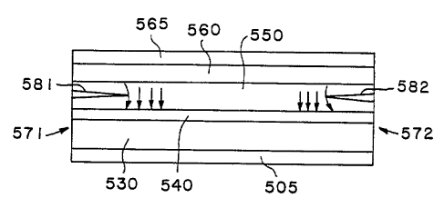
Figure 5 is a simplified cross-sectional diagram of a
metallized and oxidized device fabricated as described above.
The cross-section is taken longitudinally along the laser
stripe. In the Figure 5 diagram the bottom electrode is
labelled 505, the n-type lower confining layers are labelled
530, and the layers of the active region (at the p-n junction,
where carrier recombination occurs and light is produced) are
CA 02187354 2005-09-14
12
represented at 540. The p-type upper confining layers are
labelled 550, and the conductive cap layer is labelled 560 and
the upper metallization is labelled 565. The left edge cleave.
is labelled 571 and the right edge cleave is labelled 572. In
the illustration of Figure 5, the oxidation spikes (windows)
are formed, as described above, by lateral oxidation mostly in
the 1000 Angstrom high-aluminum-content layer of the upper
confining region, and are represented at 581 and 582,
respectively. The small vertical arrows represent current and
illustrate how windows are generally understood to reduce
current flow near the cleaved facets.
The foregoing example illustrates the advantages of the
invention in a III-V semiconductor laser, but it will be
understood that advantages can also accrue in other III-V
semiconductor devices, examples being non-lasing light
emitters (such as light emitting diodes), light detectors
(such as photodiodes), and transistors (such as field-effect
transistors).
Fig. 6 illustrates, in simplified form, an example of a
light emitting diode of a type that can be fabricated using
the technique of the invention. In this example, the
structure can be similar in geometry and materials to that of
the laser diode described in conjunction with Figures 1-5,
except that there are no cleaved facets. The light emitting
diode includes the following structure: bottom electrode 605,
n-type lower confining layers 630, active region layers 640,
p-type upper confining layers 650, conductive cap layer 660,
and upper metallization 665.
In the case of this light emitting diode, fabrication can
be similar to that of the laser diode example, but cleaving to
get reflective facets is not necessary, so division of a
crystal into pieces can be implemented, for example, by sawing
and/or etching. Also, typically, the top electrode will not
include a stripe, and may, for example, have an aperture for
light to escape, although light can be emitted from any part
(e. g. top, bottom, or sides) of the device. In this example,
the diode has oxide spikes which are formed as previously
CA 02187354 2005-09-14
13
described and can, again, advantageously reduce current near
the device edges to improve reliability and life of the
device. The beneficial sealing effect at or near the end of
processing, and after metallization, provides the same type of
advantages previously described; i.e.; the oxidation of the
device serves to seal cracks and other structural defects in
any portion of the device formed of aluminum-bearing III-V
material that is exposed to the oxidation directly or via
cracks or oxidation growth.
Figure 7 illustrates, in simplified form, a field-effect
transistor which can be fabricated using a technique of the
invention wherein aluminum-bearing III-V semiconductor
material in regions) of the device are oxidized after
metallization to obtain a native oxide. In Figure 7 a channel
region 730 is deposited on a substrate 720, and source, drain,
and gate regions are defined under metallized electrodes 741,
742 and 743, respectively. Appropriate diffusions (not shown)
can be provided at the source and drain. In the illustrated
example, a layer of relatively high aluminum fraction (e. g.
Alo,9Gao,lAs) aluminum gallium arsenide can be deposited and
defined over the gate region prior to metallization. Then,
after metallization (and, if desired, division of a crystal
with multiple devices formed thereon), wet oxidation can be
implemented, in the manner previously described, to form a
high quality insulating layer 750 between gate electrode and
channel. Again, the oxidation of the device serves to seal
cracks and other structural defects in any portion of the
device formed of aluminum-bearing III-V material that is
exposed to the oxidation directly or via cracks or oxidation
growth.
The invention has been described with reference to
particular preferred embodiments, but variations within the
spirit and scope of the invention will occur to those skilled
in the art. For example, it will be understood that the
techniques hereof can be applicable to fabricating other
device configurations and that other materials can be
employed, consistent with the claims set forth.