Note: Descriptions are shown in the official language in which they were submitted.
wo gsn797l 2 1 ~ 7 5 2 1
1
FF~nFl F :TFTC LIQUID C~YSTAL DISPLAYS WITil GREYSCALE
This lnvention relates to the multiplex eddressing of bistable liquid crystal
displays with greyscale, particularly ferroelectric liquid crystal displays.
Liquid crystal display devices are well known. They typically co~prise a
liquid crystal cell formed by a thin layer of a liquid crystal material held
between two glass walls. These walls carry LLc~ Lellt electrodes which apply
an electric field across the liquid crystal layer to cause a reorientation of
the molecules of liquid crystal material. The liquid crystal molecules in
~any displays ~dopt one of two states of molecular ~ .IL. Information
is displayed by areas of liquid crystal material in one state contrasting with
areas in the other state. ~)ne known display is formed as a matrix of pixels
or display elements produced at the intersections between column electrodes on
one wall and line (or row) electrodes on the other wall. The display is often
addressed in a multiplex manner by applying voltages to successive line and
column electrodes.
Liquid crystal materials are of three basic types, nematic, cholesteric, and
nmectic each having a distinctive molecular ~- ~ t.
The present invention concerns ferroelectric smectic liquid crystal materials.
Devices using this material form the surface stabilised ferroelectric liquid
crystal (SSFLC) device. These devices can show bistability, ie the liquid
crystal molecules, more correctly the molecular director, adopt one of two
aligned states on switching by positive and negative voltage pulses and remain
in the switched state after removal of the voltage. The two states can appear
as dark (black) and light (white) areas on a display. This bistable behaviour
depends upon the surface alignment properties and chirality of the material.
A characteristic of SSFLCs is that they switch on receipt of a pulse ofsuitable voltage amplitude and length of time of Arrl;rAtirn, ie pulse width,
termed a voltage time product V. t. Thus both amplitude and pulse width need
to be considered in designing multiplex addr~ing schemes.
WO 95~27971 2 1 8 7 ~ 2 ~ 14
There are a nu=ber of know~n systems for multiplex addressing ferroelectric
displays; see for example article by ~arada et al 1985 S.I.D. Paper 8.4 pp
131-134, and Lagerwall et al 1985 I.D.R.C. pp 213-221. See also GB
2 ,173, 336-A . and GB 2 .173, 629-A . Multiplex adùressing schemes for SSFLCs
employ a strobe waveform that is applied in sequence to lines but not
necessarily to successive lines simultaneously with data waveforms applied to
eg column electrodes.
There are two basic types of addressing. One uses two fields of addressing
with a first strobe (eg positive strobe) in a first field, followed by a
second strobe (eg negative strobe) in a second field; the two fields making
up a frame which is the time taken to completely address a display. The
other type of addressing uses a blanking pulse to switch all pixels in
one or more lines to say a black state. followed by a single strobe pulse
applied seq~ n~iA~ly to each line for selectively switching pixels in that
line to a white state. In this blanking addressing system the frame time is
the time required to blank plus the time taken to strobe all the lines.
The bistability property. together with the fast switching speed, cakes SSFLC
devices suitable for large displAys with a large number of pixels or display
elements. Such ferroelectric displays are described for example in:- N A
Clark and S T Lagerwall, Applied Physics Letters \/ol 36, No 11 pp 889-901,
June, 1980; GB- 2 ,166, 25 6-A, us-4, 367 . 924; us-4, 5 63, 059; patent
GB-2,209,610; R B Meyer et al, J Phys Lett 36, L69, 1975.
For many displays two visible states only are required, ie an ON state and an
OFF state. Examples of such displays include alpha numeric displays and line
diagrams. There is now an increasing requirement for a plurality of visible
states between the ON and OFF states, ie a plurality of different contrast
- levels. Such different levels are termed greyscales. Ideally the number of
greyscales should be around 256 for good quality pictures, but worthwhile
displays can be achieved with much lower values, eg 16 or less. :~
WO95127~71 21 ~7521 r~ J
There are two known techniques for providing greyscale; temporal, and spacial
dither. Temporal dither involves switching a pixel to black for a fraction of
a frame time and white for the remainder. Providing the switching speed is
above a flicker threshold (eg above about 35Hz), a user's eye integrates over
a period of time and sees an intPrmr~ t~ grey whose value depends upon the
ratio of black to white time. Spstial dither involves dividing each pixel
into individually switchable subpixels which may be of different size; each
3ubpixel i8 sufficiently small at normal viewing distances that subpixels can
not be distinguished individually. Both temporal and spacial dither
tr-rhniq~ c can be combined to increase the number of greyscale levels in a
display; see EP9000942, 0453033, W Hartmann, J van ~aaren.
Patent specification EP-0,214,857 describes a ferroelectric liquid crystal
display with greyscale. Greyscale display is achieved by addressing each line
of display with three successive equal period frame times, applying a scanning
voltage at the beginning of each frame and blanking once per frame at a
different time position within the three frames (other specifications would
describe these three frames as three fields making up a single frame time).
This gives a display with three different time periods when the display can be
in a light state; these together with an all dark state gives eight different
levels of greyscale. One disadvantage with this ~ ..t is a low maximum
light intensity from the display.
Patent specification EP-261,901 describes a ferro electric liquid crystal
display with greyscale. The time to address a complete display, namely a
frame time, is divided into fields of different lengths, hence a pixel can be
switched into a light or a dark state for a time approximately equal to the
length of each field. Each line is completely addressed in one frame time. A
line is addressed (switched to an ON or OFF state) at the start (for a
particular line) of each field time. To obtain a binary increase in greyscale
levels the length of each field would increase in binary manner. For any
reasonable number of lines to be addressed it is not possible to increase the
length of each field in the desired progression in order to achieve a desired
separation be~ween the different levels of greyscale.
21 87521
3a
Patent Specification GB-A-2164776 is similarto EP-261,901 in having different
length field times within a frame time. Pixels can be either light or dark in each field
5 time. Thus a total of six different levels of greyscale are obtainable from 3 different
length field times.
Patent Spe~ifi~itinn EP-A--0306011 describes a driving method for matrix of column
alld row electrodes in a r~.lu~,L,~Llic liquid crystal display. A frame time is divided
o into three unequal length field times. The driving method comprises: dividing, the
column electrodes into K groups of column electrodes, defining the number Z of
column electrode lines ,,oll~LiluLillg each group ofthe column electrodes, rendering one
frame period, selecting a ~ " " " ~l one of the K groups of the column electrodes
for a time width ZTo of each of the blocks so that each picture element on the selected
5 one of the ~roups of the column electrodes can be set in one of the bright and darlc
memor~ states, and selecting a number of times not smaller than n the K groups of the
column electrodes during each one-frame period TF according to a ,u.
sequence
AMENDEO SIIEET
WO 95127971 2 1 8 7 5 21 r~ b ~
4
One problem with existing addressing systems is that of providing
different greyscale levels that are suitably different in intensity, and
with a high overall display brightness.
Even with a combination of temporal and spacial dither it is still difficult
to provide a suitable spacing of greyscale levels.
The present invention overcomes the present limit of greyscale levels by
varying the relative positions of blanking and addressing pulses used to
address each line of a matrix display.
According to this invention a method of multiplex addressing a bistable liquid
crystal display formed by the intersections of an m set of electrodes and an n
set of electrodes across a layer of smectic liquid crystal material to provide
an mxn matrix of addressable pixels comprises the steps of:-
generating m and n waveforms for applying to the m, n electrodes. such-waveforms comprising voltage pulses of various dc amplitude and sign;
applying an m-waveform to each electrode in the m set of electrodes in a
sequence whilst applying appropriate one of two n-waveforms to the n set of
electrodes to address each pixel along a given m electrode into a required
state;
Characterised by the steps of:-
addressing each pixel a first time and a second or more times in a given frametime. the addressing being by application of a blanking waveform
followed or preceded by a strobe waveform in I ' n~t~nn with one of two data
waveforms, the time between application of blanking and strobe being an
addressing time; and
varying the addresslng time and relative times of addressing each pixel within
the frame time to provide a uniform greyscale intensity interval between
different greyscale levels.
21 ~7521
.
The addressing may be by a frst blan~6ing and strobe, and a second or more blanking
and strobe pulse in ~ " "1,; " ~ ;.... with two data wavefomms.
5 Altematively, two sets of strobe pulses may be used in ~mhin~lti~n with two data
wavefomms.
The pixels in a display may be complete pixels or pixels fommed by rf~rnhin~ti~n~ of
two or more subpixels of the same or different sizes.
~he rÆlative imtensifies of adjacent subpixels may be the same or different.
o According to this mvention a multiplex addressed liquid crystal display comprises:-
a liquid crystal cell includmg a layer of f~ u~ smectic liquid crystal material
contained between two walls, an m set of electrodes on one wall and an n set of
electrodes on the other wall arranged to fomm collectively an m,n matrix of a~ l,le
pixels:
wavefomm generators for generating m and n wavefomms comprising voltage pulses of
various dc amplitude and sign in successive time slots (ts) and applying the wavefomms
to the m and n sets of eleqtrodes through driver circuits;
20 means for controlling the application of m and n wavefomms so that a desired display
pattem is obtained,
i by:-
~5 means for addressing each pixel a first time and a second or more times in a i~enframe time, the addressing being by application of a blanliing ~avefomm follov~ed or
AMEN~ED SHEET
21 87~21
Sa
preceded b~ a strobe waveform in .;. ,.. ~,;..~1;.... with one of two data waveforms, tne
time between applicatiorl of blanking and strobe being an addressing time; and
varying the addressirlg time and relative times of addressing each pixel within the
frame time to provide a required greyscale intensity interval
~et~ differerl~ g~yscsle levols~
AMENDED SHEET
W095127971 ;i`~ 87~1 r~ ss~ ~14
Temporal weighting can be changed by changing the number of time periods in a
frame time and the position of the two addressing pulses in that frame time.
However, there are practical difficulties in providlng the desired ratios
between the two or more possible different switched states (Tl:T2) the
temporal ratio. The temporal ratio can be changed from that provided by the
relative positioning of addressing pulses within a frame time, by varying the
positions of blanking pulses relative to the strobing pulses.
Additionally, each pixel may be divided into subpixels of different or
similar area, and each subpixel addressed with different levels of greyscale.
~o provide a subpixel of s~all ~limPncinnc, the relative greyscale levels
between adjacent subpixels may be varied to change the apparent relative size
of the adjacent pixels.
W095/27971 2~ 21 P l/c~.r~l IJ
7
Brief description of drawings:
One form o~ the invention will now be described, by way of example
only, with reference to the , ying drawings in which:-
Figures 1, 2, are plan and section views of a liquid crystal displaydevice;
Figure 3 is a stylised sectional view of part of Figure 2 to a larger scale,
showing one of several possible director profiles;
Figure 4 is a graph showing switching Cl.aL~CI,=Listics of pulse width against
pulse voltage for one liquid crystal material;
Figure 5 is a di~hL tit'Al repr~c~ntAtinn of resultant voltages being
applied to a pixel in one line of a display;
Figure 6 is a diagram showing the address sequence for a four line display
with a temporal weighting of 1:3;
Figure 7 is an extension of Figure 6 showing how a 240 line display may be
addressed;
Figure 8 is a diagram showing one G~ lh___.lt for addressing a six linedi~pI47 with n teopor:l vei~hting Or 5:7~
WO 95/27971 2 1 ~ 7 5 2 1 P~ ..,,''C ~ 14
Figure 9 i8 a diagram showing one ~ t of addressing sequence for a
sixteen line displey having a temporal weighting of 1:3 modlfied by blanking
pulses to give e temporal weighting of 1:2 and a maximum brightness level of
21/32;
Figure 10 is a di2gram showing another /LLLCIIg_~ t of addressing sequence for
a sixteen line display having a temporal weighting of 1:2 and a maximum
brightness level of 30/32;
Figure 11 is a diagram shown a further ~lLLCllh~,__.lt of addressing sequence for
a sixteen line display having a temporal weighting of 1: 2 and a maximum
brightness level of 21/32;
Figure 12 shows waveforms for applying to lines and columns of a 16 line array
showing four lines ana four columns having four different grey scale levels;
Figure 13 is a modification of part of Figure 1 showing a different
t~L L ~le,~ .lt of line driver circuits;
Figure 14 is a view of one pixel divided into two subpixels in the ratio 1_2.
and;
Figure 15 is a view of one pixel divided into four subpixels in the ratio
1:2:2:4.
Figure 16 is a diagram showing an IlLL~le,~ , of addressing sequence for a 14
lines display with temperal ratio of 1:1.ô6:3.14.
W095/27971 2~1 87521 r~
Description of preferred embodiments.
The cell 1 shown in Figures 1, 2 comprises two glass walls. 2, 3, spaced about
1-6um apart by a spacer ring 4 and/or distributed spacers. Electrode
:iLLU~.l,UL~S 5, 6 of l.L~ISIJCL=II~ indium tin oxide are formed on the inner face
of both walls. These electrodes may be of conventional line (x) and column (y)
shape, seven segment, or an r-e display. A layer 7 of liquid crystal material
is contained between the walls 2, 3 and spacer ring 4. Polarisers 8, 9 are
arranged in front of and behind the cell 1. The alignment of the optical axis
of the polarisers 8, 9 are arranged to maximise contrast of the display; ie
approximately crossed polarisers with one optical axis along one switched
molecular direction. A d.c. voltage source 10 supplies power through control
logic 11 to driver circuits 12, 13 connected to the electrode ~,I,LU~I~ULI:~ 5, 6,
by wire leads 14, 15.
The device may operate in a transmissive or reflective mode. ln the former
light passing through the device e.g. from a tungsten bulb 16 is selectively
transmitted or blocked to form the desired display. In the reflective mode a
mirror 17 is placed behind the second polariser 9 to reflect ambient light
back through the cell 1 and two polarisers. By making the mirror 17 partly
reflecting the device may be operated both in a transmissive and reflective
mode with one or two polarisers.
Prior to assembly the walls 2, 3 are surface treated eg by spinning on a thin
layer of a polymer such as a polyamide or polyimide, drying and where
appropriate curing; then buffing with a soft cloth (e.g. rayon) in a single
direction Rl, RZ. This known treatment provides a surface alignment for
liquid crystal molecules. The molecules (as measured in the nematic phase)
align themselves along the rubbing direction Rl, R2, and at an angle of about
0- to 15 to the surface depending upon the polymer used and its subsequent
treatment; see article by S Kuniyasu et al, Japanese J of Applied Physics vol
27, ~o 5, May 1988, pp827-8Z9. Alternatively surface alignment may be
provided by the known process of obliquely evaporating eg. silicon monoxide
onto the cell walls.
WO95/27971 2 ~ 8 7 52 T~ l4
The surface alignment treatment provides an anchoring force to adjacentliquid crystal ma~erials molecules. Between the cell walls the
molecules are constrained by elastic forces characteristic of the
material used. The material forms itself into molecular layers 20 each
parallel to one another as shown in Figure 3 which is a specific
example of many possible structures. The Sc is a tilted phase in
which the director lies at an angle to the layer normal, hence each
molecular director 21 ca~ be envisaged as tending to lie along the
6urface of a cone, with the position on the cone varying across the
layer thickness, and each macro layer 20 often having a chevron
alJ,Jea' Gl~.r:.
Considering the material adjacent the layer centre, the molecular
director 21 lies approximately in the plane of the layer. ArrlirAtinn
of a dc voltage pulse of appropriate sign wilI move the director along
the cone surface to the opposite side of the cone. The two positions
Dl, D2 on this cone surface represent two stable states of the liquid
crystal director, ie the material will stay in either of these
positions Dl, D2 on removal of applied electric voltage.
In practical displays the director may move from these idealised
positions. It is common practice to apply an ac bias to the material
at all times when information is to be displayed. This ac bias has the
effect of moving the director and can improve display a~ a~ . The
effect of ac bias is described for example in Proc 4tb IDRC 1984 pp
217-220. Display addressing scheme using ac bias are described eg in
GB patent Arr~i'Ati"n number 90.17316.2, PCT/GB 91/01263, J 1~ Hughes
and E P Paynes. The ac bias may be data waveforms applied to the
column electrodes 15.
Figure 4 shows the switching characteristics for the material sCE8. Thecurves mark the boundary between switching and nonswitching; switching will
occur for a pulse voltage time product above the line. As shown the curve is
~btained for an applied ac bias of 7.5 volts, measured at a frequency of 50Hz.
W0 95127971 2 1 ~ 7 5 2 1 r~ 4
.
Suitable materials include catalogue references SCE 8, ZLI-5014-000,
av~ilable fro~ Merck Ltd, those listed in PCT/GB88/01004, W0 89/05025.
and: -
19.6% CM8 (49% CCl I 51% CC4) ~ 80.4% H
Me
CCl = C8HI7-~}OOC*H C6Hl3
Me Me
CC4 ~ CH2C*HC2Hs-<~}~COO{~CH2C*H C2H5
H1 = M1 ~ M2 ~ M3 ( 1 : 1 : 1 )
Ml = C8Hl7~}COO~}C5H
M2 = C8HI,O {~COO~C5HIl
M3 C781sO {~C00-~}C7Hls
.
WO 95127971 2 1 8 7 5 2 ~ 5 ~ - 14
1~ --
Another mixture is LPM 68 = Hl (49.5%), AS 100 (49.5%), IGS 97(1%)
Hl = MB 8.5F ~ MB 80.5F + MB 70.7F (1: 1: 1)
AS100 = PYR 7,09 t Py9 9.09 (1: 2)
MP 8 . 5F = C8H~ } CO2 ~ CsH
MB 80 . 5F = C8Hl,O -~}~} CO2 -~}
F
M~3 70.7F = C,HlsO -(~ CO2 ~~ C7Hl5
PYR 7.09 = C~HI~{O ~ ~} CsHls
PYR 9.09 = CgHIg--~G~ OCgHlg
IGS 97 = C8Hl,0 ~ C02C*H - CH(CH3)2
CN
W095J2~71 2~ ~7521 r~ 3:'t~l4
.
13
In one conventional display a ( - ) blanking pulse is applied to each line in
turn; this causes all pixels in that line to switch to or remain black.
Sometime later a strobe waveform is applied to each line in turn until all
line are addressed. As each line receives a strobe, appropriate data-ON or
data-OFF waveforms are applied to each column simultaneously. This means that
each pixel in a line receives a resultant of strobe plus data-ON or strobe
plus data-OFF. One of these resultants is arranged to switch a pixel to
white. the other resultant leaves the pixel in the black state. Thus selected
pixels in a line are turned from black to white, whilst other pixels remain
black. The time taken to blank all lines then address all lines is a frame
time. The blanking and strobing are repeatedly applied in sequence. To
maintain net zero dc balance, the blanking pulses are dc bal~nced with the
strobe pulses. Alternatively, all waveforms are regularly inverted in
polarity .
This conventional type of display can only show two levels of greyscale. ie
black and white.
~r~ AnAti~n of temporal wei~hting.
Although a given pixel can only adopt two switched states. namely a dark (eg
black) and a light (eg white) ~ e~LculCe~ four levels of greyscale can be
provided by addressing each line twice per frame. To obtain the c~e~cllce of
a contrast level between black and white (eg a grey), the pixel is repeatedly
switched black for a time period T1 and switched white for a time period T2.
Providing such a switching is above a flicker frequency of about 35Elz, an
operator will observe a contrast level or greyscale between black and white,
eg grey. The darkness of the grey will depend upon the ratio of Tl:T2.
Providing T1 does not equal T2, then four different levels of intensity can be
observed, ie four levels of greyscale. When the pixel is black for T1 and T2
the pixel is black; when the pixel is white for T1 and T2 the pixel is white.
When Tl>T2 then dark grey is obtained when the pixel is black for T1 and white
for T2. and the pixel is light grey when the pixel is white for Tl and black
for T2. In practice it is difficult to provide the desired ratio between the
different levels of greyscale. Odd values of temporal ratios (T2:T4) are
quite easy to produce. even values are required but are difficult to obtain.
WO g5~27971 2 1 ~ 7 ~ 2 1 r~ JD ~l l4
14
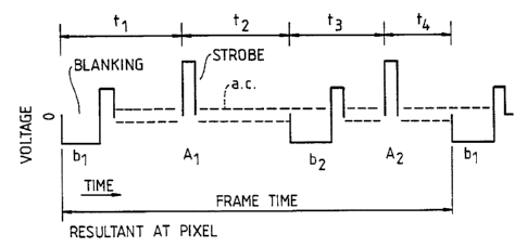
The principle of a uniform greyscale temporal addressing system i5 shown with
reference to Figure 5 which shows dic~;. t~rRlly a resultant waveform at
one pixel in a line being addressed.
As fihown in Figure 5 a plxel is swieched to black by a blanking pulse Vbl. A
time tl later the pixel is addressed by a strobe pulse Val. After a
furtber period of t2 a blanking pulse Vb2 again switches the pixel to black.
After a time of t3 a second strobe pulse Va2 sddresses the pixel. After
further time t4 the blanking pulse Vbl is applied and the process repeated.
The time between Arrlinnti~nC of the blanking pulse Vbl, ie tl t t2 ~ t3 ~ t4.
is the frame time of a display. Both strobe pulses Val and Va2 are
capable of switching a pixel to white or leaving it black.
This means that the pixel is always black for tl and t3. The pixel csn be
either black or white for period t2, and either black or white for period t4.
~y varying the period t2 and t4. the pixel can have the appearance of any two
greyscale levels between black and white as well as black and white. Varying
tl and t3 varies the overall display brightness.
The following table 1 shows different greyscales for addressing where t2>t4.
Table 1.
Period tl t2 t3 t4 Greyscale
State black white black white (almost) white
State black white black black light grey
State black black black white dark grey
State black black black black black
.
WO 9S/27971 2 1 8 7 5 2 1 r~ l4
15
Figure 6 shows a display having four lines; the number of columns is
~ 7. The number of line address time periods is eight. The letter A
is used to show addressing of a pixel in a given line; this is di~E,L
only and presumes blanking and immediate strobing in one time slot. L1 is
addressed in periods 1 and 3; L2 in periods 2 and 4; L3 in periods 5 and 7;
L4 in periods 6 and 8. Thus a pixel can be say black for 2 time periods and
white for 6 periods, ie~a greysca_e temporal weighting of 1:3. The greyscales
are 0/8; 2/8; 6/8; 8/8, ie interva_s of 1:3, and 3:4.
WO 95127971 2 1~ 2 1 r~ 14
16
This can be extended to much larger displays by addressing the lines ingroups, and dividing the time periods into sub periods. For example in
Figure 7 the lines are grouped as lines 1~4q, lines 2+4q, lines 3~4q, lines
4+4q where q is an integer, eg 1 to 60 giving a total o~ 240 lines. Each
period is then divided into 60 subperiods. Line 1 is addressed in subperiod 1
of period 1; line 5 (1~4q q=1) is addressed in subperiod 2 of period 1; line
9 ~1~4q, q=2~ is addressed in subperiod 3 of period 1, etc until line 237 is
addressed in subperiod 60 of period 1. Then line 2 is addressed in subperi~d
1 of period 2, lines 6 .... 238, lines 3....239, lines 4...240 etc. However,
the greyscale temporal ratio is still 1-3 which does not give a linear spacing
of the greyscale levels.
Figure 8 shows the addressing of a six line display in a total of twelve time
periods. Line L1 is addressed in periods 1 and 6, other lines are addressed as
indicated. The position of the addressing pulse appears to move around
in a non ordered manner. The reason for this is the double requirement
of addressing each line twice in each frame time, and not being able to
address two different lines at the same time. The illustrated 12 periods
is only a snap-shot in time; the 12 periods repeat whilst the display is
in operation. Each pixel can be in say a black state for 5 time periods and
a white state for 7 time periods. The greyscale weighting is 5:7 which is
still not a linear spacin~ of greyscale levels.
Figure 9 shows the addressing of 16 lines over 32 periods, the figure shows a
snapshot over 32 periods. This would normally give a temporal weighting of
1:3 with both blanking pulses preceding the strobing pulse by the same
minimum interval. Blanking pulses are arranged so that the temporal weighting
is 1:2. As shown the strobing pulses are in the time ratio 8:24, ie 1:3.
Taking the times indicated in Figure 5, then Figure 9 gives tl=10; t2=7;
t3=1; t4=14. This gives the following greyscales--
.. -
W0 95J27972 ~ ~ ~ 7 ~ 2 ~ r~ s ~ 14
17
Table 2
Level of white
bbbb - black for all 32 periods 0
bwbb - black for 25 ar,d white for 7 periods 7
bbbw - black for 18 and white for 14 periods 14
bwbw - black for 11 and white for 21 periods 21
This .., ~ t gives a maximum brightness of 21/32.
Clearly this can be extended for a 256 line display by arranging the 16 lines
in groups of 16 and dividing each period up into 16 subperiods as explained
earlier .
Figure 10 shows the addressing of 16 lines in 32 time periods with strobing
pulse S i ' Atl~ly preceded by blanking pulse b. The two periods where the
display can be white are 20 time periods, and 10 time periods. The temporal
weighting is thus 10:20 ie 1:2 which is an even weighting. The maximum
brightness is 30/32. ~owever, the effect of blanking just before strobing
is to slow down switching of the liquid crystal material.
It is common to blank a few lines ahead of strobing; typically blanking is
4 to 7 lines ahead of strobing and reduces switching times. Taking the
". . ~.,,___.IL of Figure 10 and making the blanking occur 4 lines ahead of
strobing results in a temporal weighting of 7:17 which is not an even
weighting. The maximum brightness is 24/32.
Figure 11 shows the addressing of 16 iines in 32 time periods. In every line
one blanking pulse is 4 lines ahead of strobing, and the other blanking
pulse is ahead of strobing by 7 lines. The display can be white for both 14
and 7 time periods, ie a temporal welghting of 7 :14 . which is an even
weighting. Maximum brightness is 21/32.
WO 95/27971 2 1 8 7 5 2 1 P~ 14
18
Waveforms for addressing a 16 line 4 columns matrix with four levels ofgreyscale are shown in Figure 12. Shown are 4 of the 16 lines and columns
marked 1. 2, 3, 4, with each line and column intersection left unshaded,
lightly shaded, darkly shaded, or completely black, to respectiveIy indica~e
white, light grey, dark grey, and black. Line 3 is marked to show white,
light grey, dark grey, and black in columns 1, 2, 3, 4 respectively.
Waveforms applied to the lines (rows) are shown; they comprise blanking
pulses -Vb, and strobe pulses ~Vs, applied twice per frame time. Column
waveforms are ~/- Vd pulses each pulse lasting one time slot ~ts). The
illustrated pattern of colu_n waveforms provide the greyscale pattern of
display shown. The resultant waveforms at pixels A, ~, C, D in line 3 are
shown. Under each resultant is a graPh showing light trPr1cn~ic~;rn through the
AC~:r/r1Atl~d pixel pixel A shows the most time with a high trAncmi~cinn and is
therefore the lightest, ie white, pixel. In contrast pixel D has zero
trAn -m; CC~ r~n and is therefore black .
The addressing of a 16 line matrix can be expanded to 256~1ines or more as
described above by addrassing lines; 1, 17, 33, 49 - 241; 7, 23, 39, 55, -
246; 2, 18, 34, 5O - 242. Increasing the number of colu. ns does not affect
the complexity.
One circuit for addressing a 16 or _ore line displAy is shown in Figure 13;
it modifies the line driver circuits of Pigure 1; no change is needed for the
column driver. As shown in Figure 13 four line drivers are used 20, 21, 22,
23. Line driver 20 has its successive outputs connected to lines 1, 5, 9, 13
etc; line driver 21 has its successive outputs connected to lines 2, 6, 10,
14; line driver 22 has its successive outputs connected to lines 3, 7, 11,
15, and line driver 23 has its successive outputs connected to lines 4, 8, 12,
16. This LIL ' r~~ t can be cascaded to use all driver outputs, eg the
addressing of 256 lines by using 64 driver outputs.
WO 95127971 2 1 ~ 7 5 2 1 r~
19
In a =odification, blanking pulses are replaced by strobes. This requires
four subframes of addressing in order to obtain four different periods of
switched states.
Explanation of spatial weighting.
.
A pixel can be divided up into a number of areas of equal or different sizes.
The epparent darkness of a pixel is related to the area of black compared to
the area of white. For example Figure 14 shows a pixel divided into 2 areas
in the ratio of 1:2 which could be arranged to be consecutive lines of a
display. This ~llows 4 greyscale levels, ie both areas black, both
areas white, the large area black with the other white, and the large
area white and the other black. Figure 15 shows a pixel subdivided into 4
areas in the ratio 1:2:2:4 which allows a total of 10 levels. This requires
two adjacent lines and columns per pixel.
In high resolution displays the overall size of a pixel can be quite small eg
25x25um, subdividing the pixel can cause difficulties ln manufacturing the
s~allest subpixel. This problem may be overcome by varying the apparent size
of a subpixel. The apparent size of one subpixel relative to an adjacent
subpixel is related both to the area of the subpixels, and to their relative
brightness. Thus by making the smallest subpixel darker than its neighbour,
then the smallest subpixel appears to be even smaller than its physical size
would indicate. This allows the subpixel to made slightly larger in area than
ex~ected Eo~ en greys~ e ~eve1.
W095127971 ~3i~7~S~ '`'1'''~'s'~ 14
The greyscale level (and hence relative darkness) of one subpixel relaeive to
another may be altered by varying the time between blanking and addressing
pulses shown in Figure 5, ie Yarying tl+t3 in adjacent lines. This varies
the length of time spent in a black state in the different greyscale levels.
As described above, uniform greyscale levels in a display may be achieved by
temporal weighting alone, or in ~ ' n~tinn with spatial weighting.
Furthermore the spatial weighting may be modified to varying the apparent size
of adjacent subpixels.
For example 256 greyscales say be provided by the following nAt;nnc -
Table 3
Temporal Ratio Spatial Ratio
1:2 1:4:16:64
1:4 1:2:16:32
1:16 1:2:4.8 _ _
It may not be desirable to produce linearly spaced grey levels. The eye does
not respond linearly to uniform increments of brightness, the apparent
difference in lightness between adjacent levels being much less at the light
end of the scale than at the dark end ~R ~ G ~3unt, Measuring Colour. second
edition, published by Ellis Horwood Ltd, 1991).
A feature of the present invention, is that any desired weighting may be
obtained by addressing the lines in the required ~IIUII ' ~ .t; sll ) sequence and
making correction to any small errors in the weighting by use of the variable
blanking to strobe separation. The required addressing sequence, for a
required temporal ratio of rl:r2:r3:..:r~ (x is number of bits of greyscale),
may be arrived at from the following algorithm which will be correct as kl (the
number of lines) t~ L~C~ a infinity:-
wo g5n7971 2 1 ~ 7 5 2 1 r~/(.L~ c 14
21
(I; r2 +r3 + -- + 3x+1; r3 + .. + ry+1; ...... ; rx+l) first bracket
(2; r2 +r3 + -- + 3x+2; r3 + .. + rX+2; ...... ; ry+2) second bracket
(3; r2 +r3 + -- + 3x+3; r3 + .. + rx+3; ...... ; rx+3) third bracket
(R; r2 +r3 + -- + 3x+R; r3 + .. + rx+R; ...... ; rx+R) Rth bracket
Where R equal the summation of ri (for i=1 to x) and where the addressing
sequence follows the first bracket for the first R lines, then th2t sequence
is repeated on the next R lines until all (M/R) groups of lines have been
addressed, then the addressing sequence follows the second bracket for all
(M/R) groups of lines, and so on until the sequence has followed the Rth
bracket to all (M/R) groups of line; modulo R arithmetic is used to keep
the nu=erical expression within the relevant group of R lines.
The actual temporal ratios will be given by:-
(rlxN)+R: (r2xN)+R: ... :rx lxM: rxxN-(x-l)R
For example consider a desired temporal ratio of 1:2:4 ~nd a total of 14
lines. Then rl-1, r2=2, and r3=4, (rX=r3=4), x=3 the number of temporal bits,R=1+2+4=7, and M=14.
The addressing sequence of lines is :-
first group of R lines second group of R lines
first bracket 1, r2+r3 1, r3 1 7+1, 7+r2+r3+1, 7+r3+1
W09~/27971 2~ 2 1 P~ . 14
Z2:
Substituting values this becomes:-
first bracket 1, 2+4+1~ 4+1 7+1, 7+2+4+1, 7+4+1
second bracket 2, 2+4+2, 4+2 7+2, 7+2+4+2, 7+4+2
third bracket 3. 2+4+3, 4+3 7+3, 7+2+4+3, 7+4+3
fourth bracket 4, 2+4+4, 4+4 7+4 . 7+2+4+4, 7+4+4
fifth bracket 5. 2+4+5, 4+5 7+5, 7+2+4+5, 7+4+5
sixth bracket 6. 2+4+6, 4+6 7+6, 7+2+4+6, 7+4+6
seventh bracket 7. 2+4+7, 4+7 7+7, 7+2+4+7, 7+4+7
This gives the following sequence of addressing, showing the modulo conversionthus (x>)x-7:-
first group o~ R lines second group of R lines
first bracket 1, 7. 5. 8, 14, 12
second bracket 2, ~13>)1, 6 9. (15>)8, 13
third bracket 3. (9>)2, 7 10, (16>)9, 14
fourth bracket 4, (10>)3, ~8>)1 11, (17>)10, (15>)8
fifth bracket 5, (11>)4, (9>)2 12, (18>)11, (16>)g
sixth bracket 6. (12>)5, (10>)3 13, (19>)12, (17>)10
seventh bracket 7, (13>~6, ~11>)4 14, (20>)13, (18>)11
The temporal ratio is 7:13:2Z which is 1:1.86:3.14. Thisaddressing sequence is illustrated in Figure 16, where the solid squares
represent addressing, ie blanking followed by strobe.
The actual temporal ratio will be given by:-
(1 x 3 x 14)+7: (2 x 3 x 14)+7: (4 x 3 x 14)-(3-1)7
ie 49: 91: 154 which is 1: 1.86: 3.14 ~