Note: Descriptions are shown in the official language in which they were submitted.
2 1 87582
EDGE TERMINALS FOR ELECTRONIC CIRCUIT MODULES
Field of the Invention
The present invention pertains to the field of electronic modules,
including single or multi-chip modules and hybrid circuits, and methods for
fabrication of such modules. Specifically, the invention pertains to improved
edge connectors for such modules, which are formed of heat resistant metal,
flush along the edge of the module, which permit a reduction in physical size ofthe module, and simpler and more reliable connections to the module during
assembly or reassembly of the module on a circuit board or other support where
the module will be used.
B~-~k~round of the Prior Art
One general type of circuit module in widespread use today
involves one or more integrated circuit (IC) chips and possibly additional
discrete components mounted on a substrate which has metalization and
multilayer interconnects, with the assembly potted in epoxy. Such circuits are
often referred to as electronic modules, multi-chip modules (or single-chip
modules) or hybrid circuits. For convenience of terminology herein, such
circuits will be referred to as electronic modules, and it will be understood that
this term includes single or multiple chip modules, with or without additional
discrete components.
Typically, the fabrication of such electronic modules starts with a
relatively large substrate on which multiple individual modules will be built up,
with the substrate to be subsequently cut into a number of relatively smaller
pieces which become the individual electronic modules. The substrate is built upwith metalization layers and multilayer interconnects, as is generally known in
the art, in order to provide the appropriate interconnects and signal traces
according to the function and design purpose for the module. One or more ICs
are then mounted on the surface of the substrate and connected to the signal
traces. Additionally, in hybrid circuits, discrete components such as capacitorsmay also be mounted. In one type of commonly used interconnect, the IC has
21 87582
solder bumps on its terminal pads which overlay and contact corresponding
signal trace pads on the substrate. The assembly is heated to cause the solder to
melt or flow to make a permanent electrical connection. In another commonly
used type of interconnect, the ICs are mounted on the substrate, and flying lead5 wires are applied from terminal pads on the chip to corresponding signal trace pad on the substrate.
The entire side of the substrate on which the chips or the
components are mounted is then potted in epoxy, and after the epoxy cures the
substrate is cut along predetermined lines to separate the individual modules.
One commonly used technique for applying the epoxy potting
material to the module was developed by the assignee of the present invention,
and involves forming small ceramic pieces and gluing them all the way around
the edge of the substrate to form an dam for the epoxy. The ceramic pieces are
formed with a length according to the side dimensions of the substrate, and of al S height selected in accordance with the depth or thickness of the intended epoxy
layer, so as to contain the epoxy as it is poured onto the surface to cover the ICs
and other components. After the epoxy has cured, the cutting process cuts
through the entire composite skucture, substrate and epoxy, along predetermined
paths (generally a grid) to separate the individual circuit modules.
In use, the circuit modules may be bonded or otherwise mounted
to a circuit board or other support structure, according to the intended use of the
specific application design. Electrical and electronic connections for the module
are made to pads formed on the non-epoxied side of the substrate, which connect
through internal vias to the appropriate multilayer signal traces and/or the chips,
according to the circuit design of the module. Circuit modules produced by this
fabrication technique have very good electrical and mechanical properties, and
have proven to be very successful and reliable in a great number of applications.
Although the prior art electronic module construction described
above has been very successful, it has been appreciated that certain
improvements would be desirable in the terminals or interconnects from the
module to the circuit board or other application environment in which the circuit
module will be used. It would be desirable to have the interconnects on the
- 21 87582
electronic module larger and more robust, so they are less fragile and easier toconnect to. However, making them larger would use up more surface real estate
area on the module, and this is usually limited by the fact that there may be a
large number of terminals needed in a particular design. As a result, connections
5 to these terminals must be done very carefully in order to avoid ~ ging,
dissolving or overheating the terminal during assembly. Because of these
problems, it is usually not possible to rework, reuse or repair such modules, due
to the potential for damage to the terminals caused by heating them.
More recently, it has been proposed to provide a terminal along
10 the edge of the electronic module, in the form of recesses or wells filled with
solder. According to such proposal, holes are provided through the substrate,
positioned in the area which will later be cut when the substrate is cut up into the
individual circuit modules. These holes are metalized, and connect to
appropriate traces on or in the substrate. The holes are then filled with solder,
15 which adheres to the metalization. The solder-filled holes are then buried along
with the chips and other components during the epoxy potting process. As the
substrate is cut into the individual modules, the solder-filled holes are bisected,
and the cut surfaces then form edge terminals for the individual modules. These
terminals are flush with the edge, are formed of solder, and extend partway
20 through the thickness of the module, specifically through the substrate portion,
but not the overlaying epoxy portion. Edge terminals provide the advantage of
not requiring surface area on the electronic module for interconnection, which
allows for a smaller electronic module. However, such terminals still are small
and difficult to connect to, and they can dissolve away if they are overheated, or
25 if there are multiple heatings, for example, during an attempted rework or repair.
To overcome these and other problems, the present invention has
provided an improved type of edge terminal construction for small electronic
modules, which provide flush edge connections to thereby reduce the need for
surface area and permit a smaller module, but which are robust, relatively simple
30 to connect to, and which can withstand overheating, and multiple heating for
rework or repa1r.
21 87582
Summar,v of the Invention
These and other objects are accomplished by providing an
improved edge terminal for a circuit module, consisting of bars of substantiallyheat resisting metal embedded along the edge and flush with the edge of the
S circuit module. The heat resisting metal is a metal which is not solder or any
other material that melts at normal soldering temperatures. In one embodiment,
the terminal extends substantially through the full thickness of the circuit
module. This embodiment is preferably made by forming holes in the substrate
along the paths where the cutting will take place to separate the individual
modules, placing pins or bars, preferably of copper or some other heat resistantmetal, in the holes in contact with traces therein or thereon, and epoxying themin place in the otherwise standard potting process. When the cut is made, it is
made through the center of such a pin or bar, essentially bisecting it, so that half
goes with and forms an edge connector for one module, and the other half forms
an edge connector for the adjacent module.
According to another embodiment of the invention, the heat
resistant metallic terminal extends along the edge, flush therewith, for
substantially the thickness of the potting material. This embodiment is formed
by placing bars or pins on the substrate prior to potting. These bars are soldered
or other~,vise attached to conductive trace paths on the surface of the substrate, or
in recesses formed therein, and essentially straddle the zones or lines where
cutting will eventually take place. After potting, the individual circuit modules
are separated by cutting through the bars or pins, leaving part of a bisected bar as
a terminal for one circuit module, and the other part for another one.
These and other advantages of the present invention will become
apparent from the following detailed description of the preferred embodiments ofthe invention.
Brief Description of the Draw;ng
In the drawing, Figure 1 is a view in perspective, at an enlarged
scale, of a circuit module having edge termin~ls7 according to one embodiment
of the invention;
21 87582
Figures 2-7 illustrate various steps in the formation of circuit
modules of Figure 1 from a large substrate which is subsequently cut into the
individual modules; Specifically,
Figure 2A is a plan view of a large substrate showing an array of
individual cells, which will correspond to the individual circuit modules, each
cell having circuit components and being bordered by rows and columns of
mounting holes;
Figure 2B is a view at enlarged scale of a detail of Figure 2A;
Figure 3A is a view similar to Figure 2A, but without components
installed, showing the mounting hole patterns;
Figure 3B is a view at an enlarged scale of a detail of Figure 3A;
Figures 4A and 4B show sections of terminal bars, horizontal and
vertical, respectively, used in the embodiment of Figures 1-7 to form edge
terminals;
Figure 5 is a view showing terminal bars assembled on the
substrate for the encapsulation step;
Figure 6 shows a substrate after encapsulation;
Figure 7 shows the sawcut paths over the substrate to separate the
individual circuit modules;
Figure 8 is a view similar to Figure 1 of a circuit module, having
a different type of edge terminal according to an alternate embodiment of the
invention;
Figure 9A is a view of a lead frame used in forming edge
terminals according to this alternate embodiment;
Figure 9B is a view at an enlarged scale of a detail of Fig. 9A;
Figure 9C is a view similar to Figure 9B of a detail of a variation
of the alternate embodiment;
Figure 10 is a view of the encapsulation step of this alternate
embodiment; and
Figure 11 is a diagram showing the sawcut paths of the finished
substrate to form the individual circuit modules.
21 87582
Detailed Description of the Preferred Embodiment
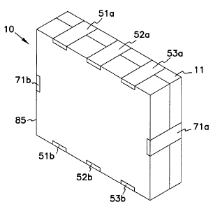
With reference now to Figure 1, an individual circuit module
according to the present invention is shown, at an enlarged scale. As seen in
Figure 1, module 10 includes a substrate 11, encapsulant 85, and is generally of a
5 rectangular shape, having been cut by sawing process from a larger substrate in
which an array of cut modules can be formed. The substrate may be formed of
ceramic, epoxy glass, or any other substrate material as may be used in electronic
fabrication. Substrate 11 includes multilayer signal traces as is generally known
in the art, and various components including one or more ICs and possibly
10 external resistors or capacitors are mounted on one or both sides of substrate 11,
but are not visible in the finished module in Figure 1, because they are potted or
covered by the encapsulant 85.
Module 10 also includes a number of edge terminal connectors
according to the present invention. Specifically, terminals 71 a and 71b are
15 provided on opposite ends thereof, and terminals 51a, 52a, 53a are provided on
one side, and 51b, 52b, and 53b on the opposite side. In each case, the terminalconsists of a metal structure embedded in both the encapsulant 85 and substrate
11, and flush with the outer edges of the module. These terminals provide
electrical connections between the circuit module and a circuit board or other
20 structure (not shown) with which the module was intended to be used.
Substrate 11 preferably has multilayer signal traces as is generally
known in the art, to form the necessary interconnections among the components
thereon, and the external edge terminals. Each edge terminal 71 a, 71b and 51 -
53, a-b, is connected to signal traces in or on substrate 11 according to the logic
25 design of the particular module.
Figures 2A and 2B show a larger substrate 111, which is built up
with an array or large number of individual circuits, which will subsequently becut into individual modules. As seen in Figures 2A and 2B, each circuit module
or cell includes an IC 20, and additional discrete resistor or capacitor components
30 22, 24, 26. These components connect through known techniques to signal tracepaths and holes provided in a substrate, as is generally known in the prior art, in
- 21 87582
accordance with the particular circuit function design for the modules. The
individual circuit cell is repeated a large number of times over the entire
substrate 111, so that the module cells form regular columns and rows, to aid insubsequent separation by cutting.
Also visible in Figures 2A and 2B are the rows and columns of
holes for use in forming the edge terminal. These are seen better in Figures 3A
and 3B, which are similar to Figures 2A and 2B, but without the components. A
plurality of horizontal (in the orientation of Figure 3A) rows are made up of a
series of holes 40a, 40b, 40c, and so on, which are provided along the boundary
l O between adjacent rows of module cells. Similarly, vertical columns of holes 60a,
60b, 60c and so on are provided in columns on the separation between adjacent
module cells. It will be understood that the use of the terms 'row' and 'column' is
somewhat albiLl~lr, as they can be used interchangeably depending upon the
orientation, and are adopted for convenience of terminology, and not in any
limiting sense.
In the preferred embodiment shown, the rows of holes 40 include
three individual holes along each side of the cell. These holes will eventually
correspond to the terminals 51, 52, 53 on either side of a finished circuit module.
Similarly, the columns of holes 60 provide a single hole on each end of a modulearea, and will correspond to the edge terminals 71 of the finished module (please
see Figure 1). It will be appreciated that the number of holes on the sides or end
can vary according to the size and circuit requirements of the individual moduledesign, and the preferred embodiment showing three on two sides and one each
on the other side is only by way of example, and not limitation.
The individual holes 40, 60 in the rows and columns are formed
in the substrate according to a predesigned pattern, and the holes intersect signal
traces on or within the multilayer structure on the substrate according to the
circuit design.
Figures 4A and 4B show, at an enlarged scale, bar structures that
are used to form the edge terminals. These bars are long enough to stretch across
the width of the array of circuit cells on substrate 111, and interlock to form a
21 87582
~,
grid aligned with the rows and columns of holes 40, 60, thereby forming a
perimeter around individual cells, as shown in Figure 5.
Figure 4A shows details of a horizontal bar 50, a plurality of
which are needed to cover substrate 111. Each bar 50 is an elongate barlike
structure made of a durable metal such as copper, nickel or zinc, to which solder
will adhere. As seen in Figure 4A, an upper edge of bar 50 has a plurality of
clearance/interlock notches 55, at regular intervals according to the pitch or
width of the circuit cell size. The other edge of bar 50 has a plurality of posts 51,
52, 53, separated by gaps 54, which are positioned generally opposite notches
55. The posts 51, 52, 53 are scored or partially etched with a break line at
location 56, where they join the main part of the bar. The break line is used tobreak the grid away after encapsulation, as described below. Horizontal bars 50
are configured for placing along the rows, with the posts 51, 52, 53 of each
group fitting in the group of corresponding holes 40a, 40b, 40c, etc. in the rows
of the substrate 111 (see Figure 3).
Vertical bars 70, as shown in Figure 4B, are generally similar to
horizontal bars 50, but are designed to fit with their posts 71 in the columns of
holes 60a, 60b, 60c, etc. Bars 70 have gaps 74 at intervals corresponding to thepitch or spacing of the circuit cells, with an individual post 71 positioned
therebetween to fit into the holes. A break line at location 76 is provided for
each post 71, in the same manner as the break lines 56 of the bars 50. Of course,
in different designs, there may be an additional number of posts in this location.
A clearance/interlock notch 75 is provided in each gap 74. Notch 75 in vertical
bar 70 cooperates and interlocks with notches 55 and horizontal bars 50, so that a
plurality of parallel spaced bars 50 can interlock with a number of parallel
spaced vertical bars 70 to form a grid of bars as shown in Figure 5.
After the bars are in place, solder is flowed around and/or into the
holes 40, 60, to surround and/or fill around all of the individual posts 51, 52, 53,
and 71, around each circuit cell over the entire substrate.
Epoxy dams are formed and attached around the edge of the
substrate as shown in Figure 5. Specifically, dams 80 and 82 are attached on
- 21 87582
opposite sides, and 81 and 83 are attached on the other opposite sides, to form a
contiguous dam or barrier having the desired height above substrate 111 for
flooding with epoxy encapsulant. This results in a structure as appears in Figure
6, after the encapsulant has been poured, covering all of the components of the
5 individual circuit cell, and extending partway up on the bar grid. The portions of
the bar grid extending above the encapsulant are removed at the breaklines 56,
76 which are shown on Figures 4A and 4B.
The substrate is then cut along the plurality of perpendicular
sawcut paths 45, 65, as shown in Figure 7, which bisect each of the horizontal
10 and vertical bars. This not only separates the overall substrate and assembly into
individual circuit modules, but also cuts through each of the terminal bars,
leaving only separate halves of the posts 51, 52, 53 as the embedded edge
terminal 51a, 52a, 53a, and 51b, 52b, 53b, of Figure 1. Similarly, the vertical
bars are cut through in this process, leaving separated halves of posts 71 on the
15 embedded edge terminal 71a, 71b of Figure 1. Since these edge terminals are
soldered to applopl;ate signal traces within or on substrate 11, and since they are
secured both by being soldered in substrate 11 and surrounded by encapsulant
85, they are very durable electrical edge connections for the individual module.In the embodiment shown in Figure 1, eight edge terminals are
20 provided. It will be appreciated that in the prior art structure wherein the
terminals would be provided by pads on a face of the substrate, there would be
limited surface area available for each terminal. Also, because such terminals
would be markedly small and in tracelike structures, they would be subject to
heat damage, mentioned above, in the case of soldering or reworking. In
25 contrast, the edge terminals of the embodiment of Figure 1 provide a more
substantial mass of metal to be attached to without damage, and therefore
provide for a more robust, compact circuit module.
An alternate embodiments is shown in Figures 8- 11. The module
seen in Figure 8 has a rectangular solid configuration, with substrate 12, an
30 encapsulant 85, as in the previous embodiment. The substrate 12 may be
generally similar to substrate 11 of the first embodiment, but the configuration
21 87582
will differ in the manner of attachment of terminals, as explained below. The
terminal 151a, 152a,, 153a, and 171a, are seen provided on module edges for
external connection. It will be understood that corresponding edge terminals
151b, 152b, 153b, 171b, are provided on the other two edges not visible in the
5 orientation of Figure 8 because they do not extend through the encapsulant. Inthis embodiment, the edge terminals are again flush with the sides and edges of
the module, and embedded in the encapsulant, but not in the substrate. The
terminals abut the surface of the substrate and are connected to appropriate
signal kaces thereon.
This embodiment is also formed on a large substrate having the
circuit design and component repeated in a number of rows and columns of
circuit cells which will later be cut and divided. This embodiment does not use
mounting holes for the terminals, but instead makes use of a lead frame 140 as
indicated in Figures 9A and 9B. The lead frame is formed of a durable
15 conductive material to which solder will easily adhere. It has a number of
horizontal rows 150a, 150b etc., and vertical columns 170a, 170b, etc. The
actual number of columns and rows depends on the particular design. The
spacing of the grid corresponds to the circuit cell dimension, such that the lead
frame grid columns and rows will be positioned exactly over the cut line to
20 separate the circuits. Each row portion 150 of lead frame 140 includes three
widened zones 151, 152, and 153. These will correspond to the edge terminals
151 -153, a,b, in the final module as shown in Figure 8. Similarly, each of the
column portions 170 of the lead frame have a widened zones 171, which will
correspond to the edge terminals 171 a, b in the finished module. The perimeters25 of the lead frame can have half-width zones 15 lp, 152p, 153p and 17 lp, as they
will form terminals on one module only, not two adjacent modules.
Lead frame 140 is placed over the substrate, with the columns and
rows of the lead frame exactly on the dividing lines which will be cut. They arethensolderedsothatthewidenedzones 151, 152, 153, 171 areelectrically
30 connected to tabs provided for that purpose for traces on the substrate.
21 87582
-
11
As an alternative to lead frame 140, small terminal plates or
structures 251, 252, 253, and 271 may be provided directly without a lead frame.
These terminal plates are also made of durable conductive material to which
solder will easily adhere. The arrangement of the terminal plates is shown in
5 Figure 9C, which is at the same scale and orientation as Figure 9B, so that the
correspondence can be seen between the widened zones on the grid and the
terminal plates. In the alternative embodiment of Figure 9C, the terminal plates
are placed on tabs provided for that purpose for traces on the substrate,
preferable by robotic assembly in the same manner as components. They are
10 soldered in place to make mechanical and electrical contact with the pads. They
will subsequently be cut after encapsulating, as described below. Half-width
terminal plates 251p, 252p, 253p, and 271p may be used for terminals around the
perimeter of the substrate 112.
The epoxy dams are then placed around the substrate as in the
15 first embodiment previously described, and epoxy or other encapsulant is poured
in, covering components on the substrate (not shown) and the lead frame 140,
indicated in Fig. 10, if one is used. The substrate is then cut along the sawpath
indicated in Figure 11, that is, down each of the rows 150 and columns 170 of
lead frame 140, which is at this point embedded within the encapsulant. The
20 width of the saw cut blade, in comparison with the width of the lead frame rows
and columns, is such that the saw cut blade consumes and elimin~tes the entire
lead frame, except for the edges ofthe widened zones 151, 152, 153, and 171,
each of which is bisected to form edge terminals on adjacent circuit modules as
they are being cut. If no lead frame is used, the saw cut blade separates the
25 terminal plates 251, 252, 253, and 271, each of which is bisected to form edge
terminals on adjacent circuit modules as they are being cut.
The resulting circuit module, as shown in Figure 8, again has the
advantage of edge terminal placement, rather than requiring surface placement of
connections, thereby allowing for greater mini~t~lrization. Also, the edge
30 termin~l~, while not as long or massive as those in the embodiment of Figure 1,
are still made of a substantial piece of metal, rather than a trace, and are therefore
21 87582
-
12
more robust and durable in manufacturing or reworking processes than prior art
deslgns.
It will be appreciated from the foregoing that the present
invention provides an improved edge terminal construction for small circuit
5 modules, and methods for making same, which provide the advantages of greater
mini~tllrization, and greater durability of the terminals.