Note: Descriptions are shown in the official language in which they were submitted.
21 87590
FIELD OF T~ ~ TION
The invention relates generally to the field of digital data p~cesau~g systerns, and more
sp~ y to distnbuted ll,onitGn- g and control systems which may be used in, for example, process
control a~ ng~me~s for controlling large industrial operations such as m~n~lfil~ring plants or
5 chemical p,oc~ g plants, envi.oru~,c.llal monitoring control a.,~.ng....~ 5 for controlling heating,
air cor.1~1;on ng, ventil~tion, illllmin~-ion, and other controllable environ.~c-~ &ctors in industrial,
c~"u,.~ and home enviror...,e ~ The invention particularly provides a controller (called herein
a "field controllern) which provides a compact, computationally-powerful package which is
convenient to install and service in a wide variety of em,;lon.l.e~.~s
BACKGROU~D OF n~ INVE~TIO~
Distributed control systems are often used in a number of co"u.,~.~ ial, industrial and home
applicAl;onc, in particular to monitor and control operations at m~nufa~ring, chPmi~l pfocess;ng
and similar industrial operations, to monitor and control envu o.~ l and other factors and so forth.
In a m~nuf~ctllring operation, a distributed control system will typically control m~chines which
15 f~cilit~te the m~n~f~ lre and assen,bly of the products being m~nuf~red. In addition, in a
chemical procesa;ng operation, a distributed control system may control valves to control rates of
~ow of chemicals into and out of reaction cl~llbe~a, reaction te."perdlures and pressures and the like
which are required to carry out the chPrni~l process. In addition, to controlling the m~nofact~ring
or chemical process,~ia~ributed control systems may perfo~n bookkeeping operations to keep track
20 ofthe inventory of inputs required for the m~n~f~lring or chemical process, as well as the inventory
of outputs produced by the operation.
21 87590
Typical distnbuted control systems essen~iqlly c~l."~.;se large, centrally-located and e~E,en,;~e
comput~ systems A number of problems arise out of use of such computer systems, inclu~ing the
facts that they are expensive to .~ ;n and typically have limited expqnsion capabilities
SUbn~ARY OF 1~ INVENTION
The invention provides a relatively cQmpact, cornrutq-tionally powerful, easily~Yt~nd~q~le and
edsily s~ riceable field co.ltlollcr for use in a variety of industrial, co,.u..erc;al and home applications
In brief summary, the invention provides a new field controller for use in a distributed control
system inrluding an area controller and at least one field controller The field controlla manages at
least one controlled device in an industrial process operation The Seld controller comprises a
10 p,u~ssor module segment through which it can control a selected number of devices, and it may also
include one or more ~qnsion module se~ c to enable it to control a larger number of co.~t~olled
devices The p,o~sor module segment includes a processor module and at least one local interface
module for intafacin~ to a controlled device, and the expansion module se~ . 1 jnrludes interface
mochll~s for u~te~f~u~g to other controlled devices In the processor module se~...v .l, the processor
15 module and said local interface module are i.,l...,onnecled by a bus se~,. f .~, which is also cormected
to an Up~ o-module conn~(or Each ev~ars;on module segment includes at least one interface
module, and also includes a do~h"~lleal" off-module connector and an up~l.eal.l off-module
conn~ctor, which are inte,conne~,led by a bus s~..,~ ~ The downstream off-module connector of
eæch e~.~a~c:on module se ~ is adapted to mate with the upsll e_.., off-module coMector of the
20 processor module seg,..~ and of other expansion module se~ P~, so as to f~nilitqte the
u~l~.~....e~ n ofthe processor module sc~ and a sequence of expansion module seb,~ s by
establishing a unitary multi-drop bus cGQIl)ri~;ng the processor module's bus seg".en~ and the bus
se~ s of eYpqncion module in the sequence The processor module controls each controlled
device through the ~i~,e~,lh/e local interface module or ~pancion interface module connected
21 87590
-3 -
thereto The processor module seg~-~Pi-l and each expansion module seglll~nl are each mounted in
a housing seg...e..t which is configured to form a unitary housing when they are inte.connF~led
A benefit of this arr~ng~n~nt is that the number of CO,~ devices which can be controlled
by the field controller be easily increased or decreased by adding c~r~nciQIl module Seg~-f ~5 to, or
5 removing them from, the field controller. Since the bus created by the series of bus seg~ llc is an
extensible multi-drop bus, the controlled devices can be co~lnfc(cd to the field controller through any
interface module connected into the field controller along the bus. Since the processor module
st~ l and each expansion module seg.uc~ also includes an integral housing seg.nP~ll, when the
processor module se~",~,n~ and expansion module se~ f ~ts are connected together they provide a
10 unitary, compact housing which is convenient in a co"u.le.~,ial, industrial or home env;ro~ne.~.
BRrEF DESCRn~rlON OF T~ DRAWINGS
This invention is pointed out with particularity in the appended claims. The above and fiurther
advantages of ~s ul~ lion rnay be better understood by referring to the following description taken
in conjunction with the accompanying drawings, in which:
FIG. 1 is a functional block diagram of a distributed control system which inrludes a field
controller constructed in accordance with the invention;
FIGs. 2A and 2B ~l, ~lni~ functional block diagrams of the field controller subsystem useful
in the distributed control system which is depicted in FIG. 1;
FIGS. 3 and 4 are views of one embodiment of the physical structure of the field controller
20 depicted in FIGs. 2A and 2B;
FIGS. 5A and 5B depict the physical structure of a processor module circuit structure which
is useful in the field controller depicted in FIGS. 3 and 4;
21 87590
FIGS. 6A and 6B depict the physical structure of an expansion module circuit strucn re which
is useful in the field controller depicted in FIGS 3 and 4;
FIGs 7 and 8 depicts views of a second embo-1im~n- of the physical structure of the field
controller deF :ed in FIGs 2A and 2B;
nGS. 9A and 9B depict the physical structure of a processor module circuit structure which
is useful in the field controller depicted in FIGS 7 and 8;
FIGS lOA and lOB depict the physical structure of an expansion module circuit structure
which is useful in the field controller depicted in FIGS. 7 and 8
DETAILED DESCRIPTIO~ OF A~ ILLUSTRATIVE EMBODIMENT
FIG 1 is a fimction~l block diagram of a distributed control system 10 which includes a field
controller constructed in accordance with the invention The distributed control system 10 may be
used, for eA,~Ip~e, in a number of co,l,."c;cial, industrial and home applications, in particular to
monitor and control a variety of diverse types of operations For eA ~ Fl-, in a m~n~lf~cturing
operation, the distributed control system 10 may, for example, control various m~çhines and robots
to facilitate m~nlJf~cnlre of those components that are m~nuf~tured on site, and transfer of the
cG."poncnts from inventory to assembly locations where they are assembled into the final product
In such an ope.~on, the distributed control system 10 will also receive status inforrnation reg,a,ding
the op~aliondl status of the various m~rhin~s controlled by the system, as well as, for example, the
inventory of the various co,..poncllts which may be used in m~nuf~cture of the end product and the
20 as~.llbly line, which status info""ation the system 10 may use in controlling the rate of cG.l,ponent
manufacture and product assc...bly Similarly, in a chemic~l processing operation, the distributed
control system 10 may control the rates of fow of chen~ s within the operation, as well as reaction
p~.u..~te.~ such as te...~c. at~lres, pressures and the like of the chemical reaction cha."l~c. s, with the
control being e,~ ;~d in r. ~.ponse to corresponding status information the system 10 receives from
21 87590
-
the controlled co...pone.,ls of the processing plant. In a com.lie~cial or home application, the
distributed control system 10 may provide for the monitoring and control of a variety of
envirofi-..e~ factors, ineluding for example, heating, air conditioning, ventil~tion, energy
conCI~mpt on and supply, and so forth.
The distributed control system 10 depicted in FIG. 1 provides for distributed control in a
co"..... ....P~,;al, industrial or home envil ou.l.ent operation. In the illustrative embodiment depicted in
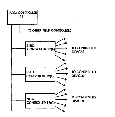
FIG. 1, the distributed control system 10 in~ludes an area controller 11 and one or more field
controUers 12(1) through 12(F) (generally identified by reference numeral 12(f)), which may be
conveniently u~lerconnc~,led by a network 13 or other communications arran~e.lle,.l. The area
10 colltloUer I 1 . ~ t ,:,~c overall control of the industrial operation under control, or a portion thereof,
thereby ..., ~ ng overall control of the m~nlJf~ lring process. Each of the field controllers 12(f),
under control ofthe area controller, controls a portion of the plant, and in particular controls specific
5 ofthe plant, such as specific m~hines (not shown) in a m~mJf~cturing operation or specific
valves and reaction ch~..bc.s in a chemic~l processing plant. In addition, each field controller 12(f)
15 will receive status i~lfo~ ~ion pref~ ly from sensors (also not shown) in its ~csigned portion of the
plant which irx~e~heir status in the process under control. Depending on the control infollllalion
and ope.alional pal~llelers provided by the area controller 11 to a field controller 12(f), the field
controller 12(f) may, in r~syonse to the status information it receives from the sensors coMe~,lcd
thereto, control the machines to perform selected operations as determined by their pro~.... .;ng
In addition, the field controller 12(f) may notify the area controller 11 if the status i.~.. lalion
indicates that operations in its area is outside of selected operational ranges, and the area controller
11 may initiate cG..~,cti~e procedures in conne~t;on therewith.
FIGs. 2A and 2B tog~,LLer depict a functional block diagrarn of a field controller 12(f) useful
in the distributed control system 10. With reference initially to FIG. 2A, the field controller 12(f)
25 colll~ s a plurality of modllles, in~lurling a processor module 20 and one or more eyp~n~ion
modules 21(1) through 21(E) (generally identified by l.,fere.lce numeral 21(e)) whose ele~ ical
features are depicted in FIGs. 2A and 2B. Structural features of one embodiment of the field
21 8759rJ
controller 12(f) will be descl;bed below in connect;on with FIGS. 3 through 6B, and structural
features of a second embodiment of the field controller 12(f) will be described below in conn~l;on
with FIGS. 7 through 10B. As will be desc~il,ed below, the modules 20 and 21(e) each have external
conl-~cl;on~ which are pos;liol-ed and configured to enable them to be connected together in a
5 relatively ~l..pa~l manner. In addition, the modules 20 and 21(e) provide external int~ c~ to
control devices in the factory envi.onl~lent. The entire field controller, COlllplisil g the processor
module 20, one or more e,~,dnaion modules 21(e), along with power supply and input/output devices
which may be conn~cted thereto (not shown) provides a very compact yet computationally-powerful
and easily l.~ n~ble package, which is convenient and quite useful in an industrial envi.~)n,..c~
The processor module 20 comprises a processor submodule 22 and a local communications
submodule 23. The processor submodule 22, in turn, include5 a central processor unit 24, a read-
only memory 25 and a main random-access memory 26, all of which are coMected to a bus seg...~ ..l
27, and may also include other components as described below. The central processor unit 24 is
pl~,f~.ably in the form of a microprocessor. The read-only memory 2S provides non-volatile storage
15 which may be used for, for ~.~..ple, a BIOS (basic input/output system) portion of the operating
system program that ~ls the central processor unit 24, and may also provide storage for certain
other fixed opc.~ting info. lllalion. The main random-access memory 26, which may consist of one
or more conventional DRAM (dynamic random-access memory) chips, provides storage for programs
and data which may be down-loaded by the area controller 11 to enable the field controller 12(f) to
20 operate, data received from the controlled devices and sensors controlled by the field controller 12(f),
u~l..~ion plu~d by the central processor unit 24, and status information which may be retained
for ll~n~.. C-;on to the area controller. In one emboflim~nt~ the bus segllle.l~ 27 confol.. s to the well-
known ISA bus spe,cification, which defines a specification for buses used in personal computers,
although it will be appreciated that bus segment 27 may conform to other multi-drop bus
25 specific~tio~s
In addition to components 24 through 26, the processor sub-module 22 may include one or
more external communication ports (generally identified by leference numeral 30) for, for example,
2 1 87590
f?.cilitqting cotnm~)niC-qtions with the area controller 11, devices such as light f~ l;n8 diodes,
g~h,.dly i~e~tified by ~f. rence numeral 31, for providing visual status indic~fions, and devices for
rece~ving local control input, such as a reset signal provided by a reset button 32. The p,ocess~r sub-
module 22 may also include devices such as spealcers (not shown) for~ene.~ g audible alann or
5 status ;..-~ ~;ons All ofthese Pll~n, ,~ are indicated as being cotlnted to t~he ISA bus SP~8.... n~ 27
over an interface 33.
Wllile the bus sc~..,e~,~ 27 has been des~ ~;bed as cGnfollluny to the ISA bus sperific~q~tion~ it
will be apprecialed that other types of busses may be used for the bus sc~, en~ 27. P.efe~ably, the
bus s~3rn~ont 27 will be in the forrn of a "multi-drop" bus, that is, it will fq-cilitqte the intc,. ~nne~-(;on
10 of more than two devices to f~r.ilit~q~te the transfer data and status information the.t~l"ong In
addition, the bus se~ment 27 will preferably provide an interrupt facility, by which the central
p,~ess~r unit 24 can receive interrupt requests from other devices that are cGIù~ecLed to the bus to
notify it of conditions that may occur on an asynchronous or non-periodic basis which require
servicing by the central processor unit 24, as will be desc, ;bed below.
The l.. v~sjor sub-module 22 in one embodiment is p. ~fe. ably in the form of a single module
having a form factor defined by the PCMCIA ("Personal Computer Memory Card International
~cc~qtion") :,~nd~d, with ~im.on~ionc generally 3 3/8 inches long by 2 1/8 inches wide, by 1/4 inch
deep, and having an ISA bus interface preferably along one of its long edges. A suitable processor
sub-module 22 is currently sold by S-MOS Corporation as a model CARDIOTM 486 processor
module, which provides the above-identified components and inrhllling an 80486-class
f~,l optocessor as the central processor unit.
The local comm..nications sub-module 23 also includes a bus se~ 40 and a plurality of
PCMCIA interfaces 41(1) through 41(P) (~enerally idrntified by ,eference numeral 41(p)), which are
ulte~c~nn~ by an interface controller chip 42. The bus seg...~n~ 40 of the local cornm~n c~tio~lc
submodule 23 is logically similar to the bus seg.. Pn- 27 of the processor sub-module 22; that is, in
the embodiment in which the processor submodule's bus sç~rnrnt 27 collfo""s to the ISA bus
~. ;l~r~;on, the local comm~ - ~ f :r sub-module's bus segment 40 will also conform to the ISA bus
21 875~0
;on Ttle local coQlm~Qicatiorls sub-module's bus segment 40 co~tn~clc to the processor sub-
module's bus s~n~ut 2~ through a downstream connector 43.
The interface controller chip 42 provides a connt~ion from the bus s~ 40 to the
PCMCLA ult~.f~ces 41(p). Each PCMCIA interface in turn, provides a cann~ ;on to a PCMCLA
5 device, that is, a device which confol-lls to the elc~,l,ical interface defined by the PCMCIA
specification id- .n;~ above. The PCMCIA specific~tion defines, in ~rlitjol- to the PCMCIA fonn
factor d~.l~ above, an electrical interface which is esse~ti~lly a point-to-point bus, that is, a bus
which ir.tc~cGnnP~s only two devices. (This is in contrast to the ISA bus specific~tion which, as
described above, defines a multi-drop bus, which can interconne~l more than two devices.) Each
10 PCMCIA interface 41(p~ in~lud~s an interface connector 44(p) which co~np~ls to the interfacc
CO~ q~ chip 42, an in~e.race card 45(p), and an external il~l~,.Lce 46(p) which provides an illt~,.Çacc
to a controlled device (not shown) which may be located in the industrial en~,;.oru"cut, as des~,ril~
above. The interface card 45(p) is preferably constructed in the PCMCIA forrn-factor as desc,ibed
above, and provides circuitry which converts between PCMCIA signals provided by the intelrace
15 controller chip 42 and signals L,~n~m;lled to and received from the controlled device or sensor
.coMected to the card 4S(p). It will be appreciated that the particular circuitry provided in each
i.,le.r~ce card 45(p) will generally depend on the particular controlled device or sensor to which the
card 45(p) is connP~Ied
As des~ribcd above, the p. ~sor module 20 provides an interface to two controlled devices
70 through the local comrnunications sub-module 23. To increase the number of devices which may be
controlled by the local controller, one or more e~p~ns;on modules 21(e) may be connected to the
processor module 20. In particular, the local cornmunic~tion~ sub-module 23, in addition to
providing a conn~l~43 to the p-oc~r module 22, also provides an up~lrea l. connector 47, which
may be connc.Led to an expansion module 21(1), as shown in FIG. 2.
'5 llle ~ ?'-' 01l module, the physical structure of which will be desc r;l~ed below in cGnnc~l;on
with FIGS. 3, 6A and 6B, is electrically and logically similar to the local co-rmnnic2tions sub-module
23. That is, it is provided with a dowr~ream conllector S0, a bus segment 51, an up~ l conn~ctQr
21 87590
52, an interfacc controller chip S3 and a plurality of PCMCIA interfaces 54(1) through 54(p,)
~enerally iden~fied by refe~.lce numeral 54(p~)) which include an interface connector 55(p) which
~ to the interface controller chip S3, an interface card 56(p), and an external in~e~ e 57(p)
which provides an u~lerf~ce to a co.lt.ollod device (not shown) which may be located in the industrial
S envu on ll~4 as d~c.~d above. In one embodiment, the maximum number of PCMCIA interfaces
54~p,) that may be coMected in an expansion controller co, r~s~onds to the number of PCMCIA
interfaces 41(p) which can be connecled in the processor sub-module 20 is two, but it will be
appf~;at~ that an ~ n~ on module 21 (e) may provide more or fewer interfaces than the processor
module 20
10The downstrearn connector 50 of the first expansion module 21(1) connects to the external
connector 47 of the processor module 20, to connect the bus seg~,.ent 51 of the first e~nsicn
module 21(1) to the bus _C;~ t 40 of the local çon m~ ons sub-module 23, and thus to f~rilit~te
the transfer of si~nals from the processor sub-module 22 to the first expansion module 21(1) The
bus segrn~nt 51 couples the signals from the dO~llaLl`~ll connector 50 to the upa~eal~l Connff~tor
1552 for transfer to a further expansion module 21(2), if one is provided in the field controller 12(f).
As in the local Gom~lnic~tionc sub-module 23, the interface controller chip 53 couples signals
between the bus se~ment 51 and the PCMCIA interfaces 54(p,) which are provided in the first
expansion module 21(1)
As noted above, the e~p~n~icn modules 21(e) are all electrically sirnilar (and are similar to the
~0local communications sub-module 23 as described above) Accordingly, for each e~ C;on module
21(e) after the first, the res;~ecli~e downstream connector 50(e) will connect to the up~L.ean,
connector 50(e-1~ of the p. ,ceding expansion module 21(e-1) in the series, and the up~ea.~.
connector 50(e) will t,o~mecL to the do~~ lea.ll connector SO(e+l) ofthe next expansion module
21 (e+l ) in the series, with the module's bus segment 51 (e) coupling signals between the do~nslre~l
5connector 50(e) and the upslrean. connector 52(e) The interface controller chip 53(e) in the
respective ~ n~;on module 21(e) co"n~i to the bus segment 51 and the PCMCL~ interfaces 54(p,)
allowing the exr~nsiQn module 21 (e) to connect to a number of controlled devices over re;,~,e~,live
21 87590
-10-
PCMCIA illt~Lcc,s (not shown). Since for each G,~,ana;on module 21(e) the bus se y~ey~ls 27... 40...
51(e), i,lte.co"hP~,~ed by re~c~ ve connectors 43, 47, 50(1), 52(1), 50(e), 52(e), provide a
co~tin~o~C path for carrying data and control signals from the central plooessor unit 24 of the
processor sub-module 22 to the l~e~ e local comm..nications sub-module 23 and e-l,~s;~n
5 module 21(e), the central processor unit 24 is able to control the controlled device(s) through the
PCMCIA ;- ~tf r-~ 45(p) (in the case of a controlled device connected to the local cQmmw - hgnc
sub-module 23) or 54~p,) ~m the case of a controlled device ~ neele~ to an ~AnCion module 21(c).
As noted above, the expansion modules 21(e) and local communications sub-module 23 are
all electrically similar. The field controller 12(f) further includes a module selection ~lAn8~ . e~lt
10 which will-be dese,il~ in c~ le~ion with FIG. 2B whereby the processor sub-module 22 can select
which of the local comm~nications sub-module 23 or expansion module 21(e) is to receive signals
transmitted by it (that is, the processor sub-module 22) on the res~e~ e bus se~ n~s 2?... 40...
51(e), or which ofthe local c~mmunic~tions su~module 23 or expansion module 21(e) is to llan~s
signals to it (that is, the plocessor sub-module 22) onto the reape~ e bus se~..P ~tS 27.. . 40... 51(e).
Wlth ~f~,.,ce to FIG. 2B, in c~ ;on with the module selection a lange.lle.1t, the p-ocessor sub-
module æ ~ S a plurality of MOD SEL module selection signals for trAncmicci~n through a set
of conn~ o~ 28(A) through 28(D), with p.ocessor sub-module 22 controlling the pattern of asserted
and negated signals so as to select one of the local communications sub-module 23 or an e~An~;~n
module 21(e). Each of the local communications sub-module 23 and the expansion modules 21(e),
in turn, innludes a sPlecl;on signal select and rotation network 29(0) through 29(3) that (a) selects
a predetermined pattern of the signals for use in controllin~ selection of the local communi~qtionS
sub-module 23 and expqnsion modules 21(e), and (b) rotates the signal pattern for tlAn~ s~;~n to
the next local comn~ nications sub-module 23 or expansion module 21(e) in the series ofthe local
comm..nications sub-module 23 or expansion modules 21(e).
In the embodiment depicted in FIG. 2B, in which one local commllnic~qtions sub-module 23
and three ~Amion modules 21(e) are provided, the four MOD SEL module selection signals are
provided, labeled A0, B0, C0 and D0. In that embodiment, the local colTlmunicAtionc sub-module
21 87590
23, which is conn~cted directly to the processor sub-module 22, receives the MOD SEL module
selection signals A0, B0, C0 and D0, and decodes the A0 and B0 si~nals. If the processor sub-
module 22 is asj~,.lillg both the MOD SEL module selection signals A0 and B0, the local
c~mm--nications sub-module 23 will detennine that it is the NsPlected" module for cc ~ ons
5 over the bus segment 40. In any case, the local comm~niC~tiollc sub-module 23 will rotate the MOD
SEL module 5- ~e~(;on signals so that the signals A0, B0, C0 and D0 will be coupled to the e~pqnQ;cn
module 21(1) as the signals Dl, A1, B1 and Cl.
The expansion module 21(1) uses the module selection signals A1 and B1 to determine
whether it is the Nselected" module for communications over the bus segment 51(1). As desc,il,ed
10 above, the module selection signals A1 and Bl as received by the expansion module 21(1), in turn,
correspond to MOD SEL module selection signals B0 and C0, respeaively, as generated by the
p,oc~or sub-module 22. Accordingly, if the processor sub-module 22 asserts the signals B0 and
C0, the expansion module 21(1) will determine that it is the "selected" module for cornmllnicqtions
over the bus se~".e ~ 51(1). In any case, the expansion module 21(1) will rotate the MOD SEL
15 module seleaion signals so that the signals Al, B1, C1 and D1 will be coupled to the expansion
modu~e 21(2) as the signals D2, A2, B2 and C2.
Similarly, the expansion module 21(2) uses the module selection signals A2 and B2 to
det~..l..ne whether it is the "selected" module for communications over the bus se~".~nt 51(2). As
desc,ilJed above, the module ~l~ion signals A2 and B2 as received by the e~cpqncion module 21(2),
in tum, ~s--es~nd to MOD SEL module selection signals C0 and D0, res~e~,Li~ely, as generated by
the proce3sor sub-module 22. Accordingly, if the processor sub-module 22 asserts the signals C0
and D0, the ~xpqncion module 21(2) will determine that it is the Nselected" module for
c~mml -q~isnQ over'the bus segment 51(2). In any case, the expansion module 21(2) will rotate the
module selection signals so that the signals A2, B2, C2 and D2 will be coupled to the PYpqnQion
module 21(3) as the signals D3, A3, B3 and C3.
Finally, the eAI,ans;on module 21(3) uses the module selection signals A3 and B3 to detennin
whether it is the "selected" module for comm~nicvqtions over the bus segment 51(3). As descnbed
21 87590
above, the module selection signals A3 and B3 as received by the expansion module 21(3), in turn,
correspond to MOD SEL module selection signals D0 and A0, respe~ vely, as generated by the
yluc~r sub-module 22. Accoidingly, if the processor sub-module 22 asserts the signals D0 and
A0, the eYp~n~;on module 21(3) will determine that it is the "selected" module for comm~nic~ions
5 over the bus s~gn~ 51(3).
Urhile FIG. 2B depicts selection of the local communications sub-module 23 or one of three
e,~,dr~on mo~ Ps 21(1) through 21(3) using four MOD SEL module selection signals A0, B0, C0
and D0 as ge~ ated by the processor sub-module 22, by means of selection networks 29(0) through
29(3) as depicted in the FIG., it will be app.~;aled that, by suitable modification which will be readily
10 appdr~ ,lt to those skilled in the art, module selection signals and selection networks may be provided
by which more or fewer modules may be selected.
The field controller 12(f) which is logically depicted in FIGs. 2A and 2B, provides an
~cl.it~ lre which may be conveniently imrl~m~n~ed in a compact package which is readily installable
and m~int~in~ble in a factory environment. One embodiment of such an impl~m~ont~tion will be
15 described in co....e~ n with FIGS. 3 through 6B, and a second embodiment will be described in
connection with FIGs. 7 through 10B. The embodiment depicted in FIGs. 3 through 6B may be
m-)llnted on, for example, a vertical support such as a wall, with the processor module 20 and each
~p~ncioll module 21(e) being generally configured so that, when an exr~nsio~ module is added to
the field controller 12(f), it will be connected to the processor module 20 or to previously-provided
20 e~ ;on modules so as to extend the field controller 12(f) in a direction which is generally parallel
to a plane of the vertical support. The embodiment depicted in FIGs. 7 through 10B may also be
mounted on a vertical support, but the processor module 20 and expansion modules 21(e) are
g~n~.dly configured so that, when an expansion module 21(e) is added to the field controller, it will
be connected to the processor module 20 or to previously-provided expansion modules so as to
25 extend the field controller 12(f) in a direction which is generally transverse to a plane of the vertical
support.
21 875qO
-13-
With refere. ce initially to FIGS. 3 and 4, those FIGs. depict pe.spe~ e views of field
controllers 12(f~) and 12(fB) from two diverse orientations, with FIG. 3 particularly dep.clu1g the
processor module 20 component of the field controller 12(f~) and FIG. 4 particularly d~ tin~ an
e~ fi- ~n module 21(e) of field controller 12(f8). The field controllers 12(f".) and 12(fB) d~ ed
5 in FIGS. 3 and 4 are generally similar except that field controller 12(f~) in~ludes a processor module
20 and one ~~ o~ module 21(1), whereas field controller 12(fB) in~ludes a processor module 20
and three e~ n~;orl modules 21(1) through 21(3). (Since the field controllers 12(f~) and Seld
controller 12(fB) are otherwise similar, they will be generally identified here.na~ler by r~fe~ence
numeral 12(f).) FIGS. 5A and 5B depict opposing sides of the physical structure 60 of an ele~,l,onic
10 circuit useful in the processor module 20 and FIGS. 6A and 6B depict opposing sides the physical
structure 61 of an ele.,l,c ^ circuit useful in the expansion module 21(e). It will be app~oc;a~ed that
the processor module circuit structure 60 constitutes an impl~ al ;on of the circuit ele~ t~ of the
processor module 20 described above in connection with the schem~tic diagram in FIG. 2, and the
expansion module circuit structure 61 constitutes an impl~rn~nt~tion of the circuit ele.,~ la of an
15 e,~ ;on module 21(e) described above in conne~ion with the srhPm~tic diagrarn in FIG. 2.
~ lth ~ nce to FIGS. 3 through 6B, the field controller 12(f) includes a housing 65 having
a rear m~unting bracket 69 for mol ln~ing the field controller 12(f) onto a surface such as a wall or the
li;ke. The housing inrludes a left end cap 70 (shown in FIG. 3), a series of seg,..P nc 71(A) through
71(D) (g~,~e.olly idPntified by re~er~,nce numeral 71 (s)) and a right end cap 72. (FIG. 3 depicts only
se~... Pn-~ 71(A) and 71(B)), and FIG. 4 depicts all four segments 71(A) through 71(D)). The
seg,n 71(A) is ~: Pr.- O~ to fit the processor module circuit structure 60, and each of the other
s~ 71(B) through 71(D) is dimensioned to fit an expansion module circuit structure 61. Each
ofthe se~--- ~ 71(st CGI~lpl;S~S upper, lower, front and rear enclosure ele.,.e,-ts 73(s) through 76(s),
ely, (lower and rear enclosure elements 74(s) and 76(s) are not shown in the FIGS.) which
25 snap together laterally (that is, open-end to open-end) to, with the end caps, form col-ti~ous
elements of a continl-ous enclosure. Snap fastening ele ..enlç generally identified by refe.~,nce
numeral 77 are provided to fasten the seg...e .~s 71(s) and end caps 70 and 72 together.
21 87590
-14-
It will be appreciated from the description below that, in the embodiment depicted in FIGS.
3 and 4, the left end cap 70 may be provided integrally with the seg~..P ~ 71(A) for the processor
module circuit structure 60, whereas the right end cap is provided separately from any of the
s<~...e ~c 71(s) and added to the rightmos~ se~ This results from the fact that, in that
5 c ..1~~ are added to the right of the processor module seQ,- ~ .l 71(A). Since the left
end cap 70 will always be provided for the processor module se~ ,l, it is preferably provided
integrally with the seg~-e ~l 71(A).
As dcsc,ibed above, each segment 71(s) includes upper, lower, forward and rear ~nclosl.re
Fle~ tC 73(s) through 76(s), respectively, co~.lp.;a;ng the sidewalls for the seon~,( 71(s). The lower
10 and rear enclosure ele."cnts 75(s) and 76(s) are preferably generally planar FIP ~ lS, qlthou~h the
rear Pnrlos~re elP .,f l~c 76(s) may also be provided with a fastener to receive a conventional DIN
mo~ntin~ rail 77. The upper enclosure el~m~ntc 73(s) are preferably in the form of a finned heat sink
to fi ~ tqte ~icc;pzl;on of therrnal energy which will be generated by the ele~ un.c circuit ~le "~ .~c
which con~ained within the enclosure. The forward enclosure elem~ntc 75(s) for the reJ~,e~ e
15 s~ mS p,~fe.ably in~ludes a number of components, inclu~ing an access door 80(s) and a recess
82~s) (recess 82(D) is particularly shown in FIG 4) for receiving one or more external connectors
81(s)(A) and 81(s)(B). The access doors 80(s) are hinged at the top and open upwardly to provide
access to the ,~s~,e~ e modules 20 or 21 contained therein to facilitate insertion of col"ponenls or
removal for mq-intenqnce as described below. In addition, the access door 80(A) of the processor
20 module ~g,-~ t 71(A) includes a co~c.,lor for the external communication port 30, the visual status
in-l - "Ola 31 and reset button 32, and may also include connectors for audible alarm in~ic~q,tors (not
shown).
As describe'd above, the processor module seV",~nt 71(A) is preferably configured and
dimensioned to receive the processor module circuit structure 60 and each exrqnsicn module
2S segrn~ntC 71(B) through 71(D) is preferably configured and dimensioned to receive an eXpqnciQn
module circuit structure 61. The structure of the processor module circuit structure 60 useful in one
embodiment will be described in connection with FIGS. 5A and 5B, and the structure of the
21 87590
-15-
~.cp~ns;on module circuit structure useful in the sarne embodiment will be described in connecl;on
with FIGS. 6A and 6B. ~Ith reference initially to FIGS. 5A and 5B, the processor module circuit
structure 60 incl~ldes a circuit board 90 having mounted on one side thereof a con~ector 91 for
receiving the processor sub-module 22 and on the other side a connector 92 for receiving the
PCMCL~ interface cards 45(1) and 45(2). The bus seg,. e~ l 27 in the processor sub-module 22 is
internal to the p.ocessor sub-module itself, and is not depicted in FIGS. 5A and 5B. The circuit
board 90 will be provided with traces (not shown) that ele,~,ll;~lly interconnect the connectors 91 and
92 and an off-board connector 93 (shown particularly in FIG. 5B), to carry signals among the
pr~cessor su~module 22 and PCMCIA interface cards 45(1) and 45(2). It will be app.~,~.aled that
the conn~lor 91 and circuit board traces generally correspond to the connector 43 and bus sesrn~nt
40 d ~r ~ed in FIG. 2, and the connector 92 generally corresponds to the connectors 44(1) and 44(P)
shown in FIG. 2. In addition, the off-board connector 93 generally corresponds to the Up~
conne~,lor 47 in FIG. 2. Circuit board 90 is also provided with connectors and the like, generally
id- .~;r.C~ by refe;ence numeral 94, for connecting the serial port 30, visual status indicators 31 and
reset button 321Ocated on the access door 85(A), and for connecting the circuit board 90 to a power
~pply (not shown).
As shown in FIGS. 5A and 5B, the connectors 91 and 92 are configured so that the processor
sub-module n and PCMCIA interface cards 45(1) and 45(2) will be positioned generally parallel to
the circuit board 90 so as to provide a relatively thin package that may be conveniently positioned in
the seg~en~ 71(A) generally parallel to the left end cap 71 with the off-board connector 93 being
po~;tione~ toward the rear enclosure element 96(A). The off-board connector 93 corresponds to the
connector 47 (~IG. 2) and facilitates the connec~ion between the processor module 20 and an
e~l,a .- on module 2~(1). P-~,r~l~bly, the off-board co~-ector 93 provides pins and/or receptacles that
are oriented generally transversely to, and towards the right of (as shown in FIGS. 5A and 5B) the
plane of the circuit board 90.
Wlth l~ft.~nce to FIGS. 6A and 6B, the expansion module circuit structure 61 also incllldes
a circuit board 100 having mounted on one side thereof a connector 101 for receiving the PCMCIA
21 87590
-16~
interface cards S4(1) and 54(2), and in addition includes off-board connectors 102 and 103. The
co..nP~tor lOlis configured so that the PCMCIA interface cards 54(1) and 54(2) will be positioned
generally parallel to the circuit board 90 so as to provide a relatively thin pac~age that may be
comeniently p5;a ~iolle;l in a se,~ 71(s) (other than the se~ 71(A) for the processor module
5 20) with the plane of the circuit board 100 being generally parallel to the plane ofthe circuit board
90. Off board con~ or 102, which is situated on the left of (as shown in FIGS. 6A and 6B) circuit
board 100, includes pins and/or receptacles which are oriented generally transversely to the plane of
the circuit board 100, and which mate with corresponding elements of the off-board connector 93 of
the processor module circuit structure 90 ~FIGS. 5A and 5B).
Off-board connector 103, which is situated to the right of (as shown in FIGS. 6A and 6B)
circuit board 100 is similar to the off-board connector 93 of the processor sub-module, and also
provides pins and/or receptacles that are oriented generally transversely to the plane of the circuit
board 100. Since the off-board cQ~ e~,lor 103 is similar to off-board connector 93, and since the off-
board c4.-n~lor 102 will mate with the off-board coMector 93 of the processor module 22, the off-
board c~ ula 102 of each successive eYI~n~ion module 21(e8), 21(ec), .. , will also mate with the
off-board conne~ols 103 ofthe respective previous e~l.An~;on module 21(e~), 21(e8), ..., in the series
of expansion modules 21(e), thereby to accommodate addition of expansion modules as des~,.;bed
above. It will be appr~;ated that the off-board connector 102 effectively co~ ponds to the
do~..sL,ea,.l coMector 50 of expansion module 21(e) as des~l;bed above, and the off-board
conne~lor 103 effectively corresponds to its upsllealll connector 52. The bus seg.,.P"t 51 will
~nd to conn~ionc between the off-board co~ , a 102 and 103 on the circuit board as well
as to electrically-conduaive traces interconneçting the connectors 102/103 and the PCMCIA
co~n~ctor 101.
Returning to FIGS. 3 and 4, as noted above, the processor module circuit structure 60 and
the ~ ;;!n module circuit structure(s) 61 both snap into fesp,tc~ive se~,. ,P .ls 71(s) of the housing
65. Each aegrnent 71(s) is provided with snap r~ n~c 78 (shown in FIG. 4) to engage the
edges ofthe respe.,~i~e circuit boards 90 (in the processor module segtnent 71(A) and 100 (in the
21 87590
on module s~ nls 71(B) through 71(D). In addition, as shown particularly in FIG. 4, each
PCMCIA ult~Lce card 45(1y45(2) may be c~nnected to an external connector 81(s)(A) or 81(s)(B)
by means of wires, such as wires 84, eYt~ndin~ from the interface card, which may extend exteriorly
of the S~ through a slot 83(s) formed in the recess 82(s).
S Since the field controller 12(f) as described above in connection with FIGS. 2 through 6B is
modular, it provides a co...pa~ n~dblP easily~onstructed and easily-m~int~in~ble a~ g~ ~e~t
The field controlla 12(f) may be readily qcSPml~'c i by snapping the processor module circuit structure
60 (FIGS. 5A and 5B) in the segment 71(A) and any e,~pdrs;on module circuit structures 61 that may
be required for a particular field controller 12(fl in corresponding seg,nents 71(B), 71(C), and so
forth. The extemal connector 30, reset switch 32 and external in~licator 31 may be mounted on the
access door 75(A) of s~ enl 71(A), and the external connectors 81(s)(A)/81(s)(B) may be mounted
in the recesses 82(s) of the respective se~m~nts 71 (s) and connected to the PCMCIA interface cards
therein. Thereafter, the reil,e~ /e connectors 93 (of processor module circuit structure 60) and
coi nec~ol~ 102 and 103 (of expansion module circuit structure 61) will be in regis~ ion so that,
15 when the se~en~s are snapped together, the downstream connector 102 ofthe expansion module
rcuit structure 61 m a ~.~ 71(B), 71(C), 71(D), , will be in secure electrical contact with the
connector 93 of the processor module circuit structure 60 in seg.l,e.ll 71(A) or the up~lle~
~-ne~lor 103 of the expansion module circuit structure 61 in segrnPnt 71(B), 71(C), .... ARer the
last se~., .~ 71(s) has been added, the ri~ht end cap 72 may be snapped into place to complete the
20 ~nClQs~re for the field controller 12(f).
It will be appreciated that a field controller can be readily expanded in the field by simple
upgrading of the processor sub-module 22 and by the easy addition of expansion modules 21(e).
Addition of expansion modules 21(e) can be readily accomplished by ur,~"apping of the end cap 72
and snapping a new seg...~ .~ 71(S+I) onto the le~-most segment 71(S). Since the newly-added
seg,.. ~ 's off-board connector 102 is ensured to be in registration with the connector 103 of the
segrnent 71(S) onto which it is being mounted, the new segm~ont 71(S+1) is ensured to be properly
el3~,l-ically co--n~ to the segrnent 71(S) and to all ofthe seg-"e."s 71(A), .. , 71(S-I) do~lla~lealll
2187590
-18-
thaeo Since the PCMCIA inlc.race cards effectively communicate with the processor sub-module
22 over a bus c~.l.p.;~;ng a series of bus seg",.~ s, the PCMCIA interface cards conne~lcd to
particular controlled el~m~ ~ls in the factory environment can be placed in any se~ 71(s).
It will filrther he appre~,;~o~ that the field controller 12(f) can be readily serviced in the field.
5 The access doors 75(s) in particular of the respe~ /e se~ nlc 71(s) provide ready access to the
PCMCIA interface cards 45(p) and S6(p) for service. The processor sub-module 22, and the
PCMCIA interface cards can be individually removed and replaced in the field as nece5C~r in the
event of an upgrade or a m~lfiJnction through the access doors and without othe~wise requiring
~;~ac~...hly
As noted above, FIGs. 7 through IOB depict a second embodiment of the field controller
12(f), idPntifiPd herein by ~eÇe~ ~nce numeral 112(f), in which the p. ocessor module 20 and eyr~ncion
m~--lPs 21(e) are generally configured so that, when an expansion module 21(e) is added to the field
controller, it will be connected to the processor module 20 or to previously-provided e,~ans;on
modules so as to extend the field controller 12(f) in a direction which is generally transverse to a
plane ofthe vertical support. FIG 7 depicts a field controller 112(f) having a processor module 20.
(In the P .ll~;...~ .l de~l;l,ed in FIGs. 7 through IOB, the processor module 20 includes a processor
sub-module 22 and two local communication sub-modules, one of which co.l ~sponds to the local
comml r~isn su~module 23 depiaed in FIG 2A, and the second local cQmm..nication sub-module
co.lesponding to the first expansion module 21(1) depicted in FIG. 2A.) FIG. 8 depicts a field
controller 112(f)' having a p.~or module similar to the p.u~r module 20 of the field controller
d~.F--t~ in FIG. 7, and two ~-p~ ;on modules 21(e), which cû.l~spond to exp~nC;on modules 21(2)
and 21(3) deri ~ed in FIGS 2A and 2B.
Wlth l~f ,~.~e to FIG. 7, the field controller 112(f) depiaed in that FIG comprises a housing
120 having a rear support member 123 and a cover 124. The rear support member 123 inrludes
bracket 121 for molmtin~ on a surface such as a wall or the like In one particular embodiment, the
bracket 121 couples onto a conventional DIN rail idPntified by tference numeral 122, which, in turn,
21 87590
, 9
may be mounted on a surface (not shown), but it will be appreciated that other mollnting
,,lh~ge~,-.,.-Ls may be provided for mo~lnting the field controller 112(f).
As shown in FIG. 7, the rear support member 123 includes forwardly-eYt~nding base .llc."b~r
12S that inf~ludes a power connector, reset button and external connectors which are similar to the
S co"~ 5~on~ g . ~ c 31 and 81(s)(t) desc-il~ above in conne~l;on with the embodiment dep;~(ed
in FIGs 3 through 6B. The cover }24 includes a light e~ ;ng diode status display 126 which
comprises lenses for light ç.";~l;n~ diodes for providing visual information conce-,un~ the status of
the field controller 112(fJ, in particular whether the field controller 112(f) is powered-up and whether
it is functioning properly or requires servicing. In addition, the field controller 112(f) inrludes an
10 access door which provides external access to an interior connector corresponding to coMe~,lor 30
de~.,l,ed above in connection with the embodiment depicted in FIGS. 3 through 6B. As noted
above, the field controller 112(f) depicted in FIG. 7 include5 a single processor module circuit
structure 150, which, as will be described below in connection with FIGS. 9A and 9B, colllprises a
single circuit board having a processor sub-module 22 mounted on one side of the circuit board and
two PCMCIA illLel race cards 45(1) and 45(2) mounted on the opposing side of the circuit board, with
the planes of the processor sub-module 22 and PCMCIA interface cards being parallel to the plane
ofthe circuit board. The processor module circuit structure 150 is mounted interiorly of the housing
120, in particular being supported by the rear support member 123, with the rear support member 123
s~ppo,~g the processor module 20 so that the plane of its circuit board generally parallel to the rear
20 support and malntin~ surface on which the field controller 112(f) is mounted. Wires inte~connec~;ng
the respe~ te ~le.. ~c ofthe processor module circuit structure 150 and external connectors are
routed interiorly of the housing 120.
As descril~d above, FIG. 8 depicts a field controller 112(fl' having a processor module circuit
structure 150 similar to the processor module circuit structure I S0 of the field controller depicted in
25 FIG. 7, and two expansion module circuit structures 160, which correspond to expansion modules
21(2) and 21(3) depicted in FIGs 2A and 2B. With refe.ence to FIG. 8, the field controller 112(f)
depicted in that FIG. co,l,~"ises a housing 130 having a rear support l"~",~er 131, an intermediate
2 1 87590
-20-
,l,e."~,r 132 and a cover 133. The rear support member 131 includes a rear bracket 134 for
mounting on a surface such as a wall or the like. In one particular embodiment, the bracket 134
couples onto a conventional DIN rail idPntified by l~fe.ence numeral 135, which, in turn, may be
mo~mt~d on a surface (not shown), but it will be appreciated that other mounting a~ar~ge~"~ s may
be provided for mo-lnting the field controller 112(fl'.
~s shown in FIG. 8, the rear support member 131 includes forwardly-exten~in~g base member
136 that in~ludes a power connector, reset button and external connectors which are similar to the
Col 1~ ~nf~ 31 and 81 (s)(t) described above in conne~,lion with the embodiment depicted
in FIGs 3 through 6B. The ulLelllled;aLe member 132 is generally similar to the rear support member
123 ofthe field controller 112(fl (except that it does not provide the mounting bracket 121 provided
by rear support member 123), and provides a forwardly-extending base l"e.,lbcr 137 that, in a manner
similar to base l,.e.l.ber 125 (FIG. 7), provides connectors and a reset button. The rear support
member 131 is generally sirnilar to support member 123 of the field controller 112(fl depicted in FIG.
7, except that it is somewhat longer so that the base member 136 will extend forwardly beneath the
base member 137 ofthe inte.l,led;aLe member. The base ~.lelllbe.~ 137 and 136 are prefe.ably stepped
(that is, the forward surface of base member 136 is somewhat rearward of the forward surface of base
member 137) so that wires conne~(ed to the connectors of the respective base members 136 and 137
to provide for a relatively neat routing of the wires.
The cover 133 is generally similar to the cover 125 of the field controller 112(f) depicted in
FIG. 7. In particular, the cover 133 includes a light-elll;tling diode status display 140 which
cG",I";ses lenses for light e ,.;tl;.,g diodes for providing visual inforrnation concerning the status of
the field collt~ 112(f)', in particular whether the field controller 112(f)' is powered-up and whether
it is fimctioning properly or requires servicin~. In addition, the field controller 112(f)' includes an
access door which provides external access to an interior connector corresponding to connector 30
desc,il,ed above in coMe.,lion with the embodiment depicted in FIGS. 3 through 6B. As noted
above, the Seld controller 112(f)' depicted in FIG. 7 includes a single processor module 20 and one
or more .~ An~,~on modules 21 (e). The processor module circuit structure 150 used in field controller
21875~0
112(f)' c~ onds to the module to be described below in connection with FIGS. 9A and 9B, and
the e~ on modlllPs 21(e) will be des";l~ed below in coMection with FIGS. 10A and 10B. As
with the p,~ss~r module circuit structure 150 used in the field controller 120, the process~r module
circuit structure used in field controller 112(f)' cG~ Jl;3es a single circuit board having a p~ucessor
sub-module 22 molmt~ on one side ofthe circuit board and two PCMCIA interface cards 45(1) and
45(2) mollnt~pd on the opposu~g side of the circuit board, with the planes of the processor sub-module
22 and PCMCIA interface cards being parallel to the plane of the circuit board. Similarly, each
e~cp~nciorl module circuit structure 160 comprises a single circuit board having two PCMCIA
interface cards 54(1) and 54(2) mounted on one side thereof, with the planes of the PCMCIA
interface cards being parallel to the plane of the circuit board. The processor module 20 and
e,~ on m~l-lPs 21(e) are all mounted interiorly of the housing 130, in particular being SUI~pOl ~cd
by the rear support Illll~CY 131, with the rear suppon member 131 supporting the processor module
circuit structure 150 and expansion module circuit structures 160 so that the planes of their circuit
board are generally parallel to the rear support and mounting surface on which the field controller
112(f)' is mollnted ~tres inLerconne~ 3 the respective elements of the processor module circuit
structure 150 and ~Ypqncion module circuit structures 160, and external connectors, are routed
interiorly of the hou5ing 130.
The structure of the processor module circuit structure 150 useful in connection with field
CO~ rS 112(~ and 112(f)' des~,libed above in connection with FIGS. 7 and 8 will be des~,libed in
oon~ ;on with FIGS. 9A and 9B, and the structure of the expansion module circuit structure 160
useful in the same embo~liment will be described in connection with FIGS. 10A and 10B. Wlth
l~,f.,r~.ce initially to FIGS. 9A and 9B, the processor module circuit structure I SO includes a circuit
board 151 having mounted on one side thereof a connector 152 for receiving the processor sub-
module 22 and on the other side a connector 153 for receiving the PCMCIA interface cards 45(1)
and 45(2). The bus se ~ 27 in the processor sub-module 22 is internal to the processor sub-
module itself, and is not dçFicted in FIGS. lOA and I OB. The circuit board 151 will be provided with
traces (not shown) that electrically interconnect the connectors 152 and 153 and an off-board
co.~ or 154 (shown particularly in FIG. 9A), to carry signals among the processor sub-module 22
2 1 87590
-22-
and PCMCIA i..l~.Lce cards 45(1) and 45(2). It will be appreciated that the connectsr 152 and
cirwit board traces generally correspond to the connector 43 and bus seg,~lc~-~ 40 depicted in FIG.
2A, and the conn~ or 153 generally col . ~sponds to the connectors 44(1) and 44(P) shown in FIG.
2. In ~dition~ the off-board connector 154 generally CGI I ~ onds to the Upal~ coi ne~Qr 47 in
5 FIG. 2A. Circuit board 151 is also provided with coMectors and the like, generally identified by
.~,f~.~,nce numeral 155, for corlnP~t;~g the serial port 30, visual status in~icators 31 and reset button
32 located on the access door 85(A), and for co.me~ g the circuit board 90 to a power supply (not
shown). In ad~lition~ the circuit board 151 supports light-Prnitting diodes 156 which register with
light e ~ g diode status display 126 or 137 to provide the above-described status in~ic~tion
As shown in FIGS. 9A and 9B, the connectors 151 and 152 are configured so that the
pr~sor sub-module 22 and PCMCIA interface cards 45(1) and 45(2) will be po~itioned generally
parallel to the circuit board 150 so as to provide a relatively thin pac~ee that may be conveniently
positioned in the se~ housing 120 or 130 as described above. The off-board connector 154
corresponds to the connector 47 (FIG. 2A) and facilitates the cor-ne~,(ion between the processor
module 20 and an expansion module 21(1). Preferably, the off-board connector 93 provides pins
- aud/or receptacles that are oriented generally transversely to the plane of the circuit board 151.
Wlth l~ference to FIGS. 6A and 6B, the expansion module circuit structure 160 also inrludes
a circuit board 161 having mounted on one side thereof a connector 162 for receiving the PCMCIA
interface cards 54(1) and 54(2), and in addition includes off-board connectors 163 and 164. The
conn~or 101is confi~.red so that the PCMCIA interface cards 54(1) and 54(2) will be positiorled
generally parallel to the circuit board 160. Off-board connector 163, which is situated on the le~ of
(as shown in FIGS. 10A and 10B) circuit board 161, includes pins and/or recept~nles which are
oriented generally ~ransversely to the plane of the circuit board 161, and which mate with
co.. ,~n~ Pl~ t~ ofthe off-board csn,-c~(or 154 ofthe processor module circuit structure 150
25 (FIGS. 9A and 9B).
Off-board corlnp~(or 164, which is situated to the right of (as shown in FIGS. 10A and 10B)
circuit board 160 is similar to the off-board connector 153 of the processor module circuit structure
21 8~590
and also provides pins and/or receptacles that are oriented generally transversely to the plane of the
circuit board 161. Since the off-board c4nl-e~(0r 164 is sirnilar to off-board connector 153, and since
the off-board connector 164 will mate with the off-board coMector 153 ofthe processor module
circuit structure 150, the off-board col-nectors 164 of each successive eYp~nC;~n module circuit
structure 160(eB), 21(ec), .. , will also mate with the off-board conne~lGla 163 of the lespe~ e
previous Pyp~n~ module circuit âtructure 160(eA), 21(e8), ..., in the senes of ~Yp~ncion module
circuit structures 161(e), thereby to ac~o,.,."od~le addition of e~,ar.a;on modules as desc,ibed above.
It ~,vill be app~c~,.ated that the off-board connector 163 effectively co,responds to the dov~llal~
connector 50 of e~ ncion module 21(e) as described above, and the off-board connector 164
10 effectively corresponds to its upal~ea-.l connector 52. The bus se~ ,nt 51 will col~spond to
connections between the off-board connectors 163 and 164 on the circuit board as well as to
electrically-corductive traces interconnecting the connectors 163/164 and the PCMCIA coMector
162.
While the invention has been described in connection with use of a processor sub-module 22
15 and u~t~.Lce cards having respe~ /e characteristics conforming to the PCMCIA specification, such
a~s the form factor and ~in the case of the interface cards) electrical interface specification, it will be
appreciated that the elements may have other forrn factors and interface specifi~tions. It is
preferable, ho~ er, that the CIC~..C~t5 have generally the sarne form factors, and be p.eft,.dbly
relatively thin so that the s~g,..~ 71(s) may be relatively thin f~ciiit~ting relatively tight pac~ing
In ~ ;tion, will be prefe.dble that any bus co.,.pl;s;ng bus se i.. ei-~s 27, 40, and 51 be a multi-drop
bus so that the PCMCIA interface cards for the various controlled devices can be col-n~cted
anywhere along the bus.
In ~ition, while the new field controller 12(f) (as well as field controllers 112(f) and 112(f))
has been des~ ed as opc.dting in a distributed control system 10 under control of an area controller
25 11, it will be appreciated that, dep-n~linQ on the particular applic~tion, area controller may not be
no~y and the field controller may operate independently. In addition, it will be app,cciated that
21 875~0
-24-
a variety of devices may be controlled by a field controller as desc, ibcd herein, in~luding other field
controllers.
The foregoing dexl;~Jtion has been lirnited to a specific embodiment of this invention. It will
be app;~ t, however, that various variations and modifications may be made to the invention, with
5 the a~a; ..,. Q~ of some or all of the advantages of the invention. It is the object of the appended
claims to cover these and such other variations and modifications as come within the true spirit and
scope of the invention.
What is claimed as new and desired to be secured by Letters Patent of the United States is: