Note: Descriptions are shown in the official language in which they were submitted.
~vo9snss68 21 87889 r~ 6~
--1--
LIG~T ~ DEVIC~ ~VING A ~TRIl~
Dlzn ~RON ACID ~--T~
Ba~kuL r A of the Invention
Field of the InventiQn
This invention relates to light modulating devices
(e.g., a polymer-dispersed liguid crystal device
hereinafter referred to as a "PDLC device").
10 Descri~tion of the Related Art
Various types of light modulating devices are
known. One type is the so-called PDLC device that
1 nrll-Aoc an electrically responsive liquid crystal
layer in which liquid crystal droplets are dispersed
15 th~uuyllvuL a polymer matrix. One way to prepare the
liquid crystal layer is by ~- ` inin~ the liguid crystal
material with a polymerizable matrix ~L~=uu-au- and then
subjecting the mixture to polymerization conditions.
Polymerization causes phase separation of the liquid
20 crystal material, resulting in the formation of liquid
crystal droplets dispersed U~ UUL the polymerized
matrix .
PDLC devices are tr~n~ ront in the absence of an
electric field due to light scattering and become
25 L~la~ upon application of the field. Reverse
mode PDLC devices are also known. These devices are
trar.~ r.:..L in the absence of an electrlc field and
become translucent upon application of the field.
Various PDLC matrices are known. They include the
30 polymerization products of epoxy, isocyanate, and
certain photo-curable vinyl -- - a (e . g ., acrylates
or the reaction product of a multi-functional thiol
with a multi-fllnrtic n~l acrylate or a multi-fllnr~io
allyl) .
During manufacture of the PDLC device, the liquid
crystal layer typically is placed in contact with one
: - j
W0 95/29968 ' ~ ~ ~ 7 8 8 9 r~ 6~
--2--
.
or more thin film eieu-~ udefi and then laminated between
two rigid protective sheetfi, e.g., glass sheetfi.
During lamination, the fiheets can be distorted by the
temperaturefi and ~lefit~uL~:fi afisociated with the
5 lamination procefifi. At the r~nrl~ inn of lamination,
the ~lL~2DDU~e: ifi relieved and the t~ LuLe is
reduced, allowing the distortions to relax. This
relaxation subfiec~uently D~L~SD~6 the liquid cryfital
layer. If the cohefiive l,~L~IIyL~- of the lic~uid cryfital
10 layer and/or the adhefiion of the liquid crystal layer
to the electrodefi ifi not fiuf f iciently high! thè stress
will cause the liquid crystal layer to fiplit apart
cohefiively and/or ~ lAminAte from the electrode.
One convenient way to characterize the resifitance
15 of a film to r~ nAtion or cohesive failure ifi to
measure itfi T-peel r~L~ h. A film with a higher T-
peel fitrength will be much leE B likely to d~l A'mi nAte or
cohesively fail during manufacture.
~aa~V of th~ Invention
In a first aspect, the invéntion features an
optically responsive film that inrl~ liquid~ crystal
difipersed in a polymer matrix that ifi the reaction
produût of (1) one or more poiymerizable matrix
reactants other than an acid reactant and (2) at least
25 one acid reactant copolymerizable with the one or more
matrix reactants in an amount sufficient to enhance t~ e
T-peel strength of the film (-eafiured according to ~est
ELuceduL~ A, ~a~) by a factor of at least 2 relative
to the fiame film yLt~aLtd in the absence of the acid
3 0 reactant .
As used herein, "acid reactant" refers to a
copolymerizable species provided with one or more
groupfi ciassified as Lewis acidfi.
"Polymerizable matrix reactant" refers to a
35 monomer, oligomer, or combination thereof that react,
along with the acid reactant (e. g., via a chain growth
,
,. , ~
WO95/29968 I~~ 1l3~
2~ 87889
--3--
or step growth - AniP"', or combination thereof), to
form the polymer matrix.
"The same film prepared in the absence of the acid
reactant" refers to a film ~.epdlèd without the acid
5 reactant but using the same matrix reactants and
initiator and/or catalyst as the claimed film in which
(a) the weight to weight ratio of individual matrix
reactants to each other t~Ps~ nq a composition having
more than one matrix reactant) is the same as in the
10 claimed film, (b) the weight to weight ratio of the sum
total of all the matrix reactants to the initiator
and/or catalyst is the same as the weight to weight
ratio of the sum total of all the matrix reactants plus
the acid reactant to the initiator and/or catalyst in
15 the claimed film, (c) the weight to weight ratio of the
sum total of all the matrix reactants plus initiator
and/or catalyst to liquid crystal is the same as the
weight to weight ratio of the sum total of all the
matrix reactants plus acid reactant plus initiator
20 and/or catalyst to liquid crystal in the claimed film,
and (d) the f ilm is ~L e~aréd under substantially the
same process conditions (e.g., t~ ~ItU~ and light
intensity) as the claimed f ilm .
In preferred ~mho~ s, the amount of the acid
25 reactant is chosen to enhance the T-peel r~LLelly~l by a
factor of at least three. The amount of the acid
reactant preferably ranges from about 1 to about 30
weight percent (based upon the total weight of matrix
reactants plus initiator and/or catalyst), more
30 preferably from about 2 to about 15 weight percent.
Preferably, the acid reactant is a protic acid
reactant having one or more acidic IIY~L oS~êns . The
protic acid reactant is preferably used in an amount
sufficient to yield a polymer matrix having from about
35 0.01 to about 0.4 weight percent acidic IIYdLOYe~
(based upon the total weight of matrix reactants plus
W095/29968 2~ 87 P~89 P~ 5 ~D6~
- _4_
initiator and/or catalyst), more preferably from about
0. 03 to about 0 . 2 weight percent. As an example,
acrylic acid (moiecular weight = 72 g/mol) has one
acidic l-ydLu~ (molecular weight = 1 g/mol) and, if
5 used at 18 weight percent, would provide 0. 25 weight
percent acidic l~YdLUY~nL~. ~ACidiC IIYdLUS~ CI~ are
labile 1IYdL~ from ~ having p~Ca's preferably
less than or equal to 5.
Examples of preferred acid reactants (all of which
10 are protic acid reactants) include ulll.aLuLated
carboxylic acids (e.g., acrylic acid and methacrylic
acid), mono-esters of u~-~,aLuLated dicarboxylic acids,
amine-functional carboxylic acids, hydroxy-functional
carboxylic acids, mercapto-functional carboxylic
15 acids, and sulfonic acids. ~
r ~ ~c of pref erred matrix reactants include
mono- or multi-functional enes (e.g., vinyl ethers,
acrylates, and/or methacrylates), thiols, silicon
hydrides, alcohols, epoxies, isocyanates, amines, or
20 combinations thereof. A "multi-functional" reactant
contains two or more groups that participate in the
polymerization reaction, whereas a "mono-functional"
reactant c~nt~ i nc only one such group . An "ene" is a
reactant having a polymerizable carbon-carbon double
25 bond. A "multi-functional ene" is an ene having two or
more polymerizable caL~c". ._aLLull double bonds.
In one preferred ~"ho~ , the matrix reactant
is a multi- and/or mono-functional ene (e.g., an
acrylate, methacrylate, vinyl ether, or combination
30 thereof) and the acid reactant includes an u..~aLuL~ted
carboxylic acid.
In a second aspect, the invention f eatures an
optically responsive film that incl~ c liquid crysta
dispersed in a polymer matrix that is the reaction
35 product of (1) one or ~ore pol-ymerizable matrix
reactants other than an acid reactant and (2) at least
~ . .
.
., ~ , ~ ~
wo 9sl29968 2 1 8 7 8 8 9 ~ 6~
--5--
one acid reactant copolymerizable with the one or more
matrix r~'ACt~ntC in an amount ranging from about 1 to
about 30 weight percent (and preferably from about 2 to
about 15 weight percent).
In a third aspect, the invention features an
optically responsive f ilm that ; nrl~ liquid crystal
dispersed in a polymer matriY that is the reaction
product of (1) one or more polymerizable matriY
reactants other than an acid reactant and (2 ) at least
10 one protic acid reactant copolymerizable with the one
or more matriY reactants in an amount suf f icient to
yield a polymer matriY having from about 0 . 01 to about
0.4 weight percent acidic I~YdLUY~ S (based upon the
total weight of matriY reactants plu5 initiator and/or
15 catalyst), and preferably from about 0.03 to about 0.2
weight percent.
The invention further features a light modulating
film that inr~ the abu~_ de~- ~ibed optically
responsive films to which an electric field is applied
20 through a pair of ele~ ~Lodes.
The invention provides optically responsive films
exhibiting; uv=d T-peel ~LeIIY~I as a result of
copolymerizing an acid reactant into the polymer
matriY. As a result, the films resist spl it~in~ apart
25 when electrical contact is made to the ele. Ludes
and/or during manufacture of the light modulating film.
other f eatures and advantages of the invention
will be ~ aI~:.,L from the following description of the
preferred ~ s thereof, and from the claims.
Brief Descrit)tion of the Drawin~s
The invention will be more fully understood with
reference to the following drawings in which:
FIG. 1 is a schematic view, partially in cross-
section, of a light modulating device according to the
3 5 invention .
wo 9s/29s68 2 ~ 8 7 8 8 ~ l3~
--6--
FIG. 2 is a ~;Luss-s~_Lional view of an extrusion
die useful in preparing film6=according to the
invention .
FIG. 3 is an enlarged cross-section view of the
5 die shown in FIG. 2.
FIG . 4 i6 an enlarged ~l .,ss-~ction view of an
alternative die useful in preparing f ilms according to
the invention.
De6criDtion of the Pref$rred F~h~
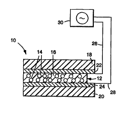
Referring to FIG. l, there i8 shown a light
modulating device lO comprising an optically responsive
film 12 having a multiplicity of discrete liguid
crystal droplets 14 having diameters in the range from
about 0.1 to 10 times the wavelength of light to be
15 scattered dispersed in a polymeric matrix 16.
Natrix 16 is the polymerization product of one or
more polymerizable matrix reactants other than an acid
reactant and one or more copolymerizable acid
reactants. The acid reactant ~nhAnr~c the T-peel
20 L~ yL~l of the optically responsive film (as measured
according to Te6t FLOCedUL-~ A~ inf~) by a factor of at
least 2 (and more preferably by a factor of at lea6t 3)
_ -- ed to the same film ~e~a~ed in the ab6ence of
the acid reactant ( a6 def ined in the Summary of the
25 Invention, above).
Examples of 6uitable acid reactants include protic
ncids such a6 ul-LaLuL-ted carboxylic acid6 (e.g.,
acrylic acid, methacrylic acid, crotonic acid, vinyl
acetic acid, itaconic acid, maleic acid, fumaric acid,
30 allylacetic acid, cinammic acid, and unsaturated acid-
terminated polyester oligomers); mono-ester6 of
dicarboxylic acids (e.g., - c_~er6 of maleic,
fumaric, and itaconic acid); amine-functional
carboxylic acids (e.g., Aminrh~n7~ic acid, 4-
35 i~m;nr-rh-,nylacetic acid, and variou6 amino acids);
hydroxy-fl-nr~ nAl carboxylic acid6 (e.g., 4-
wo 9S/29968 2 ~ 8 7 ~ ~ ~ P~ 1l.J ,,_ ~ l3~
--7--
11YdL UAY~ ZOiC acid); mercapto-functional carboxylic
acids (e.g., 3 ~ Lopropionic acid); sulfonic acids
(e.g., ~ydLu~-y~ nc~~ll fonic acid and sulfanilic
acid), and combinations thereof.
The total amount of acid reactant must be
sufficient to achieve the de8ired ~nh~- t. in T-peel
strength. However, where flexible films are desired
(e.g., in architectural and automotive applications),
the amount must not be high enough to cause the f ilm to
10 become hard and in~lexible. In addition, the amount
preferably is not high enough to cause the film to
possess a large amount of " y" (i.e., an increase
in off-state transmission relative to the trAn~ Eio~
before the film is powered). Memory is generally
15 largest the first time a film is switched on and off.
While the amount of acid reactant depends on the
particular acid reactant and the matrix reactants in
the poly-merizable mixture, in general the amount of
acid reactant ranges from about 1 to ~bout 30 weight
20 percent (and more preferably from about 2 to about 15
weight percent) based upon the total weight of matrix
reactants plus initiator and/or catalyst.
In the case of protic acid reactants, the amount
of acid reactant is preferably sufficient to yield a
polymer matrix having from about 0 . 01 to about 0 . 4
weight percent acidic l~Y-1LU~II8 (based upon the total
weight of matrix reactants plus initiator and/or
catalyst), more preferably from about 0. 03 to about 0. 2
weight percent.
Examples of materials with which the acid
reactants can be polymerized to form matrix 16 fall
into the following classes. Matrix reactants falling
within any particular class may be used in combination
- with each other or in combination with materials in the
35 other classes.
wosS/29968 ~ ~37~o~9 ~ 5~13c~
--8--
t 1) Cla58 I includes mono-functional and multi-
functional enes such as acrylates, methacrylates,
allyls, acrylamides, methacrylamides, vinyl silanes,
vinyl ethers, fumarates, maleates, or combinations
5 thereof.
Examples of mono-functional acrylates and
methacrylates include acrylate and methacrylate esters
of non-tertiary alkyl alcohols, the molecules of which
have from 1 to about 14 carbon atoms. Included within
lO this class of matrix reactants, are, for example,
isooctyl acrylate, isononyl acrylate, 2-ethylhexyl
acrylate, decyl acrylate, dodecyl acrylate, n-butyl
acrylate, heYyl acrylate, isooctyl - - ylate, and
lauryl methacrylate.
r 1PÇ: of multi-functional acrylates and
methacrylates include 1,6 hDYAnD~;r~ldiacrylate,
trimethylpropane triacrylate, propylene glycol
dimethacrylate, pentaerythritol tetraacrylate, and 1,2-
ethylene glycol diacrylate.
E 1 PS of mono- and multi-functional allyls
include mono-, dl-, and triallyl ~ '- and allyl
c _ '- containing an hydroxyl group reacted with a
mono- or multi-functional isocyanate, e.g., triallyl
isocyanurate, trimethylolpropane diallyl ether, allyl
25 benzene, allylcyc~ hpvAnD~ diallyldiphenylsilane, and
allyl-functional oligomers such as 9460 commercially
available from Mor -Polymer & Dajac Laboratories,
Inc ., Trevose , PA .
Examples of mono-functional acrylamides and
30 methacrylamides include N,N-dimethylacrylamide, N,N-
diethylacrylamide, N-dodecylmethacrylamide, and N-
ethylmethacrylamide .
Examples of multi-functional acrylamides and
methacrylamides include 1,6-h, ~llylpn~-h;P~A~rylamide~ -
35 N,N'-octamethylene-bisacrylamide, 1, 6-
WO 9S129968 r~ 6~
~1 87889
g
hexamethylPnPh; I thacrylamide, N,N-iso-valerylidene-
bis-methacrylamide, and m-xylene-bisacrylamide.
Examples of mono-functional vinyl silanes include
vinyltrimethylsilane, vinyltri- y~ilane,
5 vinyltris (trimethylsiloxy) silane, and l:i 1 r~YAnPS such as
that ~;ially available from Hiils America under the
trade designation "PS408. "
r 1PC of multi-functional vinyl silanes include
trivinylmethylsilane, 1,3-divinylteLL y1 t~ YAnC~,
10 1, 3 -divinyl-l, 3 -diphenyl-dimethyi rl i ci 1 ~YAnP ~
divinyldimethylsilane, divinyldiphenylsilane, 1,1,3,3-
tetravinyldimethyldisiloxane, tetravinylsilane, and
1,3,5,7-tetravinylteLL hylcyclotetrasiloxane.
Examples of suitable vinyl ethers include
15 l~ydLvAyLu~yl vinyl ether (HBVE, commercially available
from International Specialty Products, Wayne, NJ); 1,4-
cyc~ hPYAnP~li Lhanol divinyl ether (CHVE, commercially
llvailable from International Specialty Products, Wayne,
NJ); propenyl ether of propylene ~ILb.~ te (PEPC,
~;ially available from International Specialty
Products, Wayne, NJ); triethylene glycol divinyl ether
(DVE-3, commercially available from International
Specialty Products, Wayne, NJ); butanediol divinyl
ether ( .;ially available from BASF, Parsippany,
25 NJ); vinyl ethers _ ~.ially available from Allied-
Signal Corp., Morristown, NJ under the tradename
'IVP~-t~ ~ (e.g., Vectomer 2010, 2020, 4010, and 4020);
vinyl ether-maleate mixtures commercially available
from DSM Resins U.S., Inc., Elgin, IL under the
tradename "Uralac" (e.g., Uralac 3004-102 and 3004-
300); and fluorinated vinyl ethers (e.g.,
C~FI~SO2N(c2H5)cu~t~u~oru=cH2 EJLe~c~ d according to the
~Loce-luL~ described in U.S. Patent No. 3,078,245,
hereby incc,L~!o, c.ted by reference.
Also suitable are ene-functional ~ YAnPC such as
acryloyl-functional siloxanes (e.g., 1,3-bis[(p-
WO9S129968 r. ~
~1878~9 ~ --
--10--
acryl~,..y ` yl)phenethyl]te:LL yldisiloxanej;
methacryloyl-functional f3~ YAnP~ (e-g-, 1,3-bi8t3-
methacrylc.~y~ ~y l ) tetramethyl ~ i l nYAnP and g i l ~ YAnP~:
such as that ~ ~ ially available from Hi~ls America
5 under the trade designation "PS406"); allyl-fl;nrti-~n~l
YAnF~: (e.g., the hydrolysis product of
allyldimethylchlorosilane); vinyl-functional 8il r~yAn~c
(e.g., 1,3-divinylte~, yldisiloxane, 1,3-divinyl-
1,3-diphenyl-dimethyldisiloxane, 1,1,3,3-
10 tetravinyldimethyldisiloxane, and 1, 3, 5, 7-
tetravinyltetramethylcyclotetrA~; l oYAnP); and hexenyl-
functional f~ lYAnP~: (e.g., 1,3-bis(6-hex-l-
enyl) tetramethyldisiloxane, which i5 the hydrolysis
product of 6-hex-l-enyl ~ i ylchlorosilane) .
Also useful are allyl-fllnr~innAl, vinyl ether-
3-unctional, and (meth) acrylated ol i, D of
polyurethanes, polyesters, polyols, alkylene oxides,
polybu1 A~liPnP~ or epoxies. An example of a suitable
acrylated polybutadiene is SARTOMER CD 5000
- 20 (commercially available from Sartomer Co. ) . A useful
acrylated polyester is SARTOMER 609 (from Sartomer Co. )
and a suitable acrylated polyurethane is SARTOMER 96l0
(Sartomer Co. ) . Other useful acryl oligomers include
those sold under the trade name "Ebecryl" by Radcure
25 Specialties and the trade name "Photomer" from Diamond
Shamrock .
The preferred acid reactants for use with Class I
matrix reactants are unsaturated carboxylic acids and
- :~ c..Lers of u~ aLu,c.Led dicarboxylic acids.
(2) Class II includes multi- and mono-functional
thiols. Examples of suitable mono-functional thiols
include isooctyl 3 -~ opropionate. Preferred
multi-ftlnrtionAl thiols have the general formula
Z~OCO(CH2).SH],. where Z is a polyvalent organic moiety
35 which is a CHo3 ~rvu~ c~,..Laining nucleus of a tri- or
tetravalent alcohol of the type of glycerol or
r
.
WO 95129968 2 1 8 7 8 8 9 P~ 4~
--11--
pentaerythritol, m is 3 or 4, and n is an integer
between 1 and 5, inclusive. Specific ~ l~s include
trimethylolpropane tris (3 ~ opropionate) and
pentaerythritol tetra(3 - ~Lopropionate) .
Also useful are mercapto-functional ci 1 nYAn~c
(e.g., poly(3 .;c-~opropylmethylsiloxane), or
nl;~3 `'' or copolymers thereof; 1,1, 3, 3-teL~ hyl-
1,3-bis(3 ~ opropyl)disiloxane; and siloxanes such
as that c ially available from ~ ls America under
10 the trade designation "PS405").
The thiols may be i nrl~lA~cl as part of W
polymerizable systems based on thiol-ene chemistry in
which one or more multi- or mono-functional enes (e.g.,
a mono- or multi-functional allyl, acrylate,
15 methacrylate, or combination thereof ) reacts with the
thiol. Commercially available materials based upon
thiol-ene chemistry include NOA 65 and NOA 68, each of
which i nrl~ c a photoinitiator and is available from
Norland Products, Inc. New Brunswick, New Jersey, and
20 compositions _ ~ ially available under the trade
designation RCC-15C, RCC-15D, RCP-611, and WCC-2B from
W . R. Grace & Co ., Atlanta , GA.
The preferred acid reactants for use with Class II
matrix reactants are mercapto-fllnrtionAl carboxylic
25 acids and unsaturated carboxylic acids.
(3) Class III ~nrll-A~c multi- and mono-functional
silicon hydrides . Examples of suitable mono-fllnrt; r~n~
silicon hydrides include trimethylsilane and
dimethylphenylsilane. Examples of suitable multi-
30 functional silicon hydrides include dimethylsilane,diphenylsilane, and methylphenylsilane. Also suitable
are hydros;lnYAn~c (e.g., 1,1,3,3-
teLL yldisiloxane; 1, 3, 5, 7, 9-
p.:l-l ylcyclopentasiloxane;
35 phenyltris(dimethylsiloxy)silane; and 1,3,5,7-
t~:~L ylcyclotetraslloxane).
Wogs/2ss68 ~l ~7889 PCTrUSs5~04363
--12--
The preferred acid reactant6 for use with Class
III matrix reactants are unsaturated carboxylic acids
and - - ~OLers of ul.Oa-uLc-ted ~ rb~Y~ylic acids.
(4) Class IV inr]ll~aR multi- and mono-functional
5 alcohols. Examples of suitable multi-functional
i~l cnhol R include those having molecular weights between
200 and 3000 g/mol, e.g., polyethylene oxide diols
commercially available from Aldrich Co., Nilwaukee, WI;
diols _ ~.ially available under the trade
10 designation "TQrathane" from E. I . du Pont de Nemours &
Co., Wilmington, DE; and "Tone 0201" commercially
available from Union Carbide, Danbury, CT. Examples of
suitable mono-functional ~lcnhnlR include 1-octanol, 1-
decanol, and l-doderAnnl. Also useful are r~rhi
15 functional 5;1~Y~nPR (e.g., 1,3-bis(4-
}Iy~lL;>xyl/ULy l) te ~L Lhy1 .1; R; 1 oy:l na and 1, 3--
bis(l.y.lL~,.y~ V~yl)t~LL Lhyl-l~ R; Ic~Y;ln~) .
The preferred acid reactants for use with Class IV
matrix reactants are alcohol-fl~nr~ionll carboxylic
20 acids.
(5) Class V ;nrl~ aR epoxies. Examples of
suitable epoxies include Bostik 7575 commercially
available from Emhart Chemical Group and Epon 828
commercially available from Shell Oil Co. Also useful
25 are epoxy-functional R;lOY:n~R (e.g., 1,3-
bis (glycidu,.y~L~J~yl) te~L ylfl; Ril ~YJ~np) .
The preferred acid reactants for use with Class V
matrix reactants are alcohol-functional, amino-
fllnn~ion5~l, and/or mercapto-functional carboxylic
3 0 acids .
(6) Class VI includes iso-;y~nates. Examples
include isophorone diisocyanate, hexamethylene
diisocyanate, and l:~e UL N100 (commercially available
rrom Mobay, Pittsburgh, PA). Also useful are
35 iso~y~ to-functional Silc-YAnDR (e.g., 1,3-bis(3-
isocyanatopropyl)tetramethyl~liRilny~na) .
__, =
WO 95/Z9968 ~ 3 ~
~1 8788q
--13--
The preferred acid reactants for use with Class VI
matrix reactants are alcohol-fllnr~ n~l, amino-
functional, and/or ~c.pto functional carboxylic
acids .
(7) Class VII inrll~ADc multi- and mono-functional
amines. Examples include amine-f~nrtion~l rl ~
such as those sold under the trade name "Jeffamine" by
Texaco Co., Houston, TX and amine-functional Ei ~ nY lnD
such as s; 1 OYAnD-: commercially available from HUls
America under the trade designation "PS401;" 1,3-bis(4-
aminobutyl)t~LL tllyldisiloxane; and 1,3-bis(3-
aminopropyl)teL, ylrl1f~ Y~nD).
The preferred acid reactants for use with Class
VII matrix reactants are amino-functional carboxylic
15 acids.
The particular choice of matrix reactant (or
combination thereof ) will depend upon the desired
physical characteristics of the final film. For
example, the matrix reactants may be chosen such that
20 the refractive index of the polymerized matrix
(;nrll-Ain~ dissolved liquid crystal) matches the
ordinary index of refraction (nO) of the liquid crystal
material. However, in rh--osin~ the amounts and
identities of matrix reactants, several criteria
25 generally apply.
First, it is desirable to choose matrix reactants
to adjust polymerization rate (and thereby optimize,
e.g., haze, switching voltage, and droplet ~L~ u~Lu~ e of
the PDLC film 12, as well as allow the use of lower
30 liquid crystal contents). For example, allyls, vinyl
silanes, vinyl ethers without maleates, and
methacrylates tend to homopolymerize free-radically
very slowly and therefore should preferably be used in
combination with co-reactants that sustain and increase
35 the polymerization rate. Such a combination will allow
a high degree of conversion to be reached in a
W095/299611 21 87 8 8~
.
--14--
reasonable length of time. Examples of such co-
reactants include acrylates, acrylamides, vinyl
ether/maleate mixtures, and thiols. However, the
amount of thiol is preferably limited (e.g., not to
5 exceed about 20~ by weight) and/or the fllnr~ innAlity of
the thiol is preferably high to avoid production of a
relatively low molecular weight matrix and/or a matrix
having a relatively low degree of cr~ccl;n~-;n~. This
is because thiols are chain transf er agents that can
lO terminate propagating polymer chains ; r ~:~JVt:L, thiols
do not readily homopolymerize. In addition, when a
relatively high percentage of cl~ r eza~;Ling reactants
(e.g., allyls, vinyl silanes, or methacrylates) is
used, the s10w-reacting reactants preferably should
15 have relatively large equivalent weights (e.g.,
ol;, .) and the rate sustaining co-reactants should
be of relatively low equivalent weight (e.g.,
monomers ) .
A second criterion relates to the functionality of
20 the reactants. Specifically, it i5 desirable that at
least some of the ene reactants are multif~n~ t;nnA1 in
order to produce a croc~:linkD~ matrix. Crr~F~cl;n~;n~
increases the resistance to damage caused by extreme
t~ - ~LUL~S and further reduces "memory. " "Memory"
25 refers to the change in zero-volt opacities before and
after the device has been powered. Generally, the
opacity difference (and thus the contrast between the
on- and off-states) is greatest the first time the PDLC
device i5 operated. On the other hand, too high a
30 crosslinking level is undesirable because it shifts the
switching voltage to higher voltages. The amount of
multi-functional reactant(s) required will depend upon
the structure and functionality of the particular
reactant(s~. Low molecular weight and/or high
35 functionality (i.e., low equivalent weight) reactants
(e . g ., hPY~nP~; r l diacrylate) and reactants with more
WO 951~9968 r~ 6~
21 87~89
--15--
rigid ba~khones between functional groups (e.g., 1,4-
cy~ h~YAn~ n-ll divinyl ether) are preferably
used at lower levels than f lexible and/or high
equivalent weight rDAc~An~c (e.g., triethylene glycol
5 divinyl ether). In addition, polar mono-functional
reactants such as acrylic and methacrylic acid act as
weak crossl ;nkPrs through IIYdLUY~I~ bonding.
It has also been found that optical properties
such as haze can be m;n;m;~ecl by op~;m;~;ng the
10 refractive index of the matrix reactants relative to
that of the lis~uid crystal material. For example, it
has been found that opt;m;~;n~ the relative levels of
isooctyl acrylate and 2-ph~l~u-Ly~Ulyl acrylate (i.e.,
replacing some of the isooctyl acrylate with 2-
15 phenoxyethyl acrylate, or vice veL=~a) ~ m;n;m;7~C haze
in the powered PDLC device.
The following combinations are specific examples
of useful acid reactant plus matrix reactant
combinations:
(a) RCC-15C obtained without initiator (W.R. Grace
& Co. ), lauryl methacrylate, and methacrylic acid;
(b) RCC-15C obtained without initiator and with
50% less thiol (W.R. Grace & Co. ), isooctyl acrylate,
acrylic acid, triethylene glycol divinyl ether, and 2-
25 ph~l~u~.yt:Lhyl acrylate;
(c) isooctyl acrylate, Vectomer 2010 (Allied-
Signal Corp.; vinyl ether oligomer), Uralac 3004-102
(DSM Resins USA, Inc.; vinyl ether/maleate mixture),
acrylic acid, and trimethylolpropane tris(3-
30 mercaptopropionate);
(d) isooctyl acrylate, Yectomer 2020 (Allied-
Signal Corp.; vinyl ether oligomer), acrylic acid,
Uralac 3004-102, 2-ph~l~u7.yt:UIyl acrylate, and
trimethylolpropane tris (3 ~ à~topropionate);
(e) isooctyl acrylate, Uralac 3004-300 (DSM Resins
USA, Inc.; vinyl ether/maleate oligomer), acrylic acid,
Wo 9S/29968 ~ 36~
~ 87~89
--16--~
llralac 3004-102, and trimethylolpropane tris (3-
mercaptopropionate);
(f) isooctyl acrylate, Uralac 3004-300, acrylic
acid, 2-phenoxyethyl acrylate, and Uralac 3004-102;
(g) isooctyl acrylate, Vectomer 4010 (Allied-
Signal Corp.; vinyl ether monomer), methacrylic acid,
2-ph.~l~u~y~ yl acrylate, and Uralac 3004-102;
(h) isooctyl acrylate, lauryl methacrylate,
Vectomer 4020 (Allied-Signal Corp.; vinyl ether
10 monomer), methacrylic acid, 2-phenoxyethyl acrylate,
and Uralac 3004-102;
(i) isooctyl acrylate, 9460 (~ rolymer &
Dajac Laboratories, Inc.; allyl-functional oligomer),
acrylic acid, 2-ph~-u~Ly Lllyl acrylate, and Uralac 3004-
15 102; and
(~) isooctyl acrylate, Vectomer 2020, acrylicacid, 2-phenoxyethyl acrylate, Uralac 3004-102, and
diethyl ru...el, dte.
(k) isooctyl acrylate, Vectomer 2020, acrylic
20 acid, 1,4-cyclnh~Y;~"e dimethanoldivinyl ether, 2-
pl~ u~y~Lllyl acrylate, and trimethylolpropane tris(3-
mercaptopropionate);
Liquid crystal materials useful in ~orming the
droplets 14 may be nematic or cholesteric.
25 Fur~h~ t, they may have either positive or negative
dielectric anisotropy. Particularly preferred (in the
case of light modulating devices for automotive and
architectural applications) are nematic liquid crystals
having positive dielectric anisotropy. Commercially
30 useful examples of such liquid crystal materials
include LICRISTAL E7, BL006, BL009, ML1005, ML1008,
17151, 17153, 17315, 17722 (~ available under
the trade designation BL038), and 17723 (sometimes
available under the trade designation BL036), all of
35 which are available from EM Industries, Hawthorne, New
York. Mixtures of these liquid crystal materials may
WO 95129968 P~ t7'C~
2~ ~7~9
--17--
also be used. Low birefringence liguid crystal
mixtures may be used as well , e . g ., to provide a wider
viewing angle.
Formation of an optically responsive film
5 according to the invention is typically carried out in
a phase separation process. Polymerization induced-
phafie separation has been found to be useful when the
uncured polymer matrix material (in this case the
combination of matrix reactant(s) and acid reactant(s) )
10 is mi~rihlp with a low ---lprlllAr weight liguid crystal
material. Liquid crystal droplets form when the
solubility of the liquid crystal material in the
polymer matrix material decreases as a result of an
increase in the molecular weight of the matrix material
15 that occurs when the matrix material polymerizes to
form a continuous phase. As the solubility of the
liguid crystal material decreases, it phase separates
from the polymer matrix material and forms droplets.
The droplets increase in size and/or purity until the
20 polymer matrix material locks in the final droplet
morphology. The polymerization is carried out in the
es~ of the liguid crystal material, thereby
PnAhl i n~ tailoring of the polymer matrix in terms of
molecular weight, crosslink density, liquid crystal
25 compatibility, and/or atlhPf~ n
Although many polymer matrix material/ liguid
crystal combinations according to the invention form
mi~rihlP mixtures at room temperature, in others it may
be nPrPF~Ary to heat the combination slightly to form a
30 h ~ solution and prevent ~I~ Lu.~ phase
separation .
Matrix 16 can be ~ aled by thermal-initiated
polymerization of the polymer matrix material or, more
preferably, by photo-initiated polymerization of the
35 polymer matrix material using low intensity W
radiation. Generally, the amount of photoinitiator is
W0 95/29968 ` r~ s
~1 87~89
-18-
from about 0 . 01 part to about 10 parts per 100 parts of
polymer matriY material by weight. Useful
photoinitiators and/or photocatalysts may be of the
free radical or cationic type. Examples of suitable
5 free radical photoinitiators include the benzoin
ethers, substituted benzoin ethers such as benzoin
methyl ether or benzoin isopropyl ether, substituted
h~ r ~c guch a8 2~2-diethoxy-acetorhPnnnp~ and
2, 2-dimethoxy-2-phenyl-acetoFhPnnnP, substituted alpha-
10 ketols such as 2-methyl-2-hy.lL~...y~,Lu~,iu~hPn~. .P,
aromatic sulphonyl chlorides such as 2-naphthalene
sulphonyl chloride, and photoactive oYimes such as 1-
phenyl-l,l-propAnP~;nnP-2-(û-ethoxycarbonyl) oxime.
Other suitable free radical polymerization initiating
15 systems which may be used to effect the polymerization
include 2,4-bistrichluLu - yl-6-substituted-s-
triazines, and bpn7QFhpnnnp with an amine, for example,
bPn7Qrhpnon-p and p-(N,N-diethylamino) ethyl benzoate.
Examples of cationic catalysts for effecting
20 polymerization include 'onium ~ialts (e.g., diphenyl
io~nn;~" hexafluororhnsrhAte and triphenyl sulfonium
hexafluoroantimonate) and Lewis acid catalysts (e.g.,
cyclopentadienyl iron xylene hexaf luoroE!hosrhAte) .
Low intensity W lamps with different spectral
25 ~ P P~ are commercially available and may be used.
The lamp should be selected such that the maximum
output of the lamp is near the maximum absorption of
the initiator. F1UUL~SG~IIL lamps (e.g., F40T12-350BL
lamps commercially available from Osram Sylvania,
30 Danvers, MA) in which the intensity of each lamp bank
iB in the range of about 0. 25 to 10 mW/cm2 (more
preferably in the range of about 0.5 to 5 mW/cm2) are
suitable for this application. The total radiation to
which the polymer matrix material is exposed preferably
35 is in the range of about 100 to 1500 mJ/cm2. The
particular radiation intensity and total energy
i
W09S12996~ 2 1 87 8 8 9
--19--
~o u, ~ requirements will vary d~r~nti;n~ on the liquid
crystal, initiator, and polymer matrix materials.
Preferably, the liquid crystal material and the
polymer matrix material are provided in approximately
5 equal parts by weight, although the parts by weight of
the liquid crystal material can vary from 10-90% by
weight, even more preferably from 25-75% by weight.
The optimum liquid crystal content is within 5~6 by
weight of the COIlC~ tion in which a further 5% by
10 weight increase in liquid crystal content would yield a
film in which the color of transmitted white light
would change from slightly red to white.
Referring again to FIG. 1, although the optically
responsive film 12 may be provided in free-standing
15 form, in many applications it will be desirable to
provide a sandwichlike cu.."LLu.Lion in which the film
12 is interposed between a pair of f irst and second
sub6trates 18 and 20, respectively. The 1-h;~kn~-c of
the film preferably ranges from about 5 to 25 microns,
20 more preferably in the range of about 10 to 25 microns,
and most preferably in the range of about 15 to 21
microns. It will be understood that the device 10 may
be provided with only a single substrate if, for
example, the device is to be applied to a motor vehicle
25 sunroof or an architectural window in which case the
sunroof or the window have a function AnAl og~l~C to that
of the second substrate.
At least one of the substrates 18 and 20 is at
least partially transparent to allow incident visible
30 light to pa6s therethrough. One of the substrates
(preferably the one which light first i in~) may be
modified to have selective light transmission
characteristics, for example, to selectively transmit
- light of a wavelength CUL ~ 1 i ng to a certain color
35 of the visible -~.e.;LL~, ultraviolet light, or infrared
light. Materials suitable for the subaL~ c.tes 18 and 20
-
WO95/29968 1~ 4~
21 818~9
--20--
lnclude glass (which may be t~ d) and plastics such
as polyethylene terephthalate, polyethylene
naphthalate, or other polyester or copolyester
materials, polyethersulfone, polyimide, poly(methyl
5 methacrylate~, and poly~ c.L~nr~te. The substrates may
be treated so as to enhance their abrasion and scratch
resistance. The substrates are typically about 25 to
50 microns thick for flexible, durable C~llDLr u. ~ions,
although they may range in thickness from 1 microns to
10 greater than 250 microns. If glass is employed for at
least one of the substrates, the ~h i ~ l~n~ may be in
excess of 250 microns.
With c~ntimlcd reference to FIG. 1, in order to
induce a change in the orientation of the liquid
15 crystal droplets so as to cause the optically
responsive f ilm 12 to switch between the trAn~ r~-nt
off-state and the LLa~ ar~ on-state, it is n~c~s:~ry
to apply an electric field across the film 12 (the film
12 may also be switched by applying a r^gnet 1 c f ield
20 across the same or by raising the t~ ~LUL~ of the
film above the clearing point t~ CLLUL~ of the
~nrArs~llAted liquid crystal). Accordingly, the device
10 may further comprise first and second electrodes 22
and 24, respectively, which are positioned int~ 'iAte
25 the substrates 18 and 20 and the optically responsive
film 12. The el~iLL~-des 22 and 24 are connected to,
respectively, first and second leads 26 and 28 (e.g.,
using the rnnnec~rr described in PCT International
application No. PCT/US93/12128, entitled "Electrical
30 Connector", which, in turn, are electrically c~nn~ct~d
to a variable power supply 30, preferably of the
alternating current type (e.g., a zero-cross power
supply). Preferably, the frequency of the alternating
field should be in the range of 40 to 100 Hz. The
35 field should alternate sufficiently rapidly so that a
human ol~S :L ve ~ of the device cannot perceive
wo 95i29968 ~ 1 8 7 8 8 ~ P~ 7G~
--21--
flickering. Thus, upon application of an electric
f ield across the f ilm 12, the optic axes of the liquid
crystal droplets become aligned. If the refractive
indices of the liquid crystal material and the polymer
5 matrix have been closely matched, the film 12 will
switch between the trAn~ n~ off-state and the
transparent on-state.
The elevLLvdes 22 and 24 may be formed of various
materials ;nclllA;n~ chromium, indium oxide, tin oxide,
10 stA;nlPFs steel, indium tin oxide, gold, silver,
copper, aluminum, titanium, cadmium stannate,
transition metal oxides, and miYtures and alloys
thereof . With the use of ~Y; ~ hle electrode
materials (e.g., silver) it may be desirable to
15 environmentally protect the same with a thin
passivating dielectric layer. The use of such a
protective layer may enhance the ability of the
electrode to resist thermal, rhPm;l~Al, moisture and/or
ultraviolet-induced degradation such as is ~ c~ ~sP~l in
20 PCT International application No. PCT/US92/10332,
entitled "Light Modulating Devices Ir.cuL~vL~ting an
T _ vved Electrode~'. The electrodes must be capable of
receiving an electrical input from the leads 26 and 28
and transmitting the same so as to apply an electric
25 field across the film 12. Preferably the electrodes 22
and 24 are positioned adjacent to opposite sides or
L Laces of the f ilm 12 and extend over, across and
parallel to the same.
At least one of the electrodes 22 and 24
30 preferably is at least partially transparent to visible
light, although electrodes which provide preferential
light transmission characteristics, such as color tint
or ultraviolet or infrared filter, may be used. The
electrodes 22 and 24 need not be equally transparent.
35 At least one of the electrodes should provide a visible
light transmission of at least 1%, preferably at least
W0 95129968 2 1 ~ 7 ~ 8 ~ 436~
--22--
10%, and more preferably at lea6t 509~. The electrode
coating 6hould have a conductivity greater than 0 . 001
mhos per square. The electrode material may be coated
or otherwise applied to the first and second substrates
5 18 and 2 0 . Where only one of the substrates and one of
the ele- L- ~,des is transparent, the transparent
b~LL~Ite and tranD~a~-:..t electrode should be on the
same side of the device.
In operation, a user of the device 10 applies an
10 electric f ield across the f ilm 12 using power sllrPl i
by power supply 30, thereby rendering the device
transmissive to light.
Whether the light modulating device is supplied as
a free-standing film, with one substrate, or with two
15 substrates, the device may be applied to a surface such
as a motor vehicle sunroof, a motor vehicle side
window, or an architectural window with, for example,
suitable adhesive; preferably, the adhesive is
optically transparent. As the device switches between
20 the translucent off-state and the transparent on-state
( in the case of nematic liquid crystal material having
positive dielectric anisotropy), the device preferably
has a uniform, even appearance.
The invention will be more fully understood with
25 references to the following ~ c which are not to
be construed as limiting the scope of the invention.
aMPLE8
The following examples describe the preparation of
light modulating devices based upon optically
30 responsive PDLC films. In Example6 1-12, the device
was prepared by f irst degassing an unpolymerized
composition of matrix reactant (s) and liquid crystal
nnd then pumping the composition to a coating die
through which the composition was ~,LLlu~ed onto the
35 electrode side of an approximately 51 micron thick
indium-tin oxide (IT0l-coated polyester film (90/10
WO 95129968 r~ 6~
21 87P~89
--23--
indium/tin, 80 ohms/square, commercially available from
Southwall Technologies, Palo Alto, CA~ according to the
process de~cribed in greater detail in PCT
International application No.
5 (Attorney Docket No. 50778PCT5A) entitled "Precision
Coating Process for Preparing Polymerizable Films"
filed CV~l-;ULLe ~l~ly with, and A~ nPd to the same
assignee as the present application.
The coating die 40 is shown in Figure 2. The
10 unpolymerized composition 44 was supplied by a pump 46
to the die 40 for application in the form of a
continuous coating bead to the moving IT0-coated
polyester film 48, supported by a backup roll 50. The
backup roll 50 was a pacer roll driven by a Torquer
15 Taf~ ter precision motor (available from Inland Motor
Division, Bradford, VA). The tf, clLUL~`S of the die
and backup roll were controlled by circulating a
temperature controlled f luid through them. Where
indicated in the examples, vacuum was applied to vaccum
20 chamber 42 to stabilize the coating bead. The
unpolymerized composition 44 was s~lrPl ied through a
channel 52 to a manifold 54 for distribution through a
slot 56 and coating onto the moving f ilm 48 . The
height of slot 56 was controlled by means of a U-shaped
25 shim 41 (typically made of brass or s~;nlPc~ steel).
Referring to Figure 3, die 40 consisted of an
upstream bar 64 and a ' .IDLL~:-IU bar 66. The lip of
the ul.DLLaa.u bar was formed as a curved land 68 and the
lip of the downstream bar was formed as a substantially
30 straight sharp edge 70 having an edge radius no greater
than 10 microns. The radius of the curved land 68 was
equal to the radius of the backup roll 50 plus a
minimal, and non-critical, 0.13 mm allowance for
coating gap and film thickness.
The length L~ of the curved land 68 on the UyDLL`a~
bar 64 was 12 . 5 mm and the length L~ of land 82 was 12 . 7
.
wo 95/29968 ~ l3
21 878~
--24--
mm. The edge angle A~ of the ~ aL.~:am bar 66 was 50-
60. The die attack angle Az between the ~'-....D-L-am bar
66 surface of the coating 610t 56 and the tangent plane
P through a line on the film 48 sur~ace parallel to,
5 and directly opposite, the sharp edge 70 was 95.
The coating gap Gl i8 the distance between the
sharp edge iO and the film 48. Slot height H i5 the
distance between UlJDLLt~lU bar 64 and ~ .IIDLLC~ bar 66,
and was controlled by controlling the ~hic~L-n~ of shim
41. The slot height used in the examples was 0.152 mm.
Overbite O is a positioning of the sharp edge 70 of the
d~ LLaam bar 66, with respect to the ~1~ LLaam edge
72 of the curved land 68 on the u~DL.aalu bar 64, in a
direction toward the film 48.
Cullv~ ce C is a counterclockwise, as shown in
Figure 3, positioning of the curved land 68 away from a
location parallel to the film 48, with the d IIDLLC~
edge 72 being the center of rotation. In the examples,
Cullvt L ~ was 0 . 57 .
Vacuum land gap G2 was 152 microns.
Figure 4 is ~;.ùDD-s~cLional view of the extrusion
die used to prepare f ilms according to the invention
and shows an alternate conf iguration where the vacuum
bar 74 is isolated from the bottom die bar 65 by a
25 fl~y;hl~ metal seal 88. This configuration allows
ad)uDi ~ of the coating gap G~ and cu..v~L~a~lce C
without affecting the vacuum land gap G2.
The width of the coating ~L u~uced by a given die
was reduced where indicated by ~lderl~l; ng~ the die and
30 the vacuum chamber by CO~I~;ULL~IIL1Y incorporating a)
shaped plugs to reduce the widths of the die cavity
manifold 54 and vacuum chamber 42 to the ~lQrl~l in~ width
and b) a shim into the die that has a shim slot width
Co-.- -~L~ to the (~rkl;n~ width.
A second ITO-coated polyester f ilm was unwound
~rom a second unwind roll and passed around a :~. 54 cm
,
WO 95/Z9968 P.~
21 87~8q
diameter sintered metal laminator bar where the second
film was laminated to the coated face of the first film
according to the ~L UCedUL e described in PCT
International application No.
5 (Attorney Docket No . 5u / / /~:1 /A) entitled "Lamination
Process for Coating" filed CO1~ULL~ 1Y with, and
assigned to the same ~RRiqn~-e as the present
application. The laminator bar was located
approximately 12 cm d .ID~L~:alu from the backup roll
10 such that the coated film was not in contact with the
backup roll or other idler or takeup rolls at the point
of lamination, and positioned so that the uncoated
f irst substrate was depressed below the plane def ined
by the first film as it passed over the backup roll and
15 the idler roll; the extent of depression is hereinafter
referred to as "interference. " Air ~)L~SDULt:
(approximately 2 . 4 bar) through the air bar laminator
was adjusted to provide a cushion of air between the
air bar laminator and the second film.
The uncured laminate construction was cured by
passing the C~ LU- -ion through a cooled curing
chamber c.,..s~Lu~;~ed of ultraviolet tranD~a~e..~
Acrylite~M op_4 (available from Cyro Industries, Mt.
Arlington, NJ), extending approximately 61 cm (2 feet)
25 into a cure chamber equipped with two banks of
fl~ L-~s~ ell~ black lights (F20T12-350BL, available from
Osram Sylvania, Danvers, MA), one bank positioned on
each side of the laminate. Air temperature in the
cooling chamber was monitored by a ~h~ le mounted
30 in the chamber under the second flu.L~sce-.- bulb and
controlled at the indicated t~ UL ~ by introducing
tl ~l~ULe: controlled air. Each side of the laminate
CO~ID~LU~ ~ion was exposed to approximately 250-600 mJ/cm2
of radiation calculated from light intensities measured
35 through a conductive electrode using a UVl~Kl'l'~!;
radiometer (model number U8M365MO, available from
WO 95/29968 _ P~ ,SiC 13':~
21 87889
--26--
Electronic In~LL, Lation and Technology, Inc.,
Sterling, VA) equipped with a glass f ilter responsive
between 300 and 400 nm, with a maximum transmission at
365 nm. The r~ Pr was speci;-lly calibrated to
5 read in absolute intensity.
In the case of Examples 13-27 (and related
c.tive examples), the devices were ~L~ ~aLed using
a modified version of the pLU-i6~UL~ described PCT
International application No. PCT/US92/00173. A puddle
10 of unpolymerized liquid crystal/matrix composition was
placed on the moving surface of an IT0-coated polyester
film measuring 51 microns thiclc just prior to the nip
gap of the precision coater, where a second IT0-coated
PET film entered to form a laminate in which the IT0-
15 coated surfaces were in a facing relatirn~hip~ Thetemperature of the nip rolls was maintained at 27C by
circulating a cooling solution from a ~ LIl.L
temperature bath through the rolls. The nip gap was
typically set between 0.11 - 0.14 mm to ~ te the
20 thirl!n~ of the electrode materials and to allow for
the desired PDLC matrix th i rl~n-~8 .
After exiting the nip rolls, the sandwichlike
cw~ LL u.;Lion was cured by transporting it into a
ILUL~ _~..LLulled cure chamber where it was
25 irradiated with long wavelength W light for
approximately 3 minutes. The intensity of the W light
was measured by a EIT UVll~ radiometer model number
UBM365M0 as described above.
Except where noted, the resulting light modulating
3 0 d~vice6 prepared according to either metbod were
characterized by measuring the peel strength of the
PDLC film (according to Test PLuce-luLc: A), electro-
optical ~_r,ul-se (Test PLO~:dUL~ B), and haze (Test
PLVC~IUL~ C) .
WO 951~9968 ~ 'Q43~
21 87889
--27--
Test PL ~U~UL ~ A
The T-peel ~LL~ Ll-s of cured PDLC films were
measured 1 day after a PDLC fllm (thi~-~nDc~ 5 15-36
microns) ~ posed between a pair of 51 micron thick
5 polye6ter electrodes had been made using a 2 . 54 cm wide
strip of the PDLC f ilm/electrode sandwich. The
sandwich was conf igured such that the conductive sides
of the electrodes were facing each other. The
electrodes on the same end of the strip were curled
10 back and placed into the jaws of an Instron Universal
Testing In_LL, ~ Nodel TM D~l;rped with a 200-gram
load cell. The force required to peel apart the PDLC
film from the electrodes at room t~ ~ aLuL~ using a
cross-head speed of 1. 27 cm/minute was recorded. The
15 force initially rose rapidly and then fluctuated around
a constant or average value which wa6 reported as the
T-peel strength.
Test PL OC~ UL ~ B
The eleuLLo ouLical rDspnn~:D~: of the PDLC devices
20 were characterized using a computeL-cu..LLùlled test
stand consisting of an IBM personal computer interfaced
with Kepco 125-lKVA-3T power supply, a Dyn-Optics
Optical Monitor 590, and a Valhalla Scientific 2300
Series Digital Power Analyzer. The optics of the Dyn-
25 opticS Optical Nonitor were adjusted such that theSpDc~ r trAn~ io~ of photopically-filter light at
an approximate 6 col lDrti nr~ half angle was ~ ~d
relative to an open beam.
A sample of a PDLC f ilm/electrode sandwich
30 measuring several square centimeters was attached to
the leads of the power supply using a cul-~.e-:LoI such as
that described in the af orementioned Engf er et al .
application. A 60 Hz voltage ranging from zero to 120
volts AC (VAC) was applied to the sample in 5 VAC
35 in.;L. Ls and the SrPclllAr trAn~ s;on LecuLded.
WO 95/29968 r~ ; t~
~ ~1889 ,~
--28--
Test E,..rP.l a C
The haze of the powered tl20 VAC, 60 Hz) PDLC
devices was - - ~d using a Pacif ic Scientif ic Gardner
XL-835 Colorimeter according to the manufacturer's
5 instructions.
EX,I-. ,m,D~
A PDLC device was ~ aLed as described in the
precision coating method above ~rom a f luid containing
ta) 55 part8 of a mixture consisting of 30. 0 wt. % RCC-
10 15C curable matrix mixture obtained without initiator
and wi~h 50% less thiol tW.R. Grace, Atlanta, GA), 7 . 5
wt.% acrylic acid tAldrich, Milwaukee, WI), 30.0 wt.%
isooctyl acrylate, 15 . 0 wt. ~ 2-phenoxyethyl acrylate
tsartomer, West Chester, PA), 15 . 0 wt. % divinyl ether
15 of triethylene glycol ~International Specialty
Products, Wayne, NJ)), and 2.5 wt.% KB-1
photoinitiator tSartomer, West Chester, PA), and tb) 45
parts BL036 liquid crystal mixture tEM Industries,
Hawthorne, NY) having a sol~lt~ viscosity of 42 cps
20 t ~ _d on a Brookfield vl, t.l'r using a ~3 spindle
operating at 60 rpm). The fluid, which was de~ d
under vacuum for approximately 2 minutes at ambient
t~ Lu~, was applied as a 15.2 cm t6 inch) wide
strip to the electrode surface of an IT0-coated
25 polyester film t90/10 indium/tin ratio, 80 ohms/square,
51 microns (2 mil) thick PET, available from Southwall
Technologies, Palo Alto, CA) at a rate of approximately
152 . 4 cm/min t5 ft/minute) using an 88 . 9 cm die similar
to that illustrated in Figure 4 which was deckled to
30 produce a narrower coating and configured with ~a 152
micron shim, a coating land having a length tLI) Of 12. 7
mm, a vacuum land having a length L2 of 12 . 7 mm, a 0 . 57
C;OII~ y~ll~e, a 33 micron overbite, a vacuum land gap G2
of 152 microns, a die attack angle A2 of 95, and a
35 coating gap of 102 microns. The ~ ,. Lyt ll- e of the
vacuum bar was 0 and no vacuum wa6 applied to the
WO 95/29968 , ~",_ _/"36~
2 l 2~97 8 8
vacuum chamber during coating. Both the die and back-up
roll were ~ UL~ controlled at 21C. A ~ 5DULe:
of 1. 7 bar was maintained to the sintered metal bar
during lamination and the lamination bar was adjusted
5 to provide an interference of 3. 6 mm. The resulting
laminate was cured by ~ O~ULIa to W light tintensity
approximately 1.1 mW/cm2) at about 21C to produce a
PDLC film approximately 24+1 microns thick.
The PDLC device had on- and of f -state
10 tr~n~ si-~nR of 73.1% and 1.2%, respectively, and a
haze of 5. 8% .
)lo 2
A PDLC device was prepared as described in Example
1 except that the fluid contained 500 parts of BL036
15 liquid crystal mixture and 333 parts of a mixture
having the composition of 2 . 5 wt . % Esacure KB-1
photoinitiator, 7.5 wt.% acrylic acid, 30.0 wt.%
isooctyl acrylate, 15.0 wt.% 2-ph~ Ly-:Ulyl acrylate
15.0 wt.% Uralac 3004-102 (DSN Resins, U.S., Inc.,
20 Elgin, IL), and 30 . 0 wt. S Uralac 3004-300 (DSM Resins,
U.S., Inc., Elgin, IL). The die was configured to coat
an 88 . 9 cm wide strip, with an overbite of 43 microns,
a vacuum land gap G2 of 24 . 5 mm and a vacuum of 1. 9 mm
Hg was applied to the vacuum chamber during coating.
25 The IT0-coated polyester film used for the electrodes
was approximately 130 microns (5 mils) thick. An air
~Le:SDUr~ of 3.4 bar was maintained to the laminator bar
which was adjusted to provide an interference of 6.4
mm. The resulting laminate was exposed to W light
30 having an average intensity of approximately 1.68 mW/cm2
at about 23~C to produce a PDLC film approximately 18
microns thick.
The PDLC device had on- and of f -state
tr~n~ ion~ of 73.4% and 1.7%, re6pectively, and a
35 haze of 5 . 3% .
woss~ss68 21 81889 P~ 3~
--30--
~mDl~ 3
A PDLC device was E~ .aLed as described in Example
1 except that the fluid contained (a) 125 parts of
BL036 lis~uid crystal mixture and (b) 125 partD of the
5 following mixture; 2.5 wt.% Esacure KB-1
photoinitiator, 7 . 5 wt. % methacrylic acid (Aldrich,
Milwaukee, WI), 10 . 0 wt. % isooctyl acrylate, 15. 0 wt. %
lauryl methacry-late (Rohm Tech, Inc., Malden, MA), 20. 0
wt. % 2-phen~l~ye:Lhyl acrylate, 15 . O wt. ~6 Uralac 3004-
10 102, and 30.0 wt.% Vectomer 4020 (Allied-Signal, Inc.,
Morristown, NJ) . The die was conf igured with an
overbite of 48 microns. An air ~r~&-.uL~: of 2.4 bar was
maintained to the lamination bar which was adjusted to
provide an interference of 4.1 mm. The resulting
15 laminate was cured by ~A~ODU~ ~ to W light ( intensity
approximately 2 . 02 mW/cmZ) at about 22 C to produce a
PDLC film approximately 22-23 microns thick.
The PDLC device had on- and of f -state
tr~n~ si~n~ of 72.2% and 1.2%, respectively, and a0 haze of 7.1%.
r 1~ ~
A PDLC device was ~L-~pz.led as described in Example
1 except that the fluid contained (a) 112.5 parts of
BL036 liquid crystal mixture and (b) 137.5 parts of the
25 following mixture; 2.5 wt.S Esacure RB-1
photoinitiator, 5.0 wt.% acrylic acid, 22.5 wt.9~
isooctyl acrylate, 10.0 wt.% trimethylolpropane tris(3-
mercaptopropionate) (Aldrich, Milwaukee, WI), 30.0 wt.%
Uralac 3004-102, and 30.0 wt.Y Uralac 3004-300. The
3 0 die was conf igured with an overbite of 4 3 microns and a
vacuum of 1. 9 mm Hg was applied to the vacuum chamber
during coating. An air ~as~,uLa of 2.4 bar was
maintained to the laminator bar which was adjusted to
provide an interf erence of 4 .1 mm . The resulting
35 laminate was cured by exposure to W light (intensity
wo gsl29968 2 1 8 7 ~3 8 ~ ' 04~
--31--
approximately 2.02 mW/cm2) at about 23C to produce a
PDLC film approximately 33 microns thick.
The PDLC device had on- and of f -state
transmissions of 72 . 9% and 1. 5%, respectively, and a
5 haze of 6. 6%.
lsx~mDl~ 5
A PDLC device was lJL e~a~ed as described in Example
1 except that the f luid contained (a1 150 parts of
BL036 liquid crystal mixture and (b) 100 parts of the
10 following mixture; 2 . 5 wt . % Esacure RB-1
photoinitiator, 7.5 wt.% methacrylic acid, 30.0 wt.%
isooctyl acrylate, 15 . O wt. % 2-ph~ y~Ulyl acrylate,
15.0 wt.% Uralac 3004-102, and 30.0 wt.% Vectomer 4010
(Allied Signal Inc., Morristown, NJ). The die was
15 conf igured with an overbite of 18 microns and a vacuum
of 3 . 7 mm Hg was maintained to the vacuum chamber
during coating. An air ~JL~SblULe: of 2.4 bar was
maintained to the laminator bar which was adjusted to
provide and interf erence of 4 .1 mm . The resulting
20 laminate was cured by e,c~o~u, ~ to W light (intensity
approximately 1. 99 mW/cm2) at about 21C to produce a
PDLC f ilm 18 microns thick .
The PDLC device had on- and of f -state
tr~n~ sions of 71.1% and 1.7%, respectively, and a
25 haze of 7 . 9% .
mDl~ 6
A PDLC device was ~Ie~a~ ed as described in Example
1 except that the fluid contained (a) 135 parts of
BL036 liquid crystal mixture and (b) 165 parts of the
30 following mixture; 2 . 5 wt. % Esacure RB-l
photoinitiator, 25.0 wt.% Vectomer 2010 (Allied Signal
Inc., Morristown, NJ), 7 . 5 wt. % acrylic acid, 15 . 0 wt. %
isooctyl acrylate, 10.0 wt.~6 trimethylolpropane tris(3-
mercaptopropionate), and 40.0 wt.% Uralac 3004-102.
35 The die was configured with an overbite of 41 microns
and a coating gap of 71 microns. A vacuum of 4.3 mm Hg
WO95/29968 21 87 a 8~ r~ s ~
-32-
was applied to the vacuum chamber during coating which
was carried out at 29 C and a speed of approximately
0.9 meters per minute. An air ~Las..ul~ of 2.4 bar was
r- ~ ntA; nc-cl to the laminator bar which was adjusted to
5 provide an interference of 3.1 mm. The resulting
laminate was cured by e~ODU~ a to W light ( intensity
approximately 2. 01 mW/cm2) at about 21C to produce a
PDLC film approximately 30 microns thick.
The PDLC device had on- and of f-state
10 tr~n~~i~6ions of 72.6% and 1.2%, respectively, and a
haze of 5 . 8% .
A PDLC device was ~ ~a~ed as described in Example
1 except that the fluid contained (a) 135 parts of
15 BL036 liquid crystal mixture and (b) 165 parts of the
following mixture; 2 . 5 wt. % Esacure KB-l
photoinitiator, 10. 0 wt. % Vectomer 2020 (Allied Signal
Inc., Morristown, NJ), 7.5 wt.S acrylic acid, 17.5 wt.9
isooctyl acrylate, 12.5 wt.% 2 ph~ yc:Lhyl acrylate,
20 10.0 wt.% trimethylolpropane tris(3-
mercaptopropionate), and 40 . 0 wt. % Uralac 3004-102 .
The die was conf igured with an overbite of 25 microns
and a coating gap of 76 microns. The die t~ ~LuLa
was maintained at 26.4C and a vacuum of 0.9 mm Hg was
25 applied to the vacuum chamber during coating. An air
~L~DDUI a o~ 2.4 bar was maintained to the laminator bar
which was adjusted to provide an interference of 3.1
mm. The resulting laminate was cured by e~c~oDuL a to W
light (intensity approximately 2.0 mW/cm2) at about 25C
30 to produce a PDLC film approximately 28-29 microns
thick .
The PDLC device had on- and of f -state
tr~n~ cion~ of 73.9% and 1.2%, respectively, and a
haze of 59~.
WO 95/29968 r. ~ '1!4 i':~
~ 21 ~7889
--33--
lo 8
A PDLC device was ~e~c~lcd as described in Example
1 except that the fluid contained (a) 220 parts of
BL036 liquid crystal mixture and (b) 180 partl3 of the
5 following mixture; 2.5 wt.% Esacure KB-l
photoinitiator, 30.0 wt.% 9460 allyl aliphatic urethane
(`'-r ~ E'olymer & Dajac, Trevose, PA), 7.5 wt.%
acrylic acid, 25 . 0 wt. % isooctyl acrylate, 20 . 0 wt. % 2-
phenoxyethyl acrylate, and 15. 0 wt. % Uralac 3004-102 .
10 The die was configured with an overbite of 51 microns
and a coating gap set at 76 microns. A vacuum of 0 . 9
mm Hg was applied to the vacuum chamber during coating.
An air pr-~s-uLè of 1.7 bar was maintained to the
laminator bar which was adjusted to provide an
15 interf erence of 3 . 8 mm . The resulting laminate was
cured by ë~C~O~:~UL~ to W light (intensity approximately
1.9 mW/cm2) at about 22C to produce a PDLC film
approximately 13-14 microns thick.
The PDLC device had on- and of f -state
20 tr~n~ sions of 73.8% and 1.2%, respectively, and a
haze of 4 . 8% .
le 9
A PDLC device was prepared 1!15 described in Example
1 except that the fluid contained (a) 333 parts of
25 BL036 liquid crystal mixture and (b) 267 parts of the
following mixture; 2.5 wt.% Esacure KB-l
photoinitiator, 20.0 wt.% 9460 allyl aliphatic
urethane, 5 . 0 wt. % acrylic acid, 30 . 0 wt. % isooctyl
acrylate, 20. 0 wt. % 2 ~ v~yL l~hyl acrylate, and 22 . 5
30 wt.% Uralac 3004-102. The die was configured with an
overbite of 41 microns . A vacuum of 1. 9 mm Hg was
applied to the vacuum chamber during coating. An air
pressure of 3 . 4 bar was maintained to the laminator bar
which was adjusted to provide an interference of 3 . 8
35 mm. The resulting laminate was cured by ~X~O_UL~ to W
W095/29968 21 818oq r~ c.~l3~
--34--
light (intensity approximately ;1. 8 mW/cm2) at about 21C
to produce a PDLC f ilm approximately 15 microns thick .
The PDLC device had on- and of f -state
transmissions of 74.8% and 1.2%, respectively, and a
5 haze of 4 . 7% .
A PDLC device was ~L ~a~ed as described in Example
2 except that the fluid contained (a) 655 parts of
BL036 liquid crystal mixture and (b) 516 parts of the
10 following mixture; 2.5 wt.% Esacure KB-l
photoinitiator, 20.0 wt.% Vectomer 2020, 5.0 wt.%
acrylic acid, 35 . 0 wt. % isooctyl acrylate, 15 . 0 wt. % 2-
phenoxyethyl acrylate, 5.0 wt.% diethyl fumarate
(Aldrich, Mi l~ kPe, WI), and 1i.5 wt.% Uralac 3004-
15 102. The die was configured with an overbite of 41microns and a vacuum of 1. 9 mm Hg was applied to the
vacuum chamber during coating. An air ~L~SDU1e of 1.7
bar was maintained to the laminator bar which was
adjusted to provide an interference of 6 . 35 mm. The
20 re6ulting laminate was cured by ~:~S~ODuL~ to W light
(intensity approximately 1.54 mW/cm2) at about 20~C to
produce a PDLC f ilm approximately 14 -15 microns thick .
The PDLC device had on- and of f -state
transmissions of 73.4% and 1.1%, respectively, and a
25 haze of 4 . 5% .
~m~l~ 11 .
A PDLC device was prepared as described in Example
1 using a fluid containing (a) 45 parts of a mixture
consisting of 20.0 wt.% of the oligomer contained in
30 RCC-15C (W.R. Grace, Atlanta, GA), 2 . 5 wt. % acrylic
acid, 40 . 0 wt. % isooctyl acrylate, 25. 0 wt. % 2-
phenoxyethyl acrylate, 10.0 wt.% Uralac 3004-102, and
2.5 wt.% RB-l photoinitiator, and (b) 55 parts BL036
liquid crystal mixture having a solution viscosity of
35 42 cps (measured on a Brookfield viscometer using a ~3
spindle operating at 60 rpm) . The f luid was applied t--
.,
.
wo ssnss6s . ~ '.'0'13':~
~1 87889
--35--
the electrode substrate at a rate of approximately 4 . 6
m/min using a die configured with a 3 . 8 micron
overbite. A vacuum of 3 . 7 mm Hg was applied to the
vacuum chamber during coating. Both the die and back-up
5 roll were t ~.LuL ~ controlled at 20C. A ~ esLu~e
of 3 . 4 bar was maintained to the sintered metal bar
during lamination and the lamination bar was adjusted
to provide an interference of 3 . 8 mm. The laminate was
cured at 21C by ~ JO--UL-~ to 244 mJ/cm2 W light at an
10 average intensity of approximately 2 . 0 mW/cm2 to produce
a PDLC film approximately 19 microns thick.
The PDLC device had on- and of f -state
transmissions of 74.3% and 1.0%, respectively, and a
haze of 4 . 0% .
l~---mr l a 12
A PDLC device was prepared as described in Example
1 except that the coating fluid had the following
composition: (a~ 50 parts of a mixture consisting of
20.0 wt.% Vectomer 2020, 5.0 wt.% acrylic acid, 25.0
20 wt.% isooctyl acrylate, 15.0 wt.~6 2-ph~ ,.yeLI~yl
acrylate, 10 wt.% trimethylolpropane tris(3-
mercaptopropionate), 22 . 5 wt. % cynl~lhPY~ne dimethanol
divinyl ether (International Specialty Products, Wayne,
NJ), and 2.5 wt.% Escacure KB-l, and (b) 50 parts BL036
25 li~uid crystal mixture. The viscosity of the coating
fluid was 134 cps (measured on a Brookfield V-r t~Dr
using a ~3 spindle operating at 60 rpm). The coating
t _ ~LuLa was 21C and during lamination an air
~ s,,u~ a of 2 . 4 bar was maintained to the laminator bar
30 which was adjusted to provide an interference of 3 . 8
mm. The fluid was applied as a 15. 2 cm (6 inch) wide
strip to the electrode surf ace of an IT0-coated
polyester f ilm at a rate of approximately 152 . 4 cm/min
(5 ft/minute) using the precision coating process
35 described in Example 7 except that a 46 micron
overbite, a coating gap of 102 microns, and a vacuum of
W09~9968 ~1 818~q ~ 4~
--36--
1.9 mm Hg (1 inch of water) was used to apply the
solution at 22C. The film was cured at 21C by
08~n~ each side to approximately 530 mJ/cm2 at an
intensity of 1. 0 mW/cm2 to produce a PDLC film with a
5 thickness of 23il microns.
The PDLC device had on- and of f -state
tr~nA~1~si~n_ of 71.9% and 1.1%, respectively, and a
haze of 4 . 8% .
r 1Q~ 13 ~ 17 r ~ ' Cl
Curable fluids having the compo6itions indicated
in Table 1 using the following ingredients: KB-1
photoinitiator (K8-1), lauryl methacrylate (LMA), RCC-
15C obtained without initiator tW. R. Grace & Co .,
Atlanta, GA), methacrylic acid (NAA), and BL036 liquid5 crystal mixture. The composition of the fluids is
sed in weight percent where the weight percent of
BL036 was calculated relative to the sum of the liguid
crystal, matrix reactants, and catalyst being egual to
100:
TABLE 1
Example KB--1 MAA LMA RCC--15C BL036
C1 2.0 0.0 10.0 88.0 45
13 2.0 2.0 9.8 86.2 45
14 2.0 5.0 9.5 83.5 45
2.0 9.8 9.0 79.2 45
16 2.0 15.2 8.4 74.4 45
17 2.0 29.4 7 0 61.6 45
1.5 grams of each unpolymerized matrix/liquid
crystal f luid was cured by placing it on the moving
surface of a 51 micron IT0-coated polyester film ~ust
prior to the nip gap of a precision coater where a
_ _ _ _ _ _ _ _ _, , _, _ _: , _, _ _ _ _ _ _ _ _ _ _
W095129968 r~l~uv,~_l7~
21878~9
--37--
second IT0-coated film enters to form a laminate,
followed by ~L~o~uLe to W light (average intensity
approximately 2. 0 mW/cm2) at about 25-26C. The
ele.:LLo ~,~Lical r~ ses of the PDLC devices were
5 measured according to Test PL~C6:-1UL~= B and are listed
in Table 2. T-peel values, measured according to Test
PLvceluL~ A, are listed in Table 3. Nultiple ~h;r~kn~
and T-peel values reflect the fact that multiple
portion6 of a single device were analyzed; except for
10 the comparative example C1, where multiple portions of
two devices were analyzed.
TABLE 2
15 Example Wt% NMA Thickness T~ T, .
(microns)
C1 0 . 0% 24 1. 1 65 . 8
Cl 0.0% 19 1.3 70.5
13 2.0% 22 1.5 71.3
14 5.09~ 20 0.8 70.6
20 15 9.8% 20 1.9 45.6
16 15 . 2% 21 7 . 3 40 . 2
17 29.496
wo 9s/2ss68 - 2 1 ~ 7 8 ~ 9 P~ ,4; l363
--38--
TABLE 3
Example Wt% 'I'h; rlrnPclg T-peel Failure
~A(microns) Strength Mode
gm/2 . 54cm
Cla0. 0% 21 10 . 2 Adhesive
5 Clb 0 . 0% 23 9 . 0 Adhesive
Clc0 . 0% 23 10 . 0 Adhesive
Cld0 . 0% 20 9 . 0 Adhesive
Cle0 . 0% 20 9 . O Adhesive
Clf0 . 0% 19 9 . 5 Adhesive
10 13a 2.0% 22 249.7 Adhesive
13b2 . 0% 20 227 . 0 Adhesive
13c2.0% 20 136.2 Adhesive
14a5 . 0% 19 681. 0 Adhesive
14b5. 0% 19 612 . 9 Adhesive
15 14c 5. 0% 19 681. 0 Adhesive
15a9.8% 21 181.6 Adhesive
15b9.8% 20 181.6 Adhesive
15c9.8% 20 204.3 Adhesive
16a15.2% 21 11.0 Cohe~;ive
20 16b 15.2% 22 11.5 Cohesive
16c15.2% 21 13.0 Cohesive
17a29 . 4% 19 1. 5 Adhesive
17b29 . 4% 20 1. 5 Adhesive
17c29 . 4% 19 1. 5 Adhesive
r le 18 - 22 ~n~l C2
Curable f luids having the compositions indicated
in Table 4 were prepared using the following
30 ingredients: KB-l photoinitiator (KB-l), isooctyl
acrylate (IOA), acrylic acid, (AA), Uralac 3004-300
(U300), 2 phelluxyethyl acrylate (PEA), Uralac 3004-102
(U102), and BL036 liquid crystal mixture. The
WO 9512996~ r~"~ 7
~ 87889
--3 9--
composition of the f luids is reported in weight percent
where the weight percent of BL036 was calculatQd
relative to the sum of the liquid crystal, matrix
reactants, and catalyst being equal to 100:
TABLE 4
Example XB-1 AA IOA U300 PEA U102 BL036
C2 2.5 0.0 37.5 30.0 15.0 15.0 55.0
18 2.5 2.0 36.7 29.4 14.7 14.7 55.0
10 19 2.5 4.8 35.6 28.5 14.3 14.3 55.0
20 2.5 9.8 33.7 27.0 13.5 13.5 55.0
21 2.5 14.7 31.8 25.5 12.7 12.7 55.0
22 2.5 29.3 26.2 21.0 10.5 10.5 55.0
1. 5 grams of each unpolymerized matrix/ liquid
crystal fluid was cured as described in Examples 11-15
except that the cure temperature was 26-27C and the
average intensity of the W radiation was 2.1 mW/cm2.
The ele..~L~ ical properties of the PDLC devices were
20 ~-~ ed according to Test P,.,ceduLe B and are listed
in Table 5. T-peel values, measured according to Test
PLo-,é-luLè A, are listed in Table 6. Multiple thi~ n~
and T-peel values reflect the fact that multiple
portions of a single device were analyzed; except for
25 the ,~ ative example Cl, where multiple portions of
two devices were analyzed.
Wo 95/29968 ~ l 8 7 ~ 8 ~ r~ L ~
--40--
TABLE 5
Example Wt% AA ~rh ~ rl-n~Q~ T
(microns )
C2 0 . 0% 15 l . 1 72 . 4
C2 0 . 0% 13 l . 5 73 . 2
18 2 . 0% 15 1 . 3 73 . 6
19 5 . 0~6 16 l. 7 65 . 6
20 lO . 1% 16 2 . 8 65 . 6
21 15.1% 14 2.4 60.8
10 22 30.0% 15 11.3 59.1
-
..
.
~VO 95129968 1 ~ . 13~
'21 878~q
--41--
TABLE 6
Example Wt% AA Thi~lrn~s; T-peel Failure
(microns) 5L~ Lh Mode
grams/2 . 54
cm
C2a0 . 0% 16 1. 5 Adhe6ive
SC2b 0 . 0% 17 1. 5 Adhesive
C2c0 . 0% 16 1. 5 Adhesive
C2d0 . 0% 14 1. 5 Adhesive
C2e0 . 0% 13 1. 5 Adhesive
C2f0 . 0% 14 1. 3 Adhesive
1018a 2 . 0% 15 6. 3 Adhesive
18b2 . 0% 15 6. 3 Adhesive
18c2 . 0% 14 6 . 0 Adhe6ive
l9a5. 0% 14 23 . 8 Adhesive
l9b5. 0% 14 23 . 5 Mixed
15l9c 5 . 0% 14 24 . 0 Mixed
20a10.1% 14 37 . 5 Cohesive
20b10.1% 15 37.0 Cohesive
20c10 .1% 14 37 . 5 Cohesive
21a15.1% 14 15.0 Cohesive
2021b 15 .1% 14 22 . 0 Cohesive
21c15 .1% 14 22 . 0 Cohesive
22a30 . 0% 15 6 . 5 Cohesive
22b30 . 0% 16 6. 0 Cohesive
22c30. 0% 16 6. 5 Cohesive
l~xam~l~ 23 ~nd C3
A PDLC device was ~ ~aLed as described in
Examples 13-17 from a fluid containing (a) 50 parts of
30 BL036 liguid crystal mixture and (b) 50 parts of the
following mixture; 2 . 5 wt. % Esacure KB-1
photoinitiator, 38 .1 wt. % 9460 allyl aliphatic
urethane, 4 . 5 wt . % acrylic acid, 26 . 2 wt. % isooctyl
Wo gs/29968 ~ 1 ~37 a 8 9 r~
aerylate, 19 .1 wt. % 2 pl~ell~..yQthyl acrylate, and 9 . 6
wt. % Uralae 3004-102 . The laminate was eured by
e~oDuLe to I~V light (intensity approximately 2 . O
mW/em2) at about 24C to produee a PDLC film
5 approximately 21 microns thick.
The PDLC device exhibited on- and off-state
trAn~ n~ of 72.7% and 1.0%, respectively. The T-
peel strength was 8 g/2 . 54 em.
6 rative r ~le C3
A PDLC device was ~ e d as described in Exampie
23 from a fluid containing (a) 50 parts BL036 liquid
crystal mixture and (b) 50 parts of the following
mixture: 2 . 5 wt. % Esacure KB-l photoinitiator, 39 . 9
wt.% 9460 allyl aliphatie urethane, 27.5 wt.% isooetyl
15 aerylate, 20 . 0 wt. % 2-phenoxyethyl acrylate, and 10.1
wt.% Uralae 3004-102. A laminate was ~ ~a~:d as
deseribed above and eured by ~ ODU' ec to W light
(intensity approximately 2.0 mW/em2) at about 25C to
produee a PDLC film approximately 20 microns thick.
The PDLC device exhibited on- and off-state
tr~n~"ic~:ions of 75.6% and 1.2%, respeetively. The T-
peel strength was 1.5 g/2.54 cm.
r 1~ 2~ -
A PDLC device was prepared as described in
25 Examples 13-17 from a fluid e~ntAin~n~ (a) 50 parts
BL036 liquid crystal mixture and (b) 50 parts of the
following mixture; 2 . 5 wt . % Esacure KB-l
photoinitiator, 36.8 wt.% 9460 allyl aliphatic
urethane, 7.7 wt.% acrylic acid, 25.3 wt.% isooetyl
30 aerylate, 18.4 wt.% 2-pht~ yetl-yl acrylate, and 9.3
wt. % Uralac 3004-102 . The laminate was cured by
~X~Or UL ~ to IJV light ( intensity approximately 2 . O
mW/c*) at about 24C to produce a PDLC film
approximately 20 microns thick.
w0 9sl29968 ~ .a ~
21 8788q
--43--
The PDLC device exhibited on- and of f -state
tr~n~ sif~nr~ of 72 . 9% and 1. 0%, respectively. The T-
peel nLL~ L~I was 35 g/2.54 cm.
Example C3 is also a comparative example for this
5 device.
- l~ 25 am~ C~.
A PDLC device was prepared as de6cribed in
E:xamples 13-17 from a fluid containing ta) 50.1 parts
BL036 llyuid crystal mixture and tb) 49.9 parts of the
10 following mixture; 2 . 5 wt. % Esacure RB-1
photoinitiator, 19 . O wt. % 9461 allylated hi Rrh~nol A
glycidyl ether oligomer t~'-r -Polymer & Dajac,
Trevose, PA), 4.8 wt.% acrylic acid, 33.3 wt.% isooctyl
zlcrylate, 9.5 wt.96 2-phenoxyethyl acrylate, and 30.9
15 wt. 96 Uralac 3004-102 . The laminate was prepared as
described above and cured by e~Onule to W light
tintenSity approximately 2.0 mW/cm2) at about 24C to
produce a PDLC film approximately 29 microns thick.
The PDLC device exhibited on- and of f -state
20 tri~rA~ n~ of 60 . 3% and 0 . 8%, respectively. The T-
peel nl,~ Lh was 12.5 g/2.54 cm.
; ve r le C4
A PDLC device was prepared as described in Example
25 from a fluid containing ta) 50 parts BL036 li~uid
25 crystal mixture and tb) 50 parts of the following
mixture; 2.5 wt.% Esacure KB-1 photoinitiator, 20.0
wt. % 9461 allylated b; ~rh-~n~ l A glycidyl ether
oligomer, 35.0 wt.% isooctyl acrylate, 10.0 wt.% 2-
~lle~ .y~thyl acrylate, and 32 . 5 wt. % Uralac 3004-102 .
30 The laminate was cured by eXIJOr~ to W light
tintenSity approximately 2.0 mW/cm2) at about 24C to
produce a PDLC film approximately 28 microns thick.
The PDLC device exhibited on- and of f -state
transmissions of 74.0% and 1.6%, respectively. The T-
35 peel strength was 2.25 g/2.54 cm.
Wo 9~29s68 ~ t~
21 87889
--44--
~plo Z6 ~I~d C5
A PDLC device was ~Le~ared as described in
Examples 13-17 from a ~luid containing (a) 44 . 9 parts
BL036 liquid crystal mixture and (b) 55.1 parts of the
5 following mixture; 2 . S wt. % E6acure KB-l
photoinitiator, 38.5 wt.% of the ~ll i,, contained in
RCC-15C, 3.7 wt.% acrylic acid, 22.2 wt.~ isooctyl
acrylate, 4.2 wt.~ 2 phè~ yethyl acrylate, and 28. 8
wt. % Uralac 3004-102 . The laminate was cured by
10 e~u~uL ~ to W light ( intensity approximately 2 . O
mW/cm2) at about 24C to produce a PDLC film
approximately 23 microns thick.
The PDLC device exhibited on- and of f -state
tr~n~ sion~: of 72.1% and 1.3%, respectively. The T-
5 peel strength was 15 g/2 . 54 cm.ative r le C5
A PDLC device was prepared as described in Example
26 from a fluid containing (a) 45 parts BL036 liquid
crystal mixture and (b) 55 parts of the following
20 mixture; 2.5 wt.% Esacure RB-l photoinitiator, 40.0
wt. % of the oligomer contained in RCC-15C, 23 .1 wt. 9
isooctyl acrylate, 4.4 wt.% 2-phen~".yétl.yl acrylate,
and 30. 0 wt. % Uralac 3004-102 . The laminate was cured
by ~ O~ur e to W light ( intensity approximately 2 . O
25 mW/cm2) at about 24C to produce a PDLC film
approximately 23 microns thick.
The PDLC device exhibited on- and of f -state
tri~n~ 6ions of 75.3% and 2.0%, respectively. The T-
peel strength was 1.1 g/2 . 54 cm.
~ele 27 ~ ' C6
A PDLC device was pL e~a~êd as described inr les 13-17 from a fluid containing (a) 60 parts
BL036 liquid crystal mixture and (b) 40 parts of the
Collowing mixture; 2.5 wt.% Esacure KB-l
35 photoinitiator, 9.5 wt.% triallyl-1,3,5-triazine-2,4,6-
(lH, 3H, 5H) -trione (Aldrich, Mi ~waukee, WI), 4 . 7 wt. %
; .
WO 95/29968 1 .,1/~ . (36~
~ 37 88q
--45--
acrylic acid, 50 . O wt. % isooctyl acrylate, l9 . O wt. % 2-
pl.~l~c,..y~ yl acrylate, and 14.3 wt.% Uralac 3004-102.
A laminate was cured by ~ o~.u~ to W light (intensity
approximately 2 . 0 mW/cm2) at about 24C to produce a
5 PDLC f ilm approximately 19 microns thick .
The PDLC device exhibited on- and of f -state
transmissions of 72.3% and 1.0%, respectively. The T-
peel strength was ll . 5 g/2 . 54 cm.
Com~arative ~YAm~le C6
A PDLC device was prepared as described in Example
27 from a fluid containing (a) 60 parts BL036 liquid
crystal mixture and (b) 40 parts of the following
mixture; 2 . 5 wt. % Esacure KB-l photoinitiator, 10 . 0
wt . % triallyl-1, 3, 5-triaz ine-2, 4, 6- ( lH, 3H, 5H) -trione,
52.5 wt.% isooctyl acrylate, 20.0 wt.% 2 ~ller.~i,y-:L}~yl
acrylate, and 15.0 wt.% Uralac 3004-102. The laminate
was cured by e~JO~UL ~ to W light ( intensity
approximately 2.0 mW/cm2) at about 24C to produce a
PDLC f ilm approximately 19 microns thick .
2 0 The PDLC device exhibited on- and of f -state
tr7~r~ sions of 75 . 3% and 0 . 9~, respectively . The T-
peel strength was 1. 6 g/2 . 54 cm.
Other ~ s are within the following claims.
For example, the matrix reactants ( i nr~ A i n~ the
25 acid reactant(s) ) may be pre-polymerized prior to
addition of the liquid crystal. The liquid crystal and
the polymerized matrix may then be mixed togethPr
(e.g., in the form of a solvent solution or aqueous-
based emulsion) and cast as a f ilm which upon drying
30 yields an optically responsive film in which liquid
crystal is dispersed tlllvu~ )uL a polymer matrix.