Note: Descriptions are shown in the official language in which they were submitted.
21~8193
Express Mail # TB 814 270 336 US
Loral Fairchild Imaging Sensors Docket No.: LFIS-94-1011
Perman & Green Docket No. 400-955705-NA
Patent Application Papers of: Alaa A. Sayed, Daniel P.
Laxson
ADVANCED CCD-BASED X-~AY IMAGE SENSOR SYSTEM
FIELD OF THE INVENTION:
This invention relates generally to imaging devices and, in
particular, relates to x-ray images sensors that employ a
charge-coupled-device (CCD) readout device.
BACKGROUND OF THE INVENTION:
The use of photodetectors as sensors of fluorescent
radiation emitted by an x-ray responsive material are known
in the art. By example, U.S. Patent No. 4,996,413, entitled
"Apparatus and Method For Reading Data From an Image
Detector" by McDaniel et al., describes an n x m array of
photodetectors (a non-CCD, MOS-type imager). Image
information is read-out by sequentially selecting groups of
rows starting with a row near the middle of the array and
then sequentially selecting other groups of rows on
alternative sides of the array middle. In this system an
image processor 28 is said to produce a brightness control
signal which is fed to an exposure control circuit 34 to
regulate an x-ray tube power supply 16 and thereby the x-
ray exposure (col. 3, lines 24-27).
The use of a charge coupled device (CCD) to record light
emitted from a phosphor screen in response to x-rays is
also known in the art. By example, in U.S. Patent No.
5,142,557, entitled "CCD And Phosphor Screen Digital
Radiology Apparatus And Method For High Resolution
2188193
Docket No. LFIS-94-1011 2
20 having a cooled CCD array and a MIN-~ phosphor screen 4.
Figure 5 of this patent shows an embodiment where a fiber
optic reducer 45 is placed between the phosphor screen 4
and the CCD camera 20. Figure 6 shows a parallel CCD array
61 and a CCD serial register 62. During an exposure clocks
to the parallel array 61 are stopped, while serial register
62 is clocked and read-out to monitor the accumulated light
exposure. A computer 65 generates a signal to terminate the
x-ray dose as soon as a certain minimum acceptable
threshold dosage is received (col. 9, line 16 to col. 10,
line 37). An externally generated signal is required to
indicate that the exposure has begun (col. 9, line 67 to
col. 10, line 1).
lS The dark current density of conventional CCDs at room
temperature has traditionally required that the CCD array
be cooled during use, as in the foregoing Toker et al.
patent. However, when used with tapered fiber bundles, even
a moderately low profile thermoelectric (TE) cooled CCD
array increases the vertical dimension of the sensor
assembly by some significant amount. Another problem
associated with TE coolers is that there tends to be a
large heat load to remove from the back surface of the CCD
focal plane assembly. As such, the requirement to also cool
the CCD array to reduce the dark current complicates the
use of CCDs with conventional x-ray machines.
In U.S. Patent No. 5,331,166, entitled "Dental X-ray Image
Detecting Device With an Automatic Exposure Function" by
Yamamoto et al., there is described a medical x-ray image
detecting device that includes an x-ray intensity detecting
element that is located in a casing adjacent to an x-ray
image sensor. The image sensor further includes a CCD
device located on a ceramic substrate, and glass fiber
bundles disposed between the CCD and an x-ray fluorescent
element.
2188193
-
Docket No. LFIS-94-1011 3
In general, these and other conventional x-ray image
detecting systems are limited in both functionality and
programmability.
By example, the saturation voltage of CCD devices may vary
between 200 mv to 300 mv. If the CCD support electronics is
optimized for operation at one saturation voltage (e.g.,
300 mv), then a 200 mv device may deliver only two thirds
of the dynamic range of a 300 mv device. It may thus be
required to either accept the reduced dynamic range, or to
reject the 200 mv device and replace same with a device
having a higher dynamic range. However, the first
alternative results in a reduction in imaging system
capability, while the second alternative results in
increased cost.
OBJECTS OF THE INVENTION
It is an object of this invention is to provide an improved
CCD-based x-ray image sensor system that enables the use of
an uncooled or only slightly cooled CCD array, the sensor
system providing a number of advanced functions including,
but not limited to, remote diagnostic capability, variable
image resolution, real-time exposure control, automatic x-
ray detection, a low-power "sleep" mode, and automatic
remote optimization of image quality.
It is another object of this invention is to provide a CCD-
based x-ray image sensor system having a number of advanced
functions including, but not limited to, remote diagnostic
capability, variable image resolution, real-time exposure
control, automatic x-ray detection, a low-power "sleep"
mode, and automatic, closed loop optimization of image
quality.
2 1 88 1 93
Docket No. LFIS-94-1011 4
SUMMARY OF THE INVENTION
The foregoing and other problems are overcome, and the
objects of the invention are realized, by a CCD-based x-ray
image sensor system that is constructed and operated in
accordance with this invention.
In accordance with a first aspect of this invention, a CCD
chip has serial readout registers at both the top and the
bottom of a pixel array, and a test pattern is electrically
injected by a test pattern generator into one of the
horizontal serial registers from, by example, a reset drain
(VRD) node of an output amplifier. The resulting charge
packets are clocked into and through the CCD array and out
through another horizontal serial register. The output
charge packets are then digitized by an associated A/D
converter 42 and output to an external controller for
evaluation of the CCD performance.
A further aspect of this invention is the use of an
automatic exposure, also referred to as a pre-scan or low-
dose preview technique. This technique makes use of the
binning capability of the CCD chip, and involves applying
a low dose of x-rays and then summing a predetermined
number of resulting low-level charge packets from a
selected plurality of CCD pixels. From the magnitude of the
charge obtained from the summation a controller is enabled
to determine a maximum x-ray dose that will be required to
obtain an adequate image. This technique beneficially
avoids exposing a patient to a normal dose of x-rays,
determining that the dose was inadequate, and then exposing
the patient to another, possibly larger dose.
Another aspect of this invention is a real-time exposure
control or tracking function. In this mode of operation the
photoresponsive horizontal serial registers are clocked
2188193
Docket No. LFIS-94-1011 5
periodically during the exposure so as to determine an
amount of signal coming into the serial registers. Based on
the output signals the controller predicts when the optimum
exposure time is reached, and the x-ray machine is then
signalled to turn off at that time.
A further aspect of this invention is referred to as a
variable resolution function which provides the CCD image
sensor with a wide range of selectable effective pixel
sizes and aspect ratios.
A further aspect of this invention is automatic x-ray
detection. When operating in this mode, and while waiting
for an exposure to commence, the CCD vertical clocks are
run to continuously flush out a dark current signal. By
also running the horizontal register clocks and by
monitoring the output of the horizontal shift registers, a
sudden increase in signal level, resulting from the onset
of the exposure, is detectable and is correlated with the
start of the exposure. The vertical clocks can then be
immediately stopped to accumulate charge during the
exposure, without experiencing any significant image
degradation. At this time the horizontal clocks can be
continued for performing the real time exposure control
that was referred to above, and/or to detect an absence of
x-rays at the end of the exposure. The automatic x-ray
detection function is preferably accomplished by binning
the charge resulting from after-scan clock cycles from the
horizontal shift registers to obtain a large enough signal
to accurately detect the onset of the exposure.
A further aspect of this invention operates the CCD chip
and the associated electronics in a low-power or quiescent
standby mode. This minimizes the dark signal and therefore
the noise floor for a given readout time. The CCD chip and
associated electronics are brought out of the low-power
21881~
.
Docket No. LFIS-94-1011 6
quiescent mode upon a detection of an activity that is a
precursor to an x-ray exposure. The dark current is then
flushed before the start of the exposure. In the low-power
mode the CCD chip may be scanned at a lower clock rate, or
not scanned at all.
A still further aspect of this invention is an ability to
remotely perform an automatic optimization of image
quality. This function is accomplished in a closed-loop
manner by inputting data that specifies clock duty cycles,
clock levels, and dc-bias potentials, and by sensing an
output of the CCD sensor system in response to the
specified parameters. Based on the output of the CCD chip
for a given combination of clock bias and duty cycles, and
also dc-bias potentials, the controller (which may be
situated either locally or remotely) is enabled to
determine optimal settings for such parameters as: (a)
lowest dark signal (optimum MPP (multi-pinned phase)), (b)
best vertical transfer efficiency, (c) best horizontal
transfer efficiency, etc. These settings can be stored for
subsequent use, and then downloaded to the CCD sensor
system from a remote location.
BRIEF DESCRIPTION OF THE DRAWINGS
The above set forth and other features of the invention are
made more apparent in the ensuing Detailed Description of
the Invention when read in conjunction with the attached
Drawings, wherein:
Fig. 1 is an elevational view showing a conventional x-ray
film cassette in an opened position;
Fig. 2 is an elevational view illustrating an electronic x-
ray cassette of this invention in an opened position;
218819~
Docket No. LFIS-94-1011 7
Fig. 3 is a cross-sectional view of the electronic x-ray
cassette of Fig. 2 in a closed position when installed
within an x-ray machine;
Fig. 4 is a block diagram of an x-ray system in accordance
with this invention;
Fig. 5 is a schematic diagram of a CCD sensor chip that is
suitable for use in practicing this invention;
Fig. 6 is a graph that ploys CCD quantum efficiency versus
wavelength;
Fig. 7 is a cross-section view, not to scale, of the CCD
sensor chip of Fig. 5;
Figs. 8A-8D each illustrate an output format that the CCD
sensor chip of Fig. 5 is capable of providing;
Fig. 9 is a logic flow diagram that illustrates the
operation of the electronic x-ray cassette in accordance
with an aspect of this invention;
Fig. 10 is a block diagram of electronic x-ray cassette
circuitry for generating clock bias potentials in
accordance with this invention; and
Fig. 11 is a block diagram of electronic x-ray cassette
circuitry for generating variably-delayed clock signal
waveforms in accordance with this invention.
DETAILED DESCRIPTION OF THE INVENTION
Fig. 1 is an elevational view of a conventional x-ray film
cassette 1 of a type used for mammography. The cassette 1
has a hinged top cover 2 and a bottom portion 3. The top
2188193
Docket No. LFIS-94-1011 8
cover 2 includes a screen 4 that is responsive to x-rays
for converting at least a portion thereof into light,
typically ultraviolet or visible light, which then
sensitizes a photographic film 5. Conventional screens 4
use a phosphor such as CaWO4, a broad-band emitter in the
uv-blue region of the spectrum, although some rare-earth-
activated phosphors allow the x-ray dose to be reduced by
at least a factor of four.
During use the top cover 2 is closed, and an object to be
x-rayed is interposed between the outer surface of the top
cover and a source of x-rays. Those x-rays that are not
absorbed within the object pass through the top cover and
impinge on the screen 4. The screen 4 converts (ideally)
all of the impinging x-rays to light which then exposes the
film 5. The cassette 1, when closed, has the approximate
dimensions of 10.5 x 7.7 x 0.6 inches.
This invention provides an advanced CCD-based x-ray image
sensor having a plurality of externally-controlled
functions, and that is furthermore capable of being
contained within the dimensions of the conventional
cassette 1.
Reference is now made to Fig. 2 for showing an elevational
view of an embodiment of a low profile electronic cassette
10 that includes the electronic circuitry and functions in
accordance with this invention. The cassette 10 is shown in
an opened position, wherein a hinged top cover is separated
from a lower cover 14. The top cover 12 has an inner
surface 16 and is substantially transparent to x-rays
having energies employed for conventional diagnostic
purposes, such as those used in mammography applications.
One suitable material for at least the top cover 12 is a
carbon fiber based material. In this embodiment the lower
cover 14 encloses a circuit board Zl that supports a
2188193
....
Docket No. LFIS-94-1011 9
screen/fiber optic/CCD (SFOCCD) assembly 18. This is
considered to be a small field embodiment, and the top, x-
ray responsive surface area of the SFOCCD assembly 18 has
linear dimensions of approximately 6 cm x 6 cm. The circuit
board 21 also has mounted thereon a plurality of SFOCCD
assembly support circuits 20 and a standard D shell-type
connector 22 that interfaces to one end of an interface
cable 24. A second end of the cable 24 is coupled to a
computer (not shown in Fig. 2), as will be described in
further detail below.
Fig. 3 illustrates a cross-sectional view of the electronic
cassette 10 taken along the section line 3-3 of Fig. 2, and
with the top cover 12 closed and the cassette 10 installed
within an x-ray machine having an x-ray generator 30
providing an x-ray beam 32. An object to be x-rayed, in
this case a breast, is positioned over a top surface 12a of
the top cover 12. The breast is compressed against or over
the top cover 12a in accordance with conventional practice,
and is positioned such that it lies between the beam 32 and
the top surface of the SFOCCD assembly 18.
The SFOCCD assembly 18 is comprised of a large area CCD
sensor chip 18a, over which is bonded a fiber optic
faceplate 18b, over which is bonded an x-ray sensitive
screen 18c or to which is applied an x-ray sensitive
material.
In this embodiment the SFOCCD assembly 18 has an active
area bounded by sides of approximately 60 mm x 60 mm. The
CCD sensor chip 18a internally provides a 4kx4k array of 15
x 15 micron pixels, which can be combined on chip though
pixel binning operations to provide, by example, an
effective 2kx2k array of 30x30 micron pixels or an
effective lkxlk array of 60x60 micron pixels. The CCD
sensor chip 18a is capable of operation in the MPP low-
21881~3
Doc~et No. LFIS-94-1011 10
dark-current mode, and employs a three phase clock that
transitions, nominally, between approximately -lOV and +5V.
The clock generation and biasing aspects of this invention
are described in further detail below.
Referring also now to Fig. 5, in a presently preferred
embodiment the CCD sensor chip 18a is electrically
differentiated into quadrants. Each quadrant has an
associated horizontal shift register 40a and a low noise
amplifier 40b for reading out of the CCD sensor chip 18a
the photo-induced charge resulting from the conversion of
x-rays into visible light in the screen 18c. The shift
registers 40a are controlled by three phase horizontal
clocks (Hl-H3). The use of multiple output amplifiers 40b
enables the charge to be read out a high speed, thereby
reducing the effect of any dark currents generated after an
x-ray exposure (it being realized that the CCD sensor chip
18a may not be cooled to cryogenic temperatures, but may
instead be operated at ambient or slightly below ambient
temperature). The outputs of the amplifiers 40b are input
to associated A/D converters 42. Each of the A/D converters
42 provides a 12-bit digital representation of the voltage
corresponding to the accumulated charge within individual
ones of the CCD pixels. The outputs of the A/D converters
42 are provided to a suitable interface device, in this
case a VDU interface device 44, which outputs the A/D
converter signals via the connector 22 and cable 24 to the
external data processor.
Figs. 8A-8D illustrate a plurality of possible output
configurations for the CCD chip 18a. In Fig. 8A the two
upper horizontal registers 40a are combined into a single
horizontal register 40a' that provides a single output to
a single amplifier 40b. During operation all charge packets
are vertically shifted towards the single horizontal
register 40a', as is indicated by the arrows shown within
2 1 88 1 93
.~
Doc~et No. LFIS-94-1011 11
the chip 18a. In Fig. 8B the two upper horizontal registers
40a are combined into the single horizontal register 40a',
while the two lower horizontal registers are combined into
a single horizontal register 40a''. Both horizontal
registers 40a' and 40a " have an associated output
amplifier 40b. During operation all charge packets in the
upper half of the chip are vertically shifted towards the
horizontal register 40a', while all charge packets in the
lower half of the chip are vertically shifted towards the
horizontal register 40a''. Fig. 8C is identical to the
embodiment of Fig. 5. It can be noted that during operation
all charge packets in each quadrant of the chip are
vertically shifted towards their respective horizontal
registers 40a. Fig. 8D illustrates an embodiment wherein
only three quarters of the CCD pixels are used,
specifically all of the upper two quadrants and half of
each of the lower two quadrants. The readout technique is
similar to that illustrated for Fig. 8A, while the outputs
of the lower horizontal registers 40a are tied to current
sinks.
The various embodiments shown in Figs. 8A-8D can each be
selected during operation by controlling the clock signals
and thus configuring the CCD chip 18a as required.
Referring now also to the cross-sectional view (not to
scale) of Fig. 7, the CCD sensor chip 18a is coupled to an
x-ray sensitive scintillator screen 18c via the fiber optic
faceplate 18b which also provides x-ray attenuation,
thereby minimizing direct x-ray excitation in the CCD
sensor chip 18a. Direct excitation of the CCD sensor chip
18a is preferably avoided in that it degrades image
quality, and may also reduce the useful life of the CCD
sensor chip. The sensor chip 18a is mounted to a header 18d
which provides I/O pins 18e in a conventional fashion. The
thickness (Th) of CCD assembly 18 (ignoring the pins 18e)
2188193
Docket No. LFIS-94-1011 12
is approximately 8 mm, thus providing a low profile unit
that is suitable for enclosing within a standard size x-ray
film cassette.
The fiber optic faceplate 18b is preferably cut on a bias
(e.g., 6~-7~) so that the amount of x-ray radiation is
minimized which can pass through the less-attenuating
matrix glass l9b that surrounds the fiber optics l9a. The
fiber optic faceplate 18b further has extra-mural
absorption (EMA), that is, optical attenuation in the
matrix glass to minimize veiling glare from the fiber
optics l9a.
Referring now also to Fig. 6, electromagnetic radiation
that is generated in the screen 18c (typically light having
wavelengths in the blue-green portion of the spectrum) is
guided through the fiber optics l9a to the radiation
responsive top surface of the CCD sensor chip 18a. The
electromagnetic radiation is absorbed by the CCD pixels
which in turn generate detectable charge packets which are
subsequently read out through the horizontal register(s)
40a, 40a', 40a " and the associated amplifier(s) 40b.
The screen 18c can be a conventional x-ray responsive
screen material, such as one known in the art as MIN-~ that
is available from Kodak. In general, the screen 18c is
preferably comprised of one or more high efficiency x-ray
phosphor materials, such as GdOS:Tb(III), LaOS:Tb(III),
LaOBr:Tb(III), LaOBr:Tm(III), and Ba(F,Cl)2:Eu(II).
The screen 18c, fiber optic faceplate 18b, and CCD sensor
chip 18a are bonded together with a conventional
transparent optical cement to form the SFOCCD assembly 18.
Due to the relatively small overall thic~ness of the SFOCCD
assembly 18, the cassette 10 enclosing the SFOCCD assembly
18 and support electronics 20 can have the approximate
2188193
Docket No. LFIS-94-1011 13
dimensions of 10.5 x 7.7 x 0.6 inches, and is thus form and
fit compatible with conventional film-based cassettes of a
type illustrated in Fig. 1.
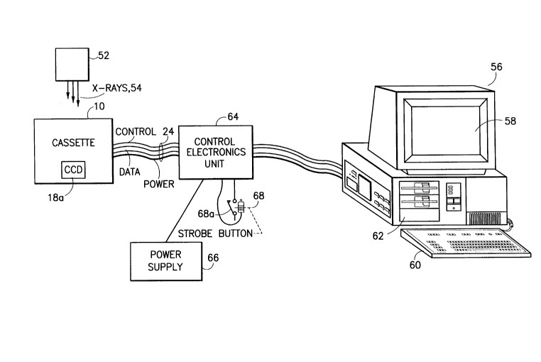
s Fig. 4 is a block diagram of a portion of an x-ray system
50 in accordance with this invention. Although illustrated
in the context of an x-ray system used for a ~ammography
application, including stereotactic needle core biopsy,
preoperative localization, and spot view mammography
applications, it should be realized that the x-ray system
50 using the novel electronic cassette 10 of this invention
is capable of other uses, including industrial inspection,
process control, and a variety of medical x-ray
applications.
A conventional x-ray machine 52 generates an x-ray beam 54
which passes through an object being x-rayed to the
cassette 10. A portion of those x-rays that are not
absorbed within the object are converted to light in the
screen 18c, the light is guided through the bias cut fiber
optic faceplate 18b, and is detected by the CCD sensor chip
18a. The CCD pixel image data is read-out and provided
through the cable 24 to a data processor, such as a PC or
a wor~station 56. The PC 56 includes a high resolution
display 58, a keyboard 60, and an optional high capacity
digital image recorder 62 used for archival and playbac~
purposes. The PC 56 preferably executes suitable image
processing software for displaying the CCD-generated image.
The PC 56 includes a conventional frame grabber (FG) that
is capable of capturing and storing images. Programs for
digitally enhancing the image are provided as required by
the operator or radiologist. Image zooming and other image
manipulation functions are also provided as required.
In accordance with this invention there are provided a
number of features to facilitate the operation, testing,
218819:~
Docket No. LFIS-94-1011 14
and remote configuration of the CCD chip 18a. These
functions are initiated and controlled, in one embodiment,
by a CCD control electronics unit (CEU) 64 that is shown in
Fig. 4. The CEU 64 includes a connection to a power supply
66 and a strobe push-button 68. The CEU 64 routes power
from the power supply 66 into the cassette 10 to power the
CCD chip 18a and the associated electronic ci~cuitry 20.
Alternatively, the functionality of the CCD CEU 64 can be
incorporated into the PC 56, and the cassette power
supplied from the PC 56. These various aspects of the
invention are now described in detail.
In x-ray medical imaging, it would be desirable to be able
to verify from some remote location that the CCD chip 18a
lS and the associated electronics 20 are functioning properly.
For example, it would be desirable to remotely monitor and
detect any possible degradation in the CCD transport
performance and amplifier performance with prolonged usage
in the x-ray environment. The teaching of this invention
provides this capability in the following manner.
In the CCD chip 18a, having the serial readout registers
40a at both the top and the bottom of the array, a test
pattern is electrically injected by a test pattern
generator (TPG) 70 (see Fig. 11) into one of the horizontal
serial registers 4Oa through a VRD node of one of the
amplifiers. The resulting charge packets are clocked into
and through the CCD array and out through another
horizontal serial register 40a. The output charge packets
are then digitized by the associated A/D converter 42 and
output to the CCD tester 64 or PC 56 for evaluation.
A preferred test pattern is typically a burst of e~ual-
sized charge packets in a larger field of zero charge.
Charge trapping within the CCD array is detected if there
is charge missing from the first charge packet, and
2188193
Docket No. LFIS-94-1011 15
transfer inefficiency is detected by the presence of
trailing charge at the end of the burst. This type of test
is readily done in the two-dimensional CCD array by the use
of a checkerboard type of burst pattern.
A further aspect of this invention is the use of an
automatic exposure, also referred to as a pre-~can or low-
dose preview technique. This technique makes use of the
binning capability of the CCD chip 18a, and involves
applying a low dose of x-rays and then summing a
predetermined number of resulting low-level charge packets
from a selected plurality of CCD pixels. A 16x16 summation
or a lOOxlO0 summation are both suitable for use during the
pre-scan. From the magnitude of the charge obtained from
the summation the PC 56 is enabled to determine a maximum
x-ray dose that will be required to obtain an adequate
image. This avoids exposing a patient to a normal dose of
x-rays, determining that the dose was inadequate, and then
exposing the patient to another, possibly larger dose.
The x-ray dosage required for the pre-scan is approximately
l/(X times Y), where X is the number of pixels binned
horizontally and Y is the number of pixels binned
vertically within an area of interest.
Another aspect of this invention is a real-time exposure
control or tracking function. In this mode of operation the
horizontal serial registers 40a are clocked periodically
during the exposure so as to determine an amount of signal
coming into the serial registers. Based on the output
signals the PC 56 predicts when the optimum exposure time
is reached, and the x-ray machine 52 is then signalled to
turn off at that time.
In the presently preferred em~odiment of the CCD chip 18a,
each stage of the serial registers 40a has roughly twice
1 218819~
Docket No. LFIS-94-1011 16
the area of a basic 30x30 micron binned imaging pixel.
Furthermore, the serial registers 40a are also
photosensitive in that they are not covered by metalization
as in many other CCDs. Therefore, by taking an 8X
horizontal summation at the amplifier 40b, there is a 16X
increase in signal level. This allows the PC 56 to sample
the exposure up to sixteen times during the anticipated
exposure period without incurring a loss in signal-to-noise
ratio (SNR). When it is determined that a sufficient amount
of charge has been accumulated during'the exposure, the x-
ray machine is controlled to terminate the exposure.
A further aspect of this invention is referred to as
variable resolution. By example, in medical x-ray imaging
there is a great deal of interest in resolutions
corresponding to pixel sizes ranging from 40 micrometers to
100 micrometers, in addition to interest in other pixel
sizes. Therefore it is beneficial to provide a CCD image
sensor with a wide range of effective pixel sizes to choose
from. For example, with the CCD chip 18a having a basic
pixel size of 15x15 micrometers, the PC 56 programs the CCD
chip 18a to provide one of 15x15, 30x30, 45x45, 60x60,
75x75 microns, etc., output pixel sizes. Preferably the
variation in pixel size is achieved by binning in the CCD
chip 18a, since an improved SNR can be achieved as compared
to digitally combining the pixels afterward. Using this
technique a large variety of pixel sizes (and aspect ratios
or geometries) can be provided on demand. By example, in
addition to the plurality of exemplary square pixel sizes
referred to above, the CCD chip 18a can be cloc~ed to
provide a 4kxl linear "pixel", or a 2kx2 pixel, etc. This
capability also enables the PC 56 to measure a finite
amount of x-ray dose with a very high accuracy.
A further aspect of this invention is automatic x-ray
detection. It can be appreciated that the above-described
'' 21881q3
Docket No. LFIS-94-1011 17
real-time exposure function can be modified to detect the
beginning of the exposure. That is, while waiting for the
exposure to commence, and as will be described in greater
detail below, the vertical clocks are run to continuously
flush out dark current. By also running the horizontal
register clocks and by monitoring the output of the
horizontal shift registers 40a it is possible to detect a
sudden increase in signal level resulting from the onset of
the exposure (typically within approximately 1 millisecond
after the start of the exposure). The vertical clocks can
then be immediately stopped to accumulate charge during the
exposure, without experiencing any significant image
degradation. At this time the horizontal clocks can be
continued for performing the real time exposure control
that was referred to above, and/or to detect the end of the
x-ray exposure.
It should be noted that in a typical mammography
application the entire CCD chip 18a is likely to be covered
by the breast. As a result, there is no direct high-level
x-ray signal available at the CCD chip 18a for use in
detecting the start of the x-ray irradiation period. Also
it is noted that the CCD charge signal for a 30x30
micrometer pixel per millisecond is only approximately 10
to 20 e-, and that at least approximately a 1000 e- signal
is desired in order to make a reliable decision to stop the
vertical clocks for the start of integration.
It is also noted that it is important to the high
performance objective of the system that, prior to the
start of integration, the dark signal be dumped from the
CCD chip 18a at essentially the same rate as that of the
image signal readout.
In order to achieve these goals, a "ready" mode of CCD
clocking includes the steps of: (a) scanning the dark
- 21881 93
Docket No. LFIS-94-1011 18
signal out of the CCD chip 18a at a normal line rate, that
is, at the normal number of pixel rows per second and, in
a time-sharing technique, (b) providing additional clocking
of the horizontal serial register(s) 40a so that x-ray
5 signal can be read separately from the array dark signal.
For example, it is common practice to have some "after-
scan" clock cycles at the end of every line scan. In
accordance with this invention, and for the x-ray detection
function, there are up to approximately 100 after-scan
10 clock cycles per line. By binning the charge resulting
from the after-scan clock cycles at the amplifier 40b, a
large enough signal can be developed to achieve the goal of
obtaining at least about 1000 e- of x-ray signal.
15 By example, if the normal number of horizontal clock cycles
is approximately 4096 array clocks + 10 after-scan clocks
= 4106 total clocks per line, and if these are increased to
4096 + 100 = 4196, the fractional increase is only 2~6.
This increase is insignificant, either in terms of any
20 increased difficulty in providing faster clocks, or in
terms of some small increase in noise level.
As was previously noted, it is preferred to operate the CCD
chip 18a in an uncooled or only slightly cooled mode (such
25 as by using a miniature fan to provide a cooling airflow
over and around the SFOCCD 18). In order to avoid any
unnecessary heating of the CCD chip 18a prior to the
exposure and signal readout, it is desirable to have the
CCD chip 18a and the associated electronics 20 in a low-
30 power standby mode. This minimizes the dark signal andtherefore the noise floor for a given readout time.
Reference is now made to Fig. 9 for showing a presently
preferred method of this invention that accomplishes the
35 low-power standby mode referred to above. At block A the
CCD chip 18a and associated electronics 20 are placed in a
2188193
Docket No. LFIS-94-1011 19
standby or quiescent mode. In this mode all unnecessary
clocks are reduced in frequency or are stopped completely
and, if appropriate, power supply voltages are reduced or
turned off. The system remains in this state until
activity is detected at block B. The detection of activity
can be accomplished by providing the operator with a push
button switch to indicate that an exposure will soon be
taken. It is also within the scope of the invention to
mount the hand-held strobe button 68 shown in Fig. 4, which
is used by the operator to initiate an exposure, to a
switched mounting 68a. In this manner, when the operator
removes the hand-held strobe button 68 from the mounting
68a a switch is activated. The change in state of the
switch is detected by the CCD CEU 64 (or PC 56) and is
interpreted as a change in state of system activity (i.e.,
that an exposure will soon be made). It is also within the
scope of this invention, and referring also to Fig. 3, to
employ a proximity or other type of sensor to detect that
the breast has been compressed prior to making an exposure.
Assuming now that a determination has been made at block B
that activity has started, the method transitions to block
C where the CCD chip 18a is armed and the dark current is
flushed from the pixels. In other words, the CCD chip 18a
2s and associated electronics 20 are brought out of the
quiescent mode to a full operational status, and the
vertical clocks are run so as to remove the dark current.
A complete flush of the dark current may take, by example,
three seconds. At block D a determination is made if the
x-ray exposure has started. This can be accomplished, as
was described above, by oversampling the horizontal
registers during the dark current flush and then binning
the oversample readouts to determine an increase in charge
that is generated by the horizontal registers 40a in
3s response to the x-ray flux. The system loops through blocks
C and D to continuously flush dark current and wait for the
2188193
. . ~
Docket No. LFIS-94-1011 20
start of the exposure.
Assuming that the start of the exposure is detected, at
block E the vertical clocks of the CCD chip 18a are
i_mediately stopped so as to initiate the integration of
charge within the individual pixels. The horizontal
register clocks can continue to run so as to (1~ detect an
onset and a termination of the exposure, (2) to perform the
automatic exposure length function that was referred to
above, and/or to (3) perform the real time exposure control
function. If this latter function is performed then it may
not be necessary to also perform the detection of the
termination of the exposure. If desired, the prescan
function referred to above can also be performed. The
system loops between blocks E and F until the exposure is
terminated, at which time control passes to block G to
readout the integrated charge that resulted from the
exposure. Control then passes to block A to re-enter the
low power quiescent mode until activity is once again
sensed.
A further aspect of this invention is an ability to
remotely perform an automatic optimization of image
quality. Referring to Figs. 10 and 11, this function is
accomplished by having clock duty cycles and levels, and
also dc-bias potentials, set by digital-to-analog
converters (DACs) and other circuitry. As a result, the
capability is provided to remotely control bias and clock
potentials and waveshapes, and to then P~m; ne the
resulting output of the CCD chip 18a, such as was described
previously with regard to the remote testability function.
Based on the output of the CCD chip 18a for a given
combination of clock and bias potentials, the PC 56 is
enabled to determine optimal settings for such parameters
as: (a) lowest dark signal (optimum MPP (multi-pinned
phase)), (b) best vertical transfer efficiency, (c) best
2188193
Docket No. LFIS-94-1011 21
horizontal transfer efficiency, etc. In this regard it
should be realized that the PC 56 need not be in the same
location as the x-ray machine 52. In fact, the PC 56 could
be located a considerable distance away, such that the data
5 links between the PC 56 and the cassette 10 are conveyed,
by example, telephonically though a modem connection.
Referring first to Fig. 10 there is shown a portion of the
support electronics 20 in accordance with this aspect of
10 the invention. A shift register 72 is provided for
receiving a data signal (D) from the PC 56, via a local
controller 78 as shown in Fig. 11. In this embodiment of
the invention a total of 32 bias signals are generated,
each having, by example, 12 bits of resolution. At the
15 outputs of the shift register 72 a plurality (e.g., 32)
DACs (DACsl-i) 74 are connected for receiving 12-bit
inputs. The analog outputs of the 32 DACs 74 provide the
32 bias potentials. Some of these bias potentials are used
for setting the high and low excursions of the required
20 clock signals (10 clocks total requiring 20 clock bias
potentials). One of these clock circuits is shown as an
amplifier 76 that receives a processed clock (PCLK) signal
from a delay width controller 82 shown in Fig. 11. Two
bias potentials (e.g., BIASl and BIAS2) are connected to
25 the high and low power rails of the amplifier 76. By
controllably adjusting the magnitudes of BIASl and BIAS2
the cloc~c excursions can be correspondingly controlled.
Other bias potentials are provided to the CCD chip 18a and
the amplifiers 40b as required. By example, the VDD input
30 to the amplifier 40b in Fig. 5 is connected to a diode
within the CCD chip 18a. By controlling the conduction of
this diode via the magnitude of VDD the image readout is
also controlled.
35 In Fig. 11 the local controller 78 is shown connected to
the bus 24. The local controller 78 outputs the data signal
21881~3
Doc~et No. LFIS-94-1011 22
(D) to the DACs 74 via the shift register 72, and also to
a delay shift register 80. The output of the delay shift
register 80 is provided to the above mentioned delay width
controller 82 for specifying the pulse widths or duty
cycles of the processed clock signals (PCLKs). The delay
width controller receives "raw" clock signals (e.g., 50
MHz) from a clock source that is generated either within
the cassette 10 or externally and received through the
cable 24.
In operation, and by example, the PC 56 can optimize the
dark current by adjusting the bias potentials until a
desired dark current level is reached. In this regard the
PC 56 obtains an optimum MPP mode by controllably
lS decreasing the various clock signal low rails while
continuously monitoring the dark current so as to set the
dark current at a minimum value. It can be appreciated that
this tas~ would be tedious and time consuming if done
manually, and furthermore would require the attention of a
skilled technician or engineer.
After the optimum bias values are determined by the PC 56,
these values can be stored and later recalled and
downloaded via the cable 24 to the optimization circuitry
shown in Figs. 10 and 11. As was previously noted, the PC
56 can be remotely located from the x-ray system and
cassette 10. Alternatively, the data representing the
optimum operating parameters for the CCD system can be
stored within a non-volatile memory within the cassette 1,
and then subsequently recalled by the local controller 78
for setting the DACs 74 and/or delay width controller 82
accordingly.
Based on the foregoing it should be noted that this
invention provides a closed loop capability to remotely
test, diagnose and/or calibrate a CCD-based x-ray image
' 21881~3
Docket No. LFIS-94-1011 23
sensor, wherein an external controller is enabled to
controllably stimulate the CCD-system, read-out the
resulting signals, and then vary the stimulation to obtain
a desired output. For example, clock biases and delays can
be individually adjusted, a test pattern introduced via the
TPG 70, and the resulting output analyzed to determine a
correct setting for the large number of variables (clock
duty cycles, clock biases, CCD-biases, etc.) which must be
considered in order to optimize the image-gathering
capability of the SFOCCD 18.
The Appendix sets forth a number of exemplary CCD and
support electronics operating parameters and their typical
ranges. It is within the scope of this invention to provide
for remote programmability of one or more of these
operating parameters. It should be noted that the various
potentials can in practice be driven through a range of, by
example, +25 V, with clock rates up to, by example, 50 MHz.
In this manner it is possible to compensate for process
variations between CCDs. Furthermore, and for a multiple
CCD embodiment, the teaching of this invention enables each
of the CCDs to be separately adjusted and optimized.
By example, offset compensation can also be accomplished to
accommodate the change in the level of the output DC of the
video signal as a function of CCD device, temperature and
time. One preferred method for performing offset
compensation is as follows. First, the ADC clocks are
changed to sample the reset level on both legs of the ADC.
Next, the front end offset (FEO) is changed to minimize the
offset reading from the ADC. The ADC clocks are then
changed to sample the reset and the reference shelf
potentials. These readings are then minimized by again
varying the front end offset. Finally, the ADC clocks are
restored to a normal operating mode. In accordance with an
aspect of this invention, all of these functions can be
2~88193
.
Docket No. LFIS-94-1011 24
performed remotely by programming the various CCD support
electronics and circuitry.
Thus, while the invention has been particularly shown and
described with respect to presently preferred embodiments
thereof, it will be understood by those skilled in the art
that changes in form and details may be made therein
without departing from the scope and spirit of the
invention. By example, the various dimensions, lay-out,
clocks and clock frequencies referred to above are
exemplary of but one suitable CCD device for practicing
this invention, and are not to be considered as a
limitation on the practice of this invention.
As such, the scope of the teaching of this invention is not
intended to be limited to only the embodiments that have
been expressly disclosed and illustrated, but instead the
teaching of this invention should be read as being
commensurate with the scope of the claims that follow.
APPEND~X ~ 2~ 8-8 1 9 3
~, p. A--1
DC VOLTAGES RANGES
sY~soL C~IARACTERISlIC RANGE UNITS
MlN TYP ~X
VDD Output Arnplifier Drain Supply Voltage 15.0 22.0 25.0 V
VRD Output Reset Drain Supply Volhges lO.O 12.0 :20.0 V
VOG Output DC Gate Voltages O.O 0.5 5.0 V
VRT Amplifier Signal Ground O.O 3.0 5.0 V
VSS Subslrate Bias ~-~ V
CLOCK BIASES RANGES
SYMBOL CHARA~ 1 lC RANGE IJNII S
M~ m MAX
V0H HIGH Horizontal T~ ull Gate HIGH 2.0 5.0 8.0 V
V0SG HIGH Output S~ ;.-p Gate HIGH 2.0 5.0 8.0 V
V0R HIGH Reset Gate HIGH 5.0 8.0 15.0 V
V0V HIGH Ver~ical T al~5~)0ll Gate HIGH O.O 3.0 -!5.0 V
V0VTG HIGH Ver~ical Transfer Gate HIGH O.O 3.0 5.0 V
V0H LOW Horizontal Tla~ s~oll Gate LOW -8.0 -5.0 -2.0 V
V0SG LOW Output S~ .. n.n~ Gate LOW -8.0 -5.0 -2.0 V
V0R LOW Reset Gate LOW -5.0 O.O 5.0 V
V0V LOW Vertical T.d~poll Gate LOW -lO.O -8.0 -5.0 V
V0VTG LC)W Ver~ical Transfer Gate LOW -lO.O -8.0 S.O V
ELECTRONICS SYSTEM CONTROLS
S~fBOL C$~RAcTER~STIc RANGE UNlTS
MIN TYP MAX
FEG Front End Gain 1:1 25 :1
FEO Front End Offset O 14 V
BEG Back End Gain 1:1 25:1
BEO Back End Offset O 5 V
ADC DLY ADC Clock Delay O 512 n.s.
RST_DLY Reset Shelf Sample Delay O 512 n.s.
PXL_DLY Pixel Sample Pulse Delay O 512 n.s.
0~ SMP ADC Pixel Oversarnpling 1 4 tirnes