Note: Descriptions are shown in the official language in which they were submitted.
WO 96/26910
~ 1 882~
NOVEL SILICON CARBIDE WMMY WAFER
BACKGROllND OF THE INVENTION
The manufacture of semi ~---~-l - ~nr device6 such as diodes
and transistors typically requires nYi(li7;ng the surfaces of
5 thin silicon wafers, etching cavities in the surfaces of those
wafers, and depositing a dopant ti.e., boron, pho~ullo~ous,
arsenic, or antimony) in those cavities, thus forming
transistor contact points. The oxidation and doping operations
involve rapid heat and cool cycles in an electrically heated
furnace at t~ GtUL~s ranging from 1000C to 1350C. After
the surface has been etched, the dopant is usually fed as a gas
into the necked down end of a diffusion process tube placed in
the furnace. The gas then diffuses into the etched cavities
and deposits on its surfaces.
During the oxidation and diffusion steps, the silicon
wafers sit on boats or plates placed within the process tube.
The wafer boat and process tube are typically made of a
material which has excellent thermal 6hock resistance, high
-`-nicAl ~,L~.U,Ll., an ability to retain its shape through a
20 large number of heating and cooling cycles, and which does not
out-gas (i.e., i.,Llu-luce any undesirable impurities into the
G; ~' -re of the kiln during firing operations). One material
which meets these requirements is siliconi7ed silicon carbide.
When the silicon wafers are processed in a boat, it is
25 naturally desirable that each wafer in the boat be exposed to
identical gas conc~..L~Gtion and temperature profiles in order
to produce consistent product. However, the typical
llyd~udyl,amic situation is such that consistent profiles are
found only in the middle of the boat while inconsistent
30 profiles are often found at the ends of the boats, resulting in
undesirable degrees of dopant deposition upon the end-wafers
which render them unusable.
One conventional method of mitigating this "end-effect"
problem is to f ill the end slots of the boat with sacrif icial
35 silicon wafers. However, it has been found that silicon wafers
are expensive, extensively out-gas, warp at high process
temperatures, flake particles, and have a short useful life
span .
SUBSTlTUrE SHEET (RULE 26)
WO 96126910
~ 21 88~90
Another conventional method of mitigating the "end-effect~
problem is to fill the end 610ts of the boat with "dummy"
wafers. For example, one investigator placed SiC-coated carbon
wafers having the exact dimensions of the neighboring silicon
5 wafers in the end slots. However, these wafers were found to
break apart, contaminating the furnace with the exposed carbon.
Another investigator ~ osed using CVD monolithic silicon
carbide as a dummy wafer. However, this material is known to
be very expensive.
lC Japanese Patent Publication 5-283306 discloses a
;cnn;70~1 silicon carbide dummy wafer having an
alumina/silica coating.
Therefore, it is the object of the present invention to
provide an inexpensive dummy wafer which posCDccDc the
tl;- ionql ~ physical and qn;cql properties required for
dummy wafers .
6UMMARY OF THE INVEN~ION
In accordance with the present invention, there is
provided an lln~il;r~n;7ed wafer consisting essentially of
L~_ly~l ,.11; 70'1 silicon carbide, the wafer having a diameter of
~t least 150 mm and a thickness of no more than 2 mm, and
having a porosity of between 15 v/o and 43 v/o.
Also in accordance with the present invention, there i8
provided a recrystallized silicon carbide wafer having a
diameter of at least 150 mm and a th i rl-nP~c of no more than 2
mm, and comprising between 15 v/o and 43 v/o free silicon, and
a CVD silicon carbide coating thereon.
Also in accordance with the present invention, there
is provided a recrystallized silicon carbide wafer having
a diameter of at least 150 mm and a thickness of no more
than 2 mm, and comprising between 25 and 40 v/o free
silicon, the free silicon comprising coarse interconnected
free silicon pockets having 5 to 50 micron diameters.
DESCRIP~ION OF ~HE FIGURES
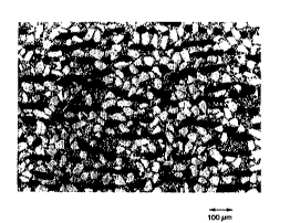
Figure 1 is a photomicrograph of conventional
unsiliconized silicon carbide, wherein the light regions
represent silicon carbide and the dark regions, eplesellL
porosity .
SUBSTITUTE S~IEET tRULE 2~i)
~-
~ WO96/26910 2 ~ ~82~a PCT/US96/02880
Figure 2 is a photomicrograph of an unsiliconized
--nt of the pre6ent invention, wherein the light regions
represent silicon carbide and the dark regions represent
porosity .
n~ TT T n DES~:Kl~LlON OF THE INVENTION
For the ~u.~oses of the present invention, "v/o" refers to
a volume percent, "w/o" refers to a weight percent and a
"conventionally ~Luduced" product refers to si-sic products
made in accordance with US Patent No. 3,951,587 ("the Alliegro
patent"). In addition, the term "flatness" is considered to be
the maximum bow height from a mean datum line, the mean datum
line being defined by an arbitrary diameter at the surface of
the waf er .
The initial efforts of the present inventors ~YAm; nF~r~
cilir~lni7ec~ silicon carbide, specifically CRYSTAR~ (containing
about 15% free silicon and about 85% bimodal sic, manufactured
by the Norton Company of Worcester , MA), as the dummy waf er
material. However, it was found that the conventional CRYSTAR~
casting process (a bimodal SiC blend slip-cast in a porous
pla6ter mold~ could not s~lccPcsfully produce a thick billet
.hl~- to slicing. In particular, when the 61ip was slip-
cast thicker than about 20 mm in depth, the resulting billet
would develop cracks upon drying or f iring due to residual
stresses .
It is believed this process failed because water retained
in the green body pores after slip-casting turned into
e~LL~y~ed steam upon subsequent heating. The internal ~lL~::sr~uL~
buildup generated by the steam forced the cast body to crack
and warp. The present inventors noted the conventional slip
cast approach ~Loduced only about 15 v/o porosity and pore
rhAnnPl c of only about 2 microns (as measured by mercury
porosimetry) in the cast body and hypothesized that this level
of porosity was not substantial enough to provide continuous
rhAnn~.l c suitable for the escape of retained water during
3s conventional drying. They also contemplated that the density
gradients pL~.duced by conventional slip casting contributed to
the cracking problem, as these gradients produced thermal
stresses on heating.
SUBSTITUTE SHEET ~ULE 26)
W0 96/26910 - ~ 2 1 8 8 2 9 0
The present inventors al60 ~YAllli n~l open-face casting. The
open face casting approach produced a thin wafer having a
thickness of about 3 mm (to provide for warpage during firing)
which wa6 then 6urface ground to the de6ired 0.5 - 1.0 mm
5 thickness. The fired product had a poro6ity of about 15-16 ~
v/o. ~owever, because the required grinding operation is labor
inten6ive and removes over half of the wafer stock, open face
- ca6ting was con6idered to be prohibitively inefficient and
expensive. Further attempts to open face cast the slip closer
l~ to the desired wafer thickness resuited in green wafer6 that
warped during drying and f iring .
The pre6ent inventor6 then con6idered freeze-casting a
bimodal silicon carbide slip and l~n~Yrer~-lly found that freeze
casting provided a thick, dimensionally correct billet which
15 did not warp or crack during pror~csin~ was ea6ily sliced, and
maintained sufficient ~-L~IlyLll a~ter it was sliced.
It i6 believed that the freeze casting proce6s yields a
green body billet which is particularly suited to the
requirement6 of large 6cale production of sic dummy wafer6.
20 when a 61ip is freeze cast, the water undergoes a 4~6 volume
expansion as it becomes ice crystals. Since freeze casting is
performed in a closed volume, the ice particle expansion has
the effect of packing the sic particles closer together (when
compared to slip cast sic packing) in the regions not taken up
2s by the ice particles. Moreover, it has been observed that the
ice crystais formed in freeze casting are interconn~ct~
thereby forming pore r~ nnrll c upon drying. Therefore, although
the freeze cast body pOc$F~:5~c the same overall volume percent
solids as the conventional slip ca6t body (i.e., about 72 vjo),
30 the freeze cast body has both largér, interr~nn~rt~d pores and
better interparticle bonding. The better interparticle bonding
provides not only good strength for the cast body (despite the
larger pore size) but also good strength for the sintered body,
~s the more highly packed sic grains more readily form necks
3s during recrystallization. Because the interconnected pore6
provide a channel for steam escape and the superior particle
bonding provides superior strength, it appears that freeze
casting avoids the problems encountered in the conventional
SUBSTITUTE SHEET (RULE 2~)
~ WO 961269l0 2 1 8 8 2 q ~
slip casting process for large scale SiC dummy wafer
production .
Another advantage of the present invention is that its
- preferred process need not include the vacuum sublimation step
s typically required during conventional silicon carbide freeze
casting. Without wishing to be tied to a theory, it is
believed that vacuum sublimation is not required because
compaction of the SiC grains during freezing yields a
relatively rigid skeletal structure resistant to vc L (and
lo therefore cracking) when the water is removed. In addition,
the relatively large pore rh;~nn~l c formed by the ice crystals
provide reduced capillary ~cs_u,cs and reduced drying
L r csses .
In one pref erred ' ' i L of the present invention, a
SiC-based wafer is made and used in a process comprising:
a) mixing silicon carbide powder, water, and an ice-
crystal growth inhibitor to produce a slip,
b) freezing the slip at about -85C to produce a
frozen casting,
c) air drying the frozen casting to partially remove
the water,
d) drying the casting at about 200C for about 24
hours,
e) vacuum presintering the body to produce a
2s recrys~ l l i 79C~ billet having a green strength of
about 3 5 IqPa,
f) slicing the billet into wafers,
g) optionally, siliconizing and/or CVD coating the wafers,
~nd
h) placing the wafers in a boat.
In the above-described ~mho~ir t, the slip typically
comprises a bimodal sic powder distribution comprising between
about 15 and about 41 v/o coarse sic grains having a particle
size ranging from 10 to 150 microns ("the coarse fraction"),
3s and between about 34 and about 60 v/o fine SiC grains having a
particle size ranging between 1 and 4 microns ( "the f ine
fraction"). Preferably, the fine fraction comprise~ between
about 36 and 42 v/o of the slip and has an average particle
size of about 2-3 microns, while the coarse fraction comprises
SUBSTTTUTE SHEET (RULE 26)
W0 96126910 2 1 8 8 2 0 . r ~
between 33 v/o and 38 v/o of the slip and has an average
particle size of about 60 microns. ~ When the coarse SiC
particle size is above about 150 microns, it approaches haif
the u L-.Ss s~_-ion of the final wafer and grain pullout during
slicing is observed in the f inished waf er .
Water ls generally included in the slip in an amount
sufficient to produce a slip having from about 50 to 85 v/o
solids. However, othQr solvents amenable to freeze ca6ting
(such as glycerol, ethanol, methanol, hexane) may be suitably
lo used as the slip's liquid carrier.
The slip also preferably contains an icQ-crystal growth
inhibitor. Typical freeze casting techniques create ice
crystals as large as 5000-10000 um on both the inside and
outside of the frozen casting. Subsequent fteeze drying and
firing of these bodies reveal large isolated pores (the
remnants of the large ice crystals). These isolated pores act
as flaws which degrade both green and final 6trength. The ice-
crystal growth inhibitor pL~V~ Ll, large crystal formation by
forcing the 51ip to freeze in the form of minute crystals on
the order of only 5-50 microns. Typical ice crystal growth
inhibitors include ~l~dLU~el~ bond-forming a_ such as
glycerol and 2~11 of the ~ ~ similarly identif ied in U. 5 .
Patent No. 4,341,725 ("the Weaver patent"), the entire
rreC~ ~ication of which is incu.~uL~ted by reference.
Typically, the ice crystal growth inhibitor comprises between
about 0.2 w/o and about 5 w/o of the slip, preferably between
about 1 w/o and about 1.5 w/o. In more preferred . ~--~i Ls,
glycerol comprises about 1 w/o of the slip. The required
amount of ice crystal growth inhibitor also depends on the
solids content of the slurry, with high solids content slurries
requiring less inhibitor. Other typical components of the slip
include conventional amounts of conventional casting additives.
For example, deflocculating agents such as NaOH and Na25iO3
may be used. A binder may also be present in the range from
about 0.25 w/o to 4.0 w/o solids. In preferred ~ ; -ntS, an
acrylic latex binder is used at a level of about 1 w/o of the
solids .
In order to insure a homogeneous sIip, the slip
components are typically mixed in a ball mill evacuated to a
SUE~STITUTE SHEET ~RULE 26)
~ wo 96n69l0 2 1 8 8 ~9 ~ r~
vacuum level of between about 27 and 30 inches Hg and rolled
f or at least about 17 hours .
The freezing step of this Pmho~ (often callecl,
"freeze casting") preferably includes pouring the slip into an
S ; --hlP mold and lowering its t-, ~tUL~: until the liquid
carrier freezes, thereby solidifying the slip. Freezing the
slip generally entails lowering its temperature to between
about -20C and -100C for between about 30-180 minutes,
resulting in a freeze-cast body having only small (i.e., 5-50
lo micron) ice crystals. Preferably, the; --hlP mold is made
of silicone rubber which can be easily peeled from the frozen
body .
The air drying step of the pref erred pmhQ~9; r t serves to
remove enough free water from the casting to allow it to be
1S placed in a heated oven without cracking. Air drying can be
effectuated by simply removing the frozen body from its mold
and letting it stand in air for about 24 hours. Typical
conditions and drying times for air drying range between 20 and
30C, preferably 25C; between about 0.01 and several atm
20 pLesDuL?~ preferably 1 atm EJLe:SDULe; and between about 18 and
about 48 hours, preferably about 24 hours.
The high temperature drying step of the above ` ;- L
is typically performed at a higher temperature and for a longer
duration than the air drying step and removes essentially all
25 the absorbed water in the casting. Typical conditions and
drying times for this step range from between 80C and 200C,
preferably 140C; between about 0.01 and 1 atm ~ SDULC,
preferably 1 atm ~L~:8~UL-'; and between about 18 and about 48
hours, preferably about 24 hours. It was l~npyrprtp~lly found
30 that the freeze cast body can be suitably dried at ~ -ric
eDDuLe under these conditions without cracking. As noted
above, conventionally processed, slip cast sic bodies were
f ound to crack under high temperature, atmospheric drying
conditions. Because the freeze drying process does not require
3s subsequent vacuum drying, it is significantly less expensive
than conventional sic processing.
The dried casting produced in accordance with this
: ` :';- t exhibits a bulk density of at least about 1.8 g/cc
and a four point bending strength of at least about 5 MPa. Its
SUBSTITVTE SHEET (RULE 26)
wo 96n69l0 ~ PCrlU596/02880
,
21 88290
pore ~ize ranges from aoout 5 to 50 micronF . Its average pore
size is about 15 microns. In contr2st, the conventional dried
SiC casting has an average pore size of only about 2 microns.
The vacuum presintering step of the preferred Pn~ho~
s serves to establish recrystallization ( i . e., neck growth
between the SiC grains without densif ication) without cracking .
It may be carried out at about 1900-1950C under a vacuum of
about 0 . 5 torr in an Ar atmosphere . Whereas conventional SiC
castings were found to crack under these conditions, it is
lo believed the freeze cast bodies of the present invention did
not crack because the relatively large pore e hAnn~l c formed by
the ice crystals result in low capillary pressures and low
"LL-~aes on drying, as well as a uniform density across the
part which resists thermal stresses.
The recrystallized billet produced in accordance with this
L exhibits a bulk density of at least about 1. 8 g/cc.
Its porosity ranges from 25 v/o to 43 v/o. Its pore size
ranges from about 5 to 50 microns. Its average pore size is
about 15 microns. In contrast, the conventional recrystallized
20 SiC casting has a porosity of about 16 v/o and an average pore
~ize of about 2 microns. Its strength (as measured by ring on
ring biaxial flexure) is at least 30 NPa, typically between 30
and 5 0 MPa .
After presintering, the recrystAlli7~d billet is sliced by
2s conventional processes ( i . e ., a diamond wheel or wire) to its
f inal tl i ~ n In contrast to less porous conventional SiC
billets, the recrystAlli7~l SiC billet of this embodiment is
easily sliced into thin SiC wafers. The structure of the
presintered billet is such that it has sufficient handling
30 strength, but is quickly and easily sliced to a good surface
finish and flatness. For example, a 1 mm thick wafer produced
in accordance with the present invention may be sliced from a
15 cm diameter billet in only about 5 minutes. In contrast, it
is believed that a higher density slip cast SiC billet would
35 require about 60 minutes and a fully dense sic bil1et would
require about 120 minutes to slice. Recrystallized silicon
carbide dummy wafers having diameters of between about 150 and
about 300 mm, thi~knt~cc~c between about 0.5 and about 2 mm,
preferably between 0.5 mm and 1.5 mm, more preferably between
SUBSTITUTE SHEE~ tRULE 26)
- .
wo s6n6sl0 r~
2 1 882~0
about 0.5 and 1.0 mm; and fl~ .ess~s of between about 25 and
about 100 microns, preferably les6 than about 50 microns, are
obtainable in accordance with this ~mhorl;~ n t, usually after
mere diamond saw slicing. If the wafer is subsequently
S siliconized, it may need to be rotary ground for a short period
to remove a few microns and attain a flatness of less than 100
um.
The final firing step makes the wafer illl~r -hl~ to gases
or liquids. It typically involves either impregnating the
porous wafer with silicon to eliminate porosity and/or CVD
coating it with an; ~~hle ceramic such as silicon carbide.
If s;licon;7ing is select~d, it may be carried out in
accordance with US Patent No. 3,951,587 ("the Alliegro
patent" ), the specif ication of which is incorporated by
reference. It was ~n~Yr~ct~ly observed that the siliconized
wafers had a flatness of about 100 um. In contrast,
dimensionally similar conventional "green" sic castings have
been found to excessively warp, necessitating a thicker casting
and expensive final r--h;nin7 in order to produce the same flat
product.
The ~ilic~ln;~ecl wafer of a preferred: '_'tr ~ oE the
present invention exhibits a bulk density of at least about
2 . 75 g/cc. Its pockets of free silicon range from about 5 to
50 microns in .1;, t.l:L. It is fully dense. In contrast, a
2s conventionally ~L~,.Iu. ed siliconized SiC wafer has pockets of
free silicon that are only about 2 microns in diameter.
The microstructure of this ~mho~ of the present
invention appears to have three distinct phases of the
material, comprising: a coarse grain SiC phase, a coarse free
silicon phase; and a mixed phase comprising fine SiC grains and
fine free silicon pockets. D~r~n~lin~ upon whether the SiC
dummy wafer is siliconized, the sic wafer typically comprises:
a) between about 15 v/o and 41 v/o (preferably 33 to 38
v/o) silicon carbide grains having a diameter of between
10 um and 150 um,
b) between about 34 v/o and 60 v/o ~preferably 36 to 42
v/o) silicon carbide grains having a diameter of between l
um and 4 um, and
c) between 25 v/o and 40 v/o free silicon or porosity.
SUBSTITUTE SHEE~ (RULE 26)
W0 96126910 , ~ 2 ~ 8 8 2 9 0 PCTIUS96102880
The porosity o~ the l~nci 1 l rnn; 7e~ wafer is characterized by a
bimodal size distribution of coarse (5-50 um) pore5 and fine
pores, while the free silicon of the slliconized wafer is
characterized by free silicon pockets having 5-50 micron
S diameters and a free silicon matrix which ~uLLuul-ds fine SiC
grains. See Figure 2. In some `~_~i r ~s, there is preferably
between 35 v/o and 40 v/o free silicon. In comparison, prior
~rt microstructures were found to be characterized by a uniform
structure of a mixed phase compri6ing large grain SiC, small
lo grain sic and small free silicon pockets or porosity. See
Figure 1.
Sandblasting of the siliconized sic wafer can remove
excess free silicon that has exuded to the surface due to the
volu~e expanslon of silicon on solidification, and r~ay be done
15 by conventional sandblasting processe~: . Because these waf ers
possess high strength, they do not break when subjected to
~;~n~hl ~cting.
Although the above-d~crr;hed ~ ;r- ~ of the~ present
invention exploits freeze casting to produce a thin, strong sic
20 wafer, it is also anticipated that useful sic wafers can be
obtained by a number of alternative ~LuueSses~ including: ~)
warm pressing a sic billet at 1750C and 3000 psi; b) gel
casting and presintering a SiC billet in ~crnr~s~nre with U. 5 .
Patent No. 5,145,908; c) cold isostatic pressing a sic billet,
25 and d) tape casting or roll pressing and then recrystallizing a
SiC slip to produce a fired sic wafer having a porosity of
about 21%.
The novel recrystallized silicon carbide ceramics of the
present invention may be used in conventional 5~1 jrnn;7ed
30 silicon carbide or CVD coated silicon carbide applications,
;nr~ ;ng those applications disclosed in the Alliegro patent.
Tt may also find application as a rigid disc in computer hard
drives, as a substrate for other electronic applications, or as
baffle plates in wafer boats. In particular, therè is
35 contemplated a silicon carbide disk substrate for use in a disk
drive assembly having a head and a disk, the disk comprising
the disk substrate, wherein the disk substrate comprises a)
between 15 v/o and 43 v/o free silicon or porosity, preferably
between 25 v/o and 40 v/o; b) preferably having a flatness of
1~ ~
SUBSTITUTE SHEET ~RULE 261
WO 96126910 2 18 8 2 9 0 r~~
between i5 um and l00 um; c) preferably having a bimodal SiC
grain distribution of coarse and fine grains; and d) preferably
having a bimodal free silicon or pore distribution of coarse
and f ine pores . Other contemplated uses of the highly porous
s silicon carbide discs of the present invention (which could
exploit the low pressure drop across the disc) include gas
burner plates, composite substrates and filters.
In some ~hoAi- ~s, the porous wafer of the present
invention is optionally coated with a layer of either
polysilicon, silicon nitride or silicon dioxide, placed in a
diffusion boat in which silicon wafers are also s1~hcr-qur-ntly,
and the silicon wafers are processed at a tr, ~LUL~ of at
least about 600 degrees C.
In some: ` 'i Ls, the cil icrni7r-(~, Sic CVD coated wafer
lS of the present invention is placed in a diffusion boat in which
silicon wafers are subsequently placed, and the wafers are
pL~ce4~ed at t~ lltUL ~s above l000 degrees C. It is believed
the CVD SiC coating is necessary at those temperatures to
prevent oxidation of the SiC grains. Therefore, there is also
provided a process comprising:
a) placing a silicon wafer in a diffusion boat having the
siliconized, SiC CVD coated wafer of the present invention
placed therein, and
b) processing the silicon wafer at a t~ ~tUL~: above
2s about l000 degrees C.
Also in accordance with the present invention, there is
provided a method of single wafer processing, comprising the
steps of:
a) providing a silicon carbide wafer of the present
invention (preferably having a diameter of at least 200 mm
and more preferably at least 300 mm) in a substantially
horizontal position, and
b) placing a silicon wafer (preferably having a diameter of
at least 200 mm and more preferably at least 300 mm) upon
3s the silicon carbide disc, and
c) heating the silicon wafer at a rate of at least l00 C per
second .
Also in ac-_vldc,nce with the present invention, there is
provided a method of cleaning single wafer processing chambers,
11
SUBSTITUTE S~IEET(RULE 26)
wo s6n6sl0 r~
- ` 21 882~0 ` ~
comprising the steps of:
a) providing a susceptor in a processing chamber,
b) placing a silicon wafer upon the susceptor,
c) proc¢ssing the silicon wafer,
S d) removing the silicon wafer,
e) placing a silicon carbide wafer of the present invention
(preferably having a diameter of at least 200 mm and more
preferably at least 300 mm) over the susceptor, and
f ) cleaning the processing chamber.
Also in a.ouLd~ e with the present invention, there is
provided a method of flat panel display processing, comprising
the steps of:
a) providlng a silicon carbide wafers method of the present
invention (preferably having a length of at least 165 mm and
lS a width of at least 265 mm) in a substantially horizontal
positlon, and
b) placing a flat glass plate (preferably having and length
and width of at least 100 mm) upon the silicon carbide disc,
and
c) processing the f lat glass plate.
A160 in a~;curdal~.c with the present invention, there i6
provided a method of plasma etching silicon wafers, comprising
the steps of:
a) providing a silicon wafer having a pr~ t~rm;n~rl diameter
of at least 200 mm,
b) placing a silicon carbide ring of the present invention
(having an inner diameter essentially equal to the
prPrl~t~m;nPd diameter of the silicon wafer) around the
silicon wafer, and
b) plasma etching ~preferably dry metal plasma etching) the
~ilicon wafer.
EXAMPLE I
~ freeze cast slurry was prepared by mixing the following
materials in the quantities shown in Table I, and rolling in a
3s ~ar for 18 hours.
- TAr3LE I -
Silicon Carbide (3 micrûn) 4680g
Silicon Carbide (lOOF) 4320g
Water 1080g
12
SUBSTITUTE Sl iEET ~RULE 26)
~ WO 96/26910 2 1 8 8 2~ 0 PC~IIUS96/02880
BASF Acranol 290D Binder 137g
NaOH (lN) 81g
Baker Glycerol 90g
The slurry was vacuum deaired and poured into a polyvinyl
, chloride tube having an inner diameter of 6", an outer diameter
of 6.5" and a height of 10". The tube was clamped to a glass
5 plate to prevent leakage and form the bottom surface. The
assembly was then placed in a freezer at -85C for 3 hours.
After being fully frozen, the tube was cut away from the
billet. The freeze cast billet was initially air dried at
about 25 C for 18 hours and final dried at 140C for 48 hours
10 to remove the absorbed water. The billet was then sintered at
about 1900C in an argon atmosphere to effect
~ Ly~-L~llization. The porous LC~LY`l~I11 i 7~d billet was dry
sliced with a metal bonded diamond saw to a thickness of
0.040". The wafer was infiltrated with molten silicon at about
15 1800C in an argon/nitrogen a, , ^re and then sandblasted
with sic grain to remove any excess silicon. The s~n~lhlAqted
wafer had a flatness of about 100 microns. Rotary grinding
with a diamond abrasive provided a flatness of about 50
microns. It is contemplated that final lapping with a boron0 carbide slurry could produce flatness of 20 microns.
EXAMPL~ II
A l-n;- 1 silicon carbide slip having an average size of 3
microns was hot pressed in a graphite die at about 1850C and
3000 psi for 1 hour. The billet had a 3" diameter, a 4"
2s height, and a density of about 2 . 0 g/cc (about 62% of
theoretical density). The billet was dry sliced with a metal
bonded diamond wheel to a thickness of 0.75 mm. The wafer was
infiltrated with molten silicon at about 1800C in an
argon/nitrogen ai ~ . The siliconized wafer was then
30 sandblasted with SiC grain to remove any excess silicon. The
sil;ron;~ed wafer had a flatness of about 70 microns. Some of
the ~nahl~cted wafers were coated with about 50 microns of SiC
by rh~-~;r~l vapor deposition of methyltrichlorosilane in
ll~dLoy~ and argon at about 1100C.
13
SUBSTlllJTE SHEEl- ~RULE 263