Note: Descriptions are shown in the official language in which they were submitted.
21 89322
Se 30.10.95 95/133
TITLE OF THE lNV~NllON
Electrical switching device
BACKGROUND OF THE INVENTION
Field of the Invention
The invention is based on an electrical
switching device according to the preamble of claim 1.
Discussion of Background
The invention in this case refers to a prior
art as results, for example, from the Laid-Open
Specification DE-A1-42 10 545. This publication
describes as an electrical switching device an angled
disconnector for a metal-encapsulated, gas-insulated
high-voltage switching installation, having two
switching pieces which are arranged in the insulating-
gas-filled metal encapsulation, can make contact with
one another or can be disconnected from one another
along one axis and have in each case one pre-arcing
contact which is in the form of a pin, extends axially
and is designed, in the case of one of the two
switching pieces, as an overtravel contact, and having
a fixed contact, which coaxially surrounds the pre-
arcing contact of a fixed one of the two switching
pieces, and a moving contact, which is provided on a
moving one of the two switch pieces and forms a
continuous current path with the fixed contact in the
connected position.
In the case of this disconnector, after the
acceleration phase, the moving contact is moved both in
the disconnection direction as well as in the
connection direction at an approximately constant
speed.
21 89322
- 2 - 95/133
SUMMARY OF THE lNv~NlION
Accordingly, one-object of the invention, as it
is defined in the independent patent claims, is to
provide a novel electrical switching device which is
designed to be more user-friendly and which has an
increased switching capacity and, in addition, a method
for its operation is provided.
It is particularly advantageous that the
switching movements of the switching device can be
matched to the physical requirements of the respective
switching process, so that its switching capacity is
improved, or the influences on the power supply caused
by the switching process are minimized.
The electrical switching device is provided
with at least two contact supports which are arranged
spaced apart on an axis, with at least one contact,
which is designed as a switching pin, moves along this
axis and, in the connected state of the switching
device, electrically conductively bridges the distance
between the at least two contact supports, with a drive
which acts on the moving contact and is driven by a
superordinate control system. During the at least one
switching process, the at least one moving switching
pin can move at at least two different speeds, and at
least one of the at least two speeds is optimally
matched to the respective physical characteristics
which govern the respective switching process.
Further exemplary embodiments of the invention
and the advantages which can be achieved thereby are
explained in more detail in the following text with
reference to the drawing, which illustrates only one
possible configuration.
BRIEF DESCRIPTION OF THE DRAWINGS
A more complete appreciation of the invention
and many of the atten~nt advant~gee thereof will be
readily obtained as the same becomes better understood
21 89322
- - 3 - 95/133
by reference to the following detailed description when
considered in connection with the accompanying
drawings, wherein:
Fig. 1 shows a section through a housing of an
electrical switching device according to the
invention,
Fig. 2 shows a simplified section through one
embodiment of an electrical switching device
according to the invention,
Fig. 3 shows a schematic illustration of a profile of
a disconnection movement of a contact of an
electrical switching device according to the
invention, and
Fig. 4 shows a schematic illustration of a profile of
the contact speed during disconnection of a
contact of an electrical switching device
according to the invention.
Only those elements which are essential for
direct underst~n~;ng of the invention are illustrated.
DESCRIPTION OF THE PREFERRED EMBODIMENTS
Referring now to the drawings, wherein like
reference numerals designate identical or corresponding
parts throughout the several views, a disconnectQr will
be considered first as the electrical switching device.
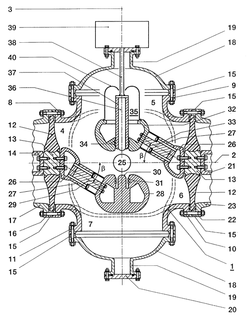
Fig. 1 shows a section through a schematically
illustrated housing 1 of this disconnector. As a rule,
the housing 1 is filled with an insulating gas under
pressure, sulfur hexafluoride (SF6) being particularly
suitable for this purpose. In order to assist clarity,
the visible edges of the housing 1 are only indicated.
As a rule, this housing 1 is at ground potential,
together with the other encapsulation parts of a metal-
encapsulated, gas-insulated switching installation. The
housing 1 has two axes 2, 3 which lie on a plane and
intersect at an angle a. As a rule, the angle a is
designed as a right angle but, for special
applications, angles other than a right angle can also
- 2 1 89322
- 4 - 95/133
be envisaged. As a rule, the housing 1 is cast from an
aluminum alloy in a pressure-tight manner. The housing
1 has at least four circular openings 4, 5, 6 and 7,
which are provided with flanges 8, 9, 10 and 11. In
this case, the flange 8 is assigned to the opening 4,
the flange 9 to the opening 5, the flange 10 to the
opening 6, and the flange 11 to the opening 7. The
openings 4, 5, 6 and 7 are arranged such that the axes
2, 3 pass through them at the center, to be precise the
axis 2 passing through the openings 4 and 6 and the
axis 3 passing through the openings 5 and 7. The
flanges 8, 9, 10 and 11 have surfaces which are
arranged at right angles to the respective axes 2, 3.
In this case, the opening 4 is closed by an
insulator 12, which is designed in the form of a disk
and has an electrically conductive cast-in fitting 13.
The cast-in fitting 13 is screwed to a conductor 14.
The insulator 12 is held by means of an outer ring 15,
in which grooves are incorporated for the accommodation
of sealing rings which are not illustrated. The outer
ring 15 is composed of two identically designed,
metallic, electrically conductive rings. The insulator
12 and the outer ring 15 are held in position by a
connecting flange 16, which is screwed to the flange 8,
of an adjacent housing 17. The opening 5 is in this
case closed by a cover flange 18. An outer ring 15,
which accommodates the necessary sealing rings (which
are not illustrated), is mounted between the cover
flange 18 and the flange 9. However, it is also
possible to dispense with this outer ring 15 and, for
this purpose, to provide the bearing surface of the
cover flange 18 or the bearing surface of the flange 9
with a groove for the accommodation of a sealing ring.
The cover flange 18 is provided with a connecting piece
19, which is closed in a pressure-tight manner by means
of a threaded cover 20. If required, a bursting disk as
well as connections for the gas supply of the housing 1
can be installed in the cover flange 18 or in the cover
20.
21 8~322
- - 5 - 95/133
The opening 6 is in this case closed by an
insulator 12 which is designed in the form of a disk
and has an electrically conductive cast-in fitting 13.
The cast-in fitting 13 is screwed to a conductor 21.
The insulator 12 is held externally by means of an
outer ring 15 in which grooves are incorporated for the
acco~o~tion of sealing rings (which are not
illustrated~. The insulator 12 and the outer ring 15
are held in position by a connecting flange 22, which
is screwed to the flange 10, of an adjacent housing 23.
The opening 7 is in this case closed by a cover flange
18. An outer ring 15, which accommodates the necessary
sealing rings (which are not illustrated), is mounted
between the cover flange 18 and the flange 11. However,
it is also possible to dispense with this outer ring 15
and, for this purpose, to provide the bearing surface
of the cover flange 18 or the bearing surface of the
flange 11 with a groove for the accommodation of a
sealing ring. The cover flange 18 is provided with a
connecting piece 19, which is closed in a pressure-
tight manner by means of a threaded cover 20.
The housing 1 and the closure parts described
above enclose an internal area 24 in which the active
parts, to which high voltage is applied, of electrical
switching devices can be installed, these being the
active parts of a disconnector, as already mentioned,
in this case. The covers 20 can be used for the
installation of the widely different accessories which
are used in metal-encapsulated, gas-insulated switching
installations. The housing 1 can also be provided with
additional connecting pieces, which can be used for the
installation of sensors and viewing windows for optical
inspection of the disconnector position. In Fig. 1, a
viewing window 25 is provided in the center of the
housing 1 and is installed in a cylindrically designed
connecting piece whose center axis runs at right angles
to the plane on which the axes 2 and 3 are located and
which, in addition, passes precisely through the
intersection of the axes 2 and 3. An identically
2~ 89322
- - 6 - 95/133
designed viewing window is provided in the opposite
wall of the housing 1, at precisely the same point. The
disconnection point of all disconnector versions is in
each case arranged centrally in the housing 1 such that
it can be inspected through the viewing window 25
described above.
Fig. 2 shows a simplified section through a
schematically illustrated first embodiment of an
electrical switching device, which is designed as a
disconnector for metal-encapsulated, gas-insulated
high-voltage switching installations, in the
disconnected state. This disconnector is designed as a
bus-tie switch-disconnector, as is provided, for
example, in the course of metal-encapsulated, gas-
insulated busbars. In this case, the conductors 14 and21 represent the respective ends of the busbar sections
which are at high-voltage potential. The conductor 14
is screwed to the metallic cast-in fitting 13 of the
left-hand insulator 12. An electrically conductive
angled connecting piece 26, which is designed to be
dielectrically favorable, is connected on the side of
the cast-in fitting 13 facing away from the conductor
14, and has a connecting surface which is inclined
through an angle ~ with respect to the axis 2. In this
case, the value of the angle ~ is 30~, but other values
of the angle ~ are also conceivable, corresponding to
the geometry of the housing 1, and an angle range of
from 25~ to 35~ can sensibly be implemented, as a rule,
for this angle ~. The inclined connecting surface is
screwed to a cylindrically designed spacer 27. The side
of the spacer 27 opposite the connecting surface is
screwed to a contact support 28. The spacer 27 extends
along an axis 29 which is on the same plane as the axes
2 and 3 and is inclined through the angle ~ with
respect to the axis 2. The contact support 28 is
designed in a dielectrically favorable manner and is
manufactured from metal. A cylindrically designed
mating contact 30, which i8 used as the fixed pre-
arcing electrode of the disconnector, is incorporated
2~ 89322
.
- 7 - 95/133
in the contact support 28. In addition, spiral contacts
31, which carry the current when the disconnector is
closed, are incorporated in the contact support 28. The
mating contact 30 extends in the direction of the axis
3, which at the same time forms the central axis of the
mating contact 30.
The conductor 21 is screwed to the metallic
cast-in fitting 13 of the right-hand insulator 12. An
electrically conductive angled connecting piece 26,
which is designed in a dielectrically favorable manner,
is connected on the side of the cast-in fitting 13
facing away from the conductor 21, and has a connecting
surface which is inclined through an angle ~ with
respect to the axis 2. Care must be taken in this case
to ensure that these two angles ~ always have the same
value. The value of this angle ~ in this case is
accordingly likewise 30~. The inclined connecting
surface is screwed to a cylindrically designed spacer
27. The side of the spacer 27 opposite the connecting
surface is screwed to a contact support 32. The spacer
27 extends along an axis 33, which is on the same plane
as the axes 2 and 3 and is inclined through the angle ~
with respect to the axis 2. The axis 33 runs parallel
to the axis 29.
The contact support 32 is designed in a
dielectrically favorable manner and is manufactured
from metal. Spiral contacts 34 for carrying the current
are incorporated in the contact support 32. The moving
disconnector contact 35 is arranged in the center of
the contact support 32. The moving disconnector contact
is designed cylindrically and its axis coincides
with the axis 3. The moving disconnector contact 35 has
a switching pin 36 which is surrounded by a contact
tube 37 of tubular design. When the disconnector is
connected, the contact tube 37 makes contact, after the
switching pin 36, with the spiral contacts 31 of the
contact support 28 and, during disconnection of the
disconnector, the contact tube 37 i8 released first
from the spiral contacts 31 of the contact body 28, and
21 ~322
- 8 - 95/133
the switching pin 36 is thus released from the mating
contact 30. An insulating rod 38, which is operated by
a drive 39, sets the moving disconnector contact 35 in
motion. The drive 39 is mounted on the upper connecting
piece 19. The drive 39 has a speed-controlled DC motor
whose rotor is fitted with permanent magnets. The
control instructions for the speed-controlled DC motor
are generated by a superordinate control system which
is not illustrated. The insulating rod 38 is passed out
of the housing 1 in a pressure-tight manner. The
insulating rod 38 is moved by the speed-controlled DC
motor via a lever drive, and a rotating bushing is
used, as a rule, as a pressure-tight bushing. The side
of the moving disconnector contact 35 facing the drive
39 is covered by a shield 40, which is designed in a
dielectrically favorable manner and is composed of an
electrically conductive material. The moving
disconnector contact 35 extends along the axis 3 which,
at the same time, forms the central axis of this
contact. The spiral contacts 34 surround the contact
tube 37 and connect it to the contact support 32 in an
electrically conductive manner.
When the disconnector is in the connected
state, the current flows from the conductor 14, through
the cast-in fitting 13, the angled connecting piece 26,
the spacer 27, the contact support 28, the spiral
contacts 31, the contact tube 37, the spiral contacts
34, the contact support 32, the spacer 27, the angled
connecting piece 26 and the cast-in fitting 13 into the
conductor 21.
Fig. 3 shows a schematic illustration of the
profile of the disconnection movement s of the
switching pin 36 as a function of the time t. The
movement of the contact tube 37, which is intended to
carry the rated current, will not be considered any
further here. The closed disconnector receives a
disconnection instruction at the instant To. The
disconnection movement of the switching pin 36 start~
shortly after this, at the instant T1. The drive 39
21 89322
.
_ 9 _ 95/133
accelerates the switching pin 36 to an increasingly
great extent until the contact disconnection between
the switching pin 36 and the mating contact 30 takes
place at the instant T2. The switching pin 36 is
accelerated even further until it reaches its maximum
speed. In the case of this disconnector, for example,
this m~;mll~ speed is in the region of 300 m~m/s, but
generally is somewhat above 300 ~m~/s, and the speed of
330 mm../s has proven to be particularly favorable.
Shortly after reaching this maximum speed, the
switching pin 36 is braked again so that, from the
instant T3, it continues to move at a slower speed in
the disconnection direction, this speed being in the
region of 50 ~m~/s. ~owever, after the instant T4, the
switching pin 36 is accelerated more sharply again, to
be precise to a speed of about 300 ~m~/s. Shortly before
reaching the disconnected position, the switching pin
36 is braked again, and then runs into the definitive
disconnected position at the instant Ts.
Fig. 4 shows a schematic illustration of the
profile of the speed v of the switching pin 36 as a
function of the ti~me t during the disconnection of the
disconnector. This illustration likewise shows the
three essential speed ranges A, B and C of the
switching pin 36 which have been described in
conjunction with Fig. 3. The range A comprises the time
interval between T2 and T3, the range B comprises the
time interval between T3 and T4, and the range C
comprises the time interval between T4 and Ts.
The comparatively high ma~;mllm speed in the
region A brings with it the advantage that only a
comparatively short time interval r~m~; ns for the
restrikes which may occur in this region A as a result
of so-called loop current switching operations. The
life of the switching pin 36 and of the mating contact
30 is advantageously lengthened as a result of this
advantageous limiting of the possible nu~mber of
restrikes and a reductlon in the erosion llnked
thereto, and this results in a considerably increased
21 ~9322
.
- 10 - 95/133
availability of the disconnector. In the case of a
switching installation which is provided with a double
or multiple busbar system, loop current switching
operations are understood to be operational changeover
operations, under load, from one busbar system to
another, which are carried out with the assistance of
the disconnector.
The comparatively low speed in the region B
brings with it the advantage that, when capacitive
currents are being disconnected, only a comparatively
small trapped charge rc~-;ns in the metal-encapsulated,
gas-insulated high-voltage installation after passing
through this region B. Capacitive residual charges
which remain on the active parts of the high-voltage
installation are called a trapped charge. These
residual charges are dissipated to a considerable
extent by restrikes, which occur in the region B,
between the mating contact 30 and the switching pin 36.
These residual charges also influence the size of the
transient overvoltages, that is to say the smaller
these residual charges are, the smaller are the values
of the transient overvoltages to be expected, as well.
However, the speed of the switching pin 36 in the
region B should once again not be so slow that the
number of restrikes occurring in this region becomes
too great, since each of these restrikes causes
corresponding compensation processes and thus
undesirable sharp voltage spikes as well (VFT, very
fast transients).
In the region C, the switching pin 36 is then
once again accelerated to a comparatively high speed in
order that the position of the switching pin 36 which
corresponds to the full disconnection travel is reached
as quickly as possible, that is to say that distance
between the switching pin 36 and the mating contact 30
which withstands any voltage spike occurring in the
relevant metal-encapsulated, gas-insulated switching
installation. The switching pin 36 has reached its
- 21 ~q322
- 11 - 95/133
definitive disconnected position at the time Ts, and it
has moved through its full disconnection travel.
During connection of the disconnector, the
moving disconnector contact 35 is moved by the
insulating rod 38, which is operated by the drive 39,
along the axis 3 toward the fixed mating contact 30.
Any pre-arcing between the switching pin 36 and the
fixed mating contact 30, which may be caused by
residual charges and/or by an operating-frequency
voltage being present between the contact support 32
and the contact support 28, is coped with correctly by
the disconnector. As a result of the geometrical
arrangement of the disconnector active parts, it is
impossible for any spreading of the pre-arcing arc to
occur toward the wall of the housing 1. The drive 39 of
the disconnector is designed such that it moves the
moving contact arrangement 35 reliably into the
intended connected position in every possible
operational case, so that this always ensures that the
current is carried correctly via the contact tube 37,
which is intended for this purpose, and the spiral
contacts 31 and 34. As a rule, when a disconnector is
being switched on, it is desirable for the speed of the
switching pin 36 to be as high as possible throughout
the entire connection process, but the stepping of the
connection movement, which would likewise be possible
per se, is not used in the case of this electrical
switching device, since it would physically be
pointless.
This drive principle, which is used here for a
disconnector and optimally matches the movement profile
of the switching pin 36 to the physical characteristics
to which disconnector switching processes are subject,
can, of course, also be used, appropriately modified,
for other switching devices and other switching
processes. In this case, power circuit breakers having
non-uniform contact movements can primarily be
envisaged, and, in particular, it i8 al~o conceivable
for different contact movements to be provided
21 ~39322
- 12 - 95tl33
depending on the switching operation to be carried out.
For example, when small inductive currents are being
disconnected in the case of a puffer circuit breaker,
the disconnection movement could take place so slowly
that the blowing of the arc takes place sufficiently
smoothly that the arc is prevented from turning off
before the zero crossing, so that no overvoltages
caused by the turning off can occur and there is
therefore no need to provide protective measures
against such overvoltages, the advantageous consequence
being considerable reduction in the cost of the
switching installation in which this power circuit
breaker is used. In the case of power disconnection,
the same puffer circuit breaker would, however, operate
at a comparatively high contact speed in order to
produce the necessary gas pressure for blowing out the
arc in the shortest possible time in a conventional
piston-cylinder arrangement.
The movement sequences of switching devices can
advantageously be matched to the physical
characteristics of the corresponding - switching
operations in all areas relating to distribution of
electrical power, that is to say at all voltage levels,
in open-air and encapsulated switching installations as
well as in DC and AC power supplies. The influences of
different insulating and/or quenching media, for
example of liquid or gaseous media, could also be taken
into account in a very simple manner with respect to
the optimal matching of the contact movement.
Obviously, numerous modifications and
variations of the present invention are possible in
light of the above teachings. It is therefore to be
understood that within the scope of the appended
claims, the invention may be practiced otherwise than
as specifically described herein.
21 89322
- 13 - 95/133
LIST OF DESIGNATIONS
1 Housing
2, 3 Axes
5 4, 5, 6, 7 Openings
8, 9, 10, 11 Flanges
12 Insulator
13 Cast-in fitting
14 Conductor
10 15 Outer ring
16 Connecting flange
17 Adjacent housing
18 Cover flange
19 Connecting piece
15 20 Cover
21 Conductor
22 Connecting flange
23 Adjacent housing
24 Internal area
20 25 Viewing window
26 Angled connecting piece
27 Spacer
28 Contact support
29 Axis
25 30 Mating contact
31 Spiral contacts
32 Contact support
33 Axis
34 Spiral contacts
30 35 Moving disconnector contact
36 Switching pin
37 Contact tube
38 Insulating rod
39 Drive
35 40 Shield
a, ~ Angles
s Travel
t Time
v Speed
A, B, C Regions