Note: Descriptions are shown in the official language in which they were submitted.
21 8~458
GR 94 P ~304 P
Description i~l ~' ' F~
Kodular relay
The invention relates to a modular relay having
a base, in which plug-in connecting elements for at least
one load circuit, for one relay energizing circuit and
for one modular circuit are anchored, having a coil
former which is fitted with an el~_~L _ -t system with
a coil, core and armature and which i8 mounted upright on
the base, furth- ~ having at least one stationary
contact element and at lea~t one ving contact element
coupled to the armature, the contact ~1~ t~ being
connected directly to the associated connecting ~
which are anchored in the b~se, and having a printed
circuit board which stands uprlght on the base plane, is
fitted with the modular circuit and is electrically
connected to at least some of the connecting ~1~ tl3 of
the base.
For certain applications, for example in tor
vehicle e.ng; n^~ring~ relays for specific functions are
c ;n~ together with their drive circuit to form a
compact unit, a so-called module, in a housing having
plug- in connections, 80 that the relay can be replaced
together with its drive circuit in one action. Typical
examples are relays for flasher units, glow plugs and the
like. However, until now, the structural connection of
the relay system and the modular circuit which iB
~rranged on a small printed circuit board reguired a
relatively high level of _ _ 1~Y; ty since a specific
structure had to be developed for each application.
DE 30 05 460 Al ~ rlos^~ an elec~ tic
~witch having a ~ l l y modular structure of the type
n~t3 initially. Thi8 ig actually a E~p"C';f;C' refine-
ment as a glow-time relay which cannot directly be used
~or other ope~ational ~.-~J,oses. The
21 89458
-- 2 --
connections between the bal3e and printed circuit board
are not shown in detail; the connecting ~1~ t~ contain
round con- nectors which muat be ~eparately riveted into
holes in a connecting p~rt in the form of a board.
DE 33 06 019 C2 ~3;P~lo8~F a relay in which a
printed circuit board is ~rranged p~rallel to the base,
on the top of the m~gnet sy~tem. In this case, all the
electrical connections between the printed circuit bo~rd
~nd the base must be mad~ via conductor parts which are
in the form of bar~ and extend from the relay ~ystem at
the side, at right angles to the base plane. If high load
current~ occur, ~uch ~ ~L ~ . could leAd to heating
problems, since th~ switching cont~ct~ on the top of the
relay are also located in the r-gion of the printed
circuit board. The connecting ~1 r 1 q are al~o in this
case ~ d as round connectors which must be riveted
into the base on their own.
DE 38 34 413 Al fur~h~- _6 ~ 08e'2 the arrang-
ement of a relay on a printed circuit board, load con-
necting ~ t~ being arranged in the form of flat
connectors on the printed circuit bo~rd and at least some
of them being connected via a stamped grid to the other
c _ t~ on the printed circuit board. This is actually
not a plug-in module constructed on a b~e; i~stead of
this, the relay is only seated in addition to other
circuits on ~ relatively large prlnted circuit board,
which has to h~ve conventional printed circuit board
connections, t~eparately from the said load connectors.
Finally, US 4,400,761 ~;Re708-~ a compact relay
sy6tem, in the case of which a ba~e which is provided
with flat connectors is fitted with a printed circuit
bo~rd ~tanding upright. The relay i~ in this case not
mounted on the base, but with all the connection~ on the
printed circuit board, 80 that the load circuit must also
be routed via the printed circuit board to the base
connections. This not only results in heating problems
but
_ 3 _ 2 1 8 9 4 58
also reguires additional electrical conductor ~1~ tQ
nnd coDnecting points.
The aim of the present invention i8 to provide a
plug-in modular relay of the type mentioned initially,
5 which has a compact structure with as few parts as
poss~h~e and also m~kes it poss;hle to carry high load
currents without any problems. The 8~ L~.~ should
furt~ :e be ~l~si~n-d such that various applications
can be coped with using a single basic structure BO that
10 relays having different modular circuits can be pLc,l~cel
with a standard bas~ 8~-u~;L~LL6.
This aim is achieved according to th~ invention
ln that all the electrical connections between the
respective plug-in conn~cting elements ~nd the printed
15 circuit board ar~ formed by c-,..l-.u:Lc.. lements which ar-
loc~ted ~ ngsi~^ one another, are stamped integrally
with th~ir connecting ~1- tQ~ are arranged in nn
entirely or partially L~cessc~l manner in the top are~ of
the base and are connected to the printed circuit board
20 in a row, approximately at the same height, ~ n~Q;~, one
another in the vicinity of the lower edge of said printed
circuit board and in th~t the lower end section of the
printed circuit board rests on a side wall which rlms at
right angles to the base pl~ne and in whose region the
25 conductor ~1- t,Q, in each case form solder connecting
pins .
The modular relay according to the invention has
~ universal base design with a predet-rm;n~cl max;~
number of conductor elements which can be arranged
30 alongside one another on the top of the base or rcc~ad
in it, and all the connectors and connecting elements to
the printed circuit bo~rd nre available for dif ferent
modular relays havlng different contact systems and
dlfferent modul~r circuits. The individual conductor
35 elements are st~mped and pL~f-- I such that they in each
case form flat connectors, which emerge integrally toward
the bottom of the base in ~ desired connecting pattern,
~nd, at their other end, form solder pins which emerge
toward the printed circuit bonrd side. If a modular rel~y
_
- ~ 21 89458
-- 4 --
tog~ther with its modular circuit require~ less than the
mAximum number of connection~ provided, then those
conductOr '?l r t-:l which are not re~auired can either not
be connected or can be omitted during the production of
5 the base, without the form or ~ y. t of the conduc-
tor elements which ar~ u~ed being ch~nged.
As has already been e~ ' initially, the
relay magnet 2~ystem is unted on the base, and the
contact Al^ tr; are connected directly to the associated
10 connecting ~1~ t~ . It is advAnt-Je~ 8 in this case for
the stationary contact ~ 'D to be ~ ni~n~d integrally
with th~ associated conductor elements, which at the same
time also form the plug-in connections ~nd the solder
connecting pin~. The power supply for a contact spring
which is connected to the armature i~ ~Yp~l; ently imple-
mented via a braid which is welded to the a~sociated
conductor element. The m~gnet ~ystem can be mounted on
the base via the contact elements and, if n~ce~ry, via
additional ~nchor points, which c~n be integrally f ormed
either on the plastic coil former or on one of the
metallic magnetic circuit parts, ~uch ~ on the yoke.
In an ^~ nt ref;r ~, it can fur~' ~ be
provided for the coil connections to be connected direct-
ly to the printed circuit board. In an adv~ntA~IeollR
r~f;~ t, a flange of the coil former in this case
form~ column-like supports in the top region of the relay
opposite the bal3e, which supports re~t on the printed
circuit board and from which ~upport~ coil connecting
pins emerge which are ~oldered into holes in the printed
circuit board. As ~ result of ~uch soldering of coil
connecting pins on top of the relay, the over~ll struc-
ture of the base, printed circuit bo~rd and relay is
given p~rticularly good robul3tnes23 and ~ nAl
consi~tency .
The conductor elements which are arranged in or
on the b~se can be mounted in slots on the base by
pl~g;n~ in. Where individual slots are ~nocc~ried in the
c~e of Bp'!tC'~ f; c ~ -;- t~ having le~3s than the
21 89~58
maximum nu~ber of conductor ~ , these slots can b-
closed, at least toward the bottom of the base, by the
plastic mat~rial of the base.
In another ~Te~;~nt r~f;~ t, it can be pro-
vided for ~t least some of the conductor elements to bein the insulating material of the base. It ia
poss;hl-~ in this case as well, for one '; t, for
conductor ~ which are not reguired not to be
inserted into the ld during the forming of the base,
10 for example in the case of plastic injection molding, as
a result of which their space is filled with plastic.
Mixed forms of ~ ' ';nrj ~nd plu~;nrj in are also
po~s;hle. Thus, for example, it is provided in an
~'Te~ nt rAf;__ ~ for the conductor elements for th-
15 connections of the modular circuit to be . -''~~ in the
base, while the conductor .~1~ t~ for the load connec-
tions are fitted E~hseSLU~n~ly~ by plugging in.
In order to couple the printed circuit board by
its lower edge region to the solder connecting pins of
20 the conductor Al- t~ it is, on the one hand,
advS~n~ u8 if the b~se forms ~ step in the
co~ ;n~ region 80 that th~ printed circuit board
rests against the vertical wall of this step; the solder
connecting pins of the conductor ^l~ ~ in this case
25 ~ e~ ntly emerge from t_e higher b~se section in the
region of this vertical wall and are thus soldered to the
printed circuit board directly in the region of the step.
The step thus 8; _ l;fie~ the t ;~ of the printed
circuit board on the connecting pins and, in particular,
30 firm seating of the connections is; ,_~,v_d. That part of
the base which is L~ce33~d ~ d8 by the step also
forms a bottom cover for the printed circuit board 80
that, as a result of the base edge being sealed with
respect to ~ housing cap fitted on it, the relay
35 ;nrl~ rj the printed circuit board is ~nrlosed in a
se~led manner.
On the other hand, the step makes the soldering
process somewhat more ~4;ff;cult since it must be covered
during wave-b~lth soldering. In order to avoid this
- 2 1 89458
problem
- 6 - 2 1 8 9 4 5 8
during soldering, a devD~ t of the invention provide~
for the base to be ~Dsi 3nDd in two parts, the stepped
part not being connected to the actual base, for example
by pl--s~i ng in, until ~f t~r the soldering of the printed
5 circuit board.
The said arL~y t of the solder connecting
pins in a row ~lnn~si~- one another can mean that all the
solder connecting pins lie on a common plane. Altern~-
tively, a mutual height of f set between these ~older
10 connecting pins is also guite conceivable within the
context of the invention, ~3 long as they are arranged
A l nn~ one another .
he invention will be DYpl~;nDd in more detail in
the foll -'n~ text uging - _l~ry _ n; t~l and with
15 reference to the dr~wing, in which:
Figure 1 ~hows a per6pective illustration of a relay
dule with the relay system con~:truct~d on n base and
with a printed circuit board which is indic~ted by
dash-dotted lines,
20 Figure 2 ~hows an exploded illustration of the base and
the individual parts of the relay from Figure 1 (without
the printed circuit board),
Figure 3 shows an ~ 1D~1 relay module with a housing
cap fitted on it,5 Figure 4 showE~ two sheet-metal p~nels with conductor
stamped out in groups, before being: ' - ''-' in
base,
Figure 5 shows a baE~e af ter extrusion coating with
: ' - ' ' ' conductor elements according to Figure 4,
30 Figure 6 showEI a base according to Figure 5 with addi-
tionally plugged- in c~. J,U~ L ~ r f or the lozld
connections of the relay,
Figure 7 shows a two-part base and
-
-- 7 --
Figure 8 shows a p6L."~,~ctive view of a somewhat '; f; ed
t of a relay module, in the stat~ before final
asse~nbly, with premounted individual ~~- ' lies.
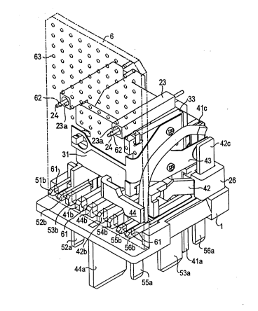
The relay module which is illustrated in Figure~
5 1 to 3 has a base l with plug-in slots 11 which are open
toward the top and contain ~_. L,,.~s, which cannot b~
seen, toward the bottom. An offset 12 in the form of
~tep is fur~ ~e integrally formed on one side.
A relay system constructed in a conv~n~;~n1~l
10 manner i8 seated on the base, with a coil former 2 as the
for a winding 21 and a magnet system 3. The
latter essentially comprises an angul~r yoke 31, a core
32 arr~nged within the coil and an armature 33, which is
in the form of a plate, is mounted on one yoke edge and
15 is pla~L..,ss~d into a rest position vi~ an arm ture
restoring spring 34.
The coil former has two fl~mges 22 on both sides
of the winding, which in each case form colu~nn-like
supports 23 on the top opposite the base 1. Coil con-
20 necting pins 24 are in each case anchored in thesesupports 23, approximately parallel to the plane of the
base 1. For support and - t;n~ on the base 1, the coil
former additionally has downward projecting pins 25 and
supports 27 as well as an ~ttachment 26, the latter at
25 the same time being used for guidance and tin~ of
station~ry contact elements 41c and 42c, which are still
to be de~cribed later.
A contact ~ ~, t for switching the relay
circuit in the present example comprises a stationary
30 make cont~ct element 41c and a stationary break contact
element 42c as well a8 a contact spring 43 which is
~1~8i~n~ as a c~nt;nl-~tion of the already ~ t;~n~d
~rmatur~ restoring spring 34. The statio~ary contact
~1~ tr3 41c and 42c are ~n;gn~cl integrally with in each
35 case one conductor element 41 and 42, r-spectively, which
are mounted in coL~ 3;n~ slots 11 in the
~ 21 89f~58
-- B
base 1 by plugging in. The conductor element 41 addi-
tionally has a flat connector 41a, which emerges at the
bottom through an opening in the base, and a solder
connecting pin 41b, which emerges, par~llel to the top of
5 the base, on the step wall 13; in a cc,~ in~ manner,
the conductor element 42 forms a flat connector 42a,
which is integrally formed at the bottom, and a solder
connecting pin 42b, which i8 inte~ral ly formed at the
side. A conductor element 44 is used as the connecting
10 element for the center contact spring 43 and forms a flat
connector 44a to the boottom of the baee and a solder
connecting pin 44 toward the step side wall 13. A con-
necting web 44c, from which the lo~d current is carried
via a braid 45 to the contact spring 43, is additionally
15 constructed on the conductor element 44. The contact
aLL~D~ t 4 could, of course, be modified, for example,
by providing only a break contact or ~ make contact; ~
bridge contact could ~1BO be impl~ t~, and it would
then be nr~--e-ry for the two st~tionary contact elements
20 41c and 42c to lie on a plane and for the contact spring
43 to be A~ n~d as a link without its own connection.
A module connecting a- ~,. t 5, comprising six
conductor ~ 51, 52, 53, 54, 55 zmd 56, is also
provided in the base. All these conductor ~ are
25 mounted in slots 11 in the b~D-e by pl~ in~ in, to be
precise in such a manner that they each form a flat
connector 51a, 52a, 53a, 54~, 55a and 56a, respectively,
to the bottom of the base, and a solder connecting pin
51b, 52b, 53b, 54b, 55b and 56b, resp~ctively, toward the
30 step wall 13. All the flat connectors on the bottom of
the base are arranged according to a predeter~li
pattern, while all the solder connecting pins in the
region of the step wall 13 lie alongside one another in
a row. These solder connecting pins, which are sta~nped
35 ~rom the relevant conductor elements, may dirrer slightly
in cross section, th~t is to say they have ~ larger cross
section for the load circuit and - in contrast to the
lllustr~ted ~ i t - m~ly ~1BO under gome circum-
stances vary in the height r~ t. Contact holes 61
.
21 89458
g
of the base 1 and its lower edge region rests on the step
side wall 13. In addition, in the region of the top of
the relay, the print~d circuit board 6 has two cont~ct
holes 62 for ~ ~' ting the coil connecting pins 24.
Further contact holes 63 are adv~n~ )usly used for
A- -' ting and n~king contact with further - _ - t~
for a dular circuit, which contact holes 63 cannot be
seen, in the same way as the conductor tr~cks.
During the as~embly of the modular relay, the
0 conductor ~1_ t~ 51 to 56 and the contact conductor
t~ 41, 42 and 44 ar~ firgtly plugged into the base
1 and, if appropriate, are fixed. After this, the coil
former with the magnet system is fitted and mounted.
Finally, the printed circuit board 6 is then plugged on
and soldered, at the side, via the module solder
connecting pins 51b to 56b, the cont~ct solder av~uL_Ling
pins 41b, 42b and 44b, ~nd via the coil connecting pins
62. In the region of their end resting on the printed
circuit board, the supports 23 in each case have a
conical r~cess 23a around the solder connecting pins 62,
80 that the solder cannot flow by c~p~ ry action to the
relay side of the printed clrcuit bo~rd. Fur~h~ c, the
cutout is used for tolerance -, rAtion and thus
simplifie~ the assembly of the printed circuit board.
Plugging a housing cap 7 onto the base 1 pro-luces a
cloEled housing, which can be sealed at the lower edge
region. The lower edge of the prlnted circuit board 6 is
also covered by the offset 12, which is in the form of a
~tep .
In the case of the ~ ' -';- t which has been
described 80 far, all the conductor ~1A tl9 have been
mounted in the base by pl~ ;n~ in. If it is ;nt~n~l^d to
use less than the maximum shown number of nine c.,~- lu~ Lor
in an '~'; t, the Col ., ,J~ ;n~ ~_ Lu~ca
for the flat connectors can be filled, or closed toward
the ~ r~th by ~ sprayed skin, even durlng the produc-
t lon of the b~ae .
A further - ' - '; t of ~ ~ase is shown in
Plgures 4 to 6 in various phases o~ production,
lo 21 89458
some of the Cu~du~L~L elements being ~ in the
plastic of the base. An: ' ~'i t is shown in which the
conductor ~l t~ c~n be obtained by as few individual
steps al3 possible. In this case, as is illustrated in
Figure 4, three conductor ~l~ t.~ 81, 82, 83 or 84, 85
and 86, respectively, are each obtained from in each case
one sheet-metal panel. The flat connectors 81a, 82a and
83a of one sheet-metal panel and 84a, 85a ~nd 86a of the
other sheet-metal panel in this case each lie on a plnne,
while the top sections of the conductor ~l ~ tQ are in
each case cut, angled and bent such that the ~older
connecting pins 81b, 82b, 83b, 84b, 85b and 86b which are
formed at the ends all lie in a row.
The conductor elements on ~ panel are initially
in each c~se connected to one another via webs 87 80 that
only two sheet-metal p~rts need be inserted into the
in; ection mold. A base 91 according to Flgure 5 i~ now
formed by extrusion coating the two panels, the dimen-
sions of which base 91 co~ y~ d to those of the base 1
in Figures 1 and 2, only the module connecting elements
already being ' -''-~. The ;nt- ';Ate webs 87 are then
cut through oo that the individual conductor ~- tl'3 are
electrical- ly insulated from one another. Fur~ e,
the baEle 91 all3o has plug-in slots 92 for ~~ ' ting
the conductor ~ 41, 42 and 44 with the cont~ct
for the load circuit. These are ~ n~d a~
shown in the example in Figure 2 and are plugged in in
the ~ame manner as there. A base shape according to
Figure 6 is thus obtained. ~he coil former 2, with the
magnet system 3, and the printed circuit board 6 can then
be mounted on this populated base as in the previous
example .
Figure 7 describes a ';fi~tion in the form of
a two-part base. The base 101 which is illustrated there
c~ L~y~ dt3 to the base 1 in Figures 1 and 2 with the
exception that, instead of the step or the of f set 12
there, this is formed by a separately manufactured second
base part 102 which is in each case snApped by means of
side ~rms 103 onto l~t~ h;n~ tabs 104
- 11 2189458
of th~ base 101 and can be mounted in this way. However,
the base 101 is initially populated without the second
base p~rt 102 in that, as in Figure 2, the conductor
~1~ t ~ shown there are plugged into the slots 111. The
5 printed circuit board 6 from Figure 1 is then placed onto
the side wall 113 and i~ plugged onto the solder
connecting pin6 of the conductor Pl~ t~;. The printed
circuit board can then be soldered easily, without any
pro~ecting base step. After this, the second base part
102 is plugged with the said side arms 103 onto the base
101. The base parts 101 and 102 now form a closed bottom
p~rt which, together with the c~p 7, forms a clo~ed
housing. If n~c~ y, the joint between the b~se p~rts
101 and 102 can also be ~ddition~lly sealed, with the
edge gap between the b~se and cap. This two-part con-
struction of the base c~n, of course, ~180 be used if the
conductor ~lements are at least p~rtially ~ d, a8 is
shown in Figures 4 to 6.
The relay module which is illustrated in Figure
8 has a base 201 with plug-in slots 211 which are open at
the top ~nd contain ~ Lu~ ;~B~ which cannot be seen, at
the bottom. Seated on the b~se is a relay sy~tem having
a coil former 202 ~8 a mounting for A winding 221 and a
magnet system 203. The latter essentially comprises an
angular yoke 231, ~ core which is aL.~yed within the
coil ~nd an arm~ture 233 which is in the form of a plate,
18 mounted on ~ yolce edge ~nd ~ 8 ~ e~ !eEOd into a rest
pos~ tion via ~n armAture restoring spring 234 .
Conductor ~1, t n 241 to 246 are anchored in the
base in the ~_L l,UL_EI 211 which are only partially Vi8-
ible; further lines ~re only parti~lly vi~ible. A flat
connector 241a, 242a etc. which emerges at the bottom is
integr~lly formed on each of the conductor ~ . In
addition, each conductor element has a solder connecting
pin, for example 241b, 242b etc., which pro~ects horizon-
tally beyond the side w~ll 213. Most of these
12 - 2 1 89458
solder connecting pins are located ~ ng~ one anoth~r
in a straight row; spe~-if;c solder connecting pins, for
exampl~ the solder connecting pin 243b or th~ solder
conn~cting pin 246b, are ~dmittedly located in the gap
5 between two adjacent solder connecting pins, but are
offset upward somewhat in height in order to obtain a
gr~ater insulating separation. A stationary make contact
elem~nt 246c is integrally formed, 8tanding upright, on
the conductor element 246. In addition, the con.h,. l.o~
elem~nt 243 has ~ connecting web 243c which ext~nds
transversely over the base surface and to which a braid
247 is welded, which carries the load current to a
contact spring 248. This contact spring 248 is connected
to the armature 233 and is integral with the restoring
15 spring 234.
On the side f~cing away from the armature, the
coil former 202 has a som~what raised coil flange 222 in
which coil connecting pins 223 Are ~hoLL~. These coil
connecting pins are angled such that th-y form solder
20 connections par~llel to the solder connecting pins 241b
to 246b. In addition, T-shap~d spring lugs 224 are
integr~lly formed on the, '~ - th of the coil former,
opposite which gpring lugg 224 there are CG..~ ;n~
latching wedges 214 on th~ bas~. A latching hook 215 is
25 furth~ -re integrally form~d on th~ base in th~ vicinity
of the side wall 213, opposite which l~tching hook 215
there is a co~ ;ng latching window, which cannot be
seen, on the ~n~ n^~th of th~ coil flang~ 222. When th~
coil form~r is b~ing unted on the base, the latching
30 lugs 224 slide with their side arms over the latching
wedges 214 and latch in behind them ~t the end of the
fitting ~ t. At the same tim~, the latching hook 215
latches in the said l~t~-h;n~ window in the coil former on
the opposite side, 80 that the b~se and the coil former
35 ar~ attached to one another in a force- fitting and
positively locking manner.
A printed circuit board 206 is fitt~d, standing
upright with r~sp~ct to the bas~ plane, to th~ base 201
which is - ' ;necl with th~ magnet system, to b~ precise
~ 21 89458
- 12~ -
to the side urface 213. Contact holes 261 and 262 are
provided in the printed circuit board 206, in the vicin-
- ity o~ its lower edge, in a row cc,.~ ; n~ to the
~older comlecting pin~
- 13 - 2 1 89 4 5 8
241b to 246b. The contact holes 262 are in this case
offset somewhat upward from the straight row of contact
holes 261, in the same way as the somewhat raised con-
necting pins 243b and 246b, in order to ensure the
already described, incr-ased insulating separ~tion. In
addition, the prlnted circuit board 206 has two contact
holes 263, which match the coil connecting pins 223, in
the region of the top of the magnet system 203. After the
printed circuit board 206 has been fitted, it is soldered
10 to the solder connecting pins in the contact holes 261,
262 and 263, as a result of which the magnet system and
the conductor elements which are anchored in the base are
connected to a circuit, which cannot be seen, on the
print~d circuit board 206.
Finally, an addition~l b~se pArt is plugged onto
the side surface 213 of the base 201 by means of attach-
ment pins 213. The bottom of the printed circuit boArd
206, which was previously exposed for soldering, 18
covered in this w~y. It is thus poss~hle to form a closed
20 housing by plv~n~ a housing cap, which is not illus-
trated, on the base 201 with the additional part 212,
which closed housing can be sealed on the l~n~ n~Ath by
filling out c~rilla~y ~oints.
The maximum nu~nber of conductor ~lements are
25 shown in e~ch c~se in the ~ described, six addl-
tional connectlons for the module thus being provided in
each c~lse in ~ddition to three load connections. Depend-
ing on the ~pplic~tion, these additional connections can
be allocated to co _L~ d to the modular circuit. If ~11
30 the connectlons are not re~uired, the c~ ....A~n~
conductor ~1 ~ t~ can algo be omitted during production
of the base, or it is possible to cut off connectors
which are not required before or after t~n~ in the
base .