Note: Descriptions are shown in the official language in which they were submitted.
~8~
This i~ a divi~ion of applica~ion No. 2, 048,385
filed August 2, 1991.
SYSTEM ~J..1~O~ ; pr~Orr~AM7~ARrr' IMPLANTABI,E TRANspoNDER
BACKGROUI~D OF THE INVFNTIO!~
~ This invention is directed to a passive transponder and,
in partieular, to a passive trAnCp~r~ r whieh is programmable after
completion of manufacture utilized for monitoring the
characteristic of the host into which it is embedded, and more in
particular for identifying an animal and its characteristics.
Transponders and scanner systems are well known in the
art. These systems inelude an interrogator which transmits and
receives signals from a passive transponder. One such use is a
trAnCpnn~l~r ?~D~ in an animal. The prior art system known from
U.S. Patent No. 4,730,188 includes an antenna which transmits a 400
KHz signal which is received by the transponder ~ d in the
animal and returns a divided signal of 40 ~Iz and 50 KHz. This
signal is eoded in accordance with a combination of 40 K~z and 50
~z portions of the transmitted signal to eorrespond to a
prepL.yL 1 ID number stored in a chip eontained within the
passive trAnCp~n~-r. The ID number is preprogrammed at the time
of ~m-f~Aetllre~ This ID number allows identifieation of the animal
in whieh the l LAn~ r is ~ ed. The seanner then inputs this
coded ID number into a mi-Lc~ er for processing.
The prior art transponders have been less than completely
satisfactory beeause the amount of information whieh may be
transmitted thereby was limited to the pL~:~L~L ?d identifieation
numbers eontained thereln. Aeeordingly, in a eontemplated use sueh
as animal id~nt~f~c~tion, the user must use the l.L~L~L -'
identifieation number to identify the test animal. However,
identification numbers are usually used as shorthand manner for
pr~c~nt~nlJ data l-rn,-~rn~nq the animals. This requires that the
user mateh his animal information to the preassigned trAncprn~l~
identifieation number resulting in an inerease of time and effort.
Additionally, this prior art deviee is unable to automatieally
transmit system status information, such as museular pressure or
temperature of the animal. Aeeordingly, the amount of information
transmitted is quite small.
Beeause the transponders divide the reeeived signal, a
high fregueney reeeived signal must be broadeast to the tL~ vl.der
so that the divided signal will have a high enough frequency to
, . .... , , _ , _ _
2189~61
transmit information. These higher frequencies are regulated by
the FCC, therefore, the amount of power which can be supplied to
the trAn~p~ r, and in turn the read distance is limited.
Additionally, because the trAn~p~n~7Ar transmit antenna operates at
40 KHz, it is subject to background noise interference from
television monitoring screens or computer CRTs which by necessity
are normally present since they are used in conjunction with
miuLu~Lucessol~ which are used during Srlnnin1. These monitors
also operate utilizing a 40 ~Hz and 50 KHz RF signal. 8ecause
these monitors have a high power output relative to the antenna
they int_rfere with the operation of the intsrrogator when the
interrogator i8 used in proximity to ~ _LeL, and other various
monitors .
Therefore, a passive tr~ Ar which simultaneously
senses an environmental condition and transmits this information
along with user P1UYL hle identi~ication information in a manner
which is less susceptible to ba- Iw,Luu..d noise interference is
provided by the instant invention.
STlMMARY OF ~ INVENTIOn
Generally 6pAAk~n~, in accordance with the instant
invention, a passive l..A~ Ar which identiries, simultaneously
senses and transmits a condition to be sensed, such as the intern~l
temperature or the llke of an object ig provided- The t~A"~IJ ~
includes a receive antenna for receiving the interrogator signal.
The LL~)'`*1"''"1- ~ 1S driven by the i~lL~LLo~atUr signal. A sensor
circuit d~F-~?~ within- the tr~nsp~n~lDr - ~_5 the condition to
be sens_d Or an animal in which the t__r ~ --r is . - -1- A
data ~ ..e.v~r rec_ives the interrogation signal and enables the
sensor circuit to output a signal representative Or the condition
to be sensed. The data se~ an Ar causes the signal representative
of thQ condition to be output over a transmit antenna contained
within the tr~n~ron-lAr.
In one: 'i L of the invention, the trAr-~ lnr also
includes a ~UU,L hle memory circuit which may be p~u~ with
a user s~Al ectA~l identification code through use of a signal
received by the tr~n~p~n~Ar. The data ~eT1 -- r enables both the
sensor circuit to output the t~ tuL~ and the ~r le
21~ 6I
memory to output an identification code in sequence. A frequency
generator and modulator is provided for receiving the signal
representative of the condition to be sensed and the identif ication
code and modulatirLg the data to be output on an output carrier
signal in response to the lnput signal. The output signal ~re~uency
i8 independent of the input signal frequency which may be less than
1 ~ ~z .
The invention will now be described further by way of
example and with reference to the ~ ying drawings.
8RIEF n~ccl~Ip~ 9F I~IE I)R7`'~I~GS
FIG. 1 is a block diagram of an interrogator constructed
in accordance with the invention;
FIG. 2 is a block diagram of a passive transponder
constructed in accordance with the invention;
FIGS. 3a, 3b are respective halves of the frequency
~nrr~ r and modulator of FIG. 2 constructed in accordance with the
invention;
FIG. 4 is a circuit diagram for a data sequencer
Wl~ LLu~Le~ in a~ uL~ with the invention;
FIG 5 is a circuit diagram o~ the one time ~ L hle
memory constructed in accordance with the invention;
FIG. 6 is a side elevation view of a transponder
constructed in accordance with the invention;
PIG. 7 is a top plan view o~ a tr~n~r~-n~r constructed in
accordance with the invention;
FIG. 8 is a sectional view taken along line 8-8 of
FIG. 7; and
FIG. 9 is a sectional view taken along line 9-9 of
FIG. 7.
-
218~6~
4
DE~rATTT~n U~ ON OF ~ k~ RI ~ T~MR~DIMrA~TS
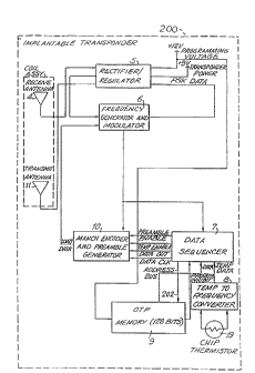
Reference i5 first made to FIGS. 1 and 2 in which block
diagramc of an exciter/receiver (ninterrogatorn) lOO ~nd
i~plantable passive ~ r (n~l-nA~ Arn) 200 are provided.
Interrogator lOO transmits an exciter signal to L-~ 200.
The exciter signal i5 received by LLA~ r 200 and powers
trAncrnn~r 200. Oncs energized, LLA"~ 200 i5 caused to
output a data signal . q his data signal includes a preamble
portion, t~ - ., data and i~nt~f1~-ation code. The data signal
is a PSX (pha~e shift keyed) signal with a 455 KEz carrier
frequency. The LL 1c~Ainn i8 a cnntinl~n~Q~ cyclic data stream
C~I1~A1n;nq the ~ ID and t ~LUL~ information. Th18
information is received by interrogator 100 and is ~ ted,
translated and input to a host computer for proc~cc1n~.
As will be described in greater detail below"L~ r
200 1 n~-lv~?~c a one time ~L0YL ~ memory 9 . PL~L 100
which is coupled to a host co~Dputer receives an identification code
that is to be LIL~YL ~ into I .A. ~ ~r 200. IntelL~AtoL lOO
modulates the amplitude of the excitation signal to _ ~Aate
with LL-nAl~ 200. When LLA"A1J'~ 200 is in a progra~ Dlode
~g~61
.
s
one time ~ru.~, hle memory g may be ~JLU~L - ~ by interrogator
100.
In an exemplary embodi~ent, interrogator 100 c~ tes
with trAncr~n~l~r 200 through inductive rol-rl 1nq known in the art
from ~ S Patent No. 4,730,188. The interrogatiom
signal is less than 10 KHz and more precisely ~109 Hz. The return
data stream output by the tr~nCp~n~l~r is output on a higher
frequency carrier signal of 45s ~CHz.
A mûre detailed description of the invention is now
prûvided. Description is made of the system in which transponder
iûo already has been programmed and a user selected identification
code has been stored in one time ~LCYL hlc memory 9.
Interrogator lOo includes a frequency generator 1 which outputs a
7109 Hz signal. A power amp 2 receives the output signal and
causes the signal to flow through the primary coil of a transmit
antenna 3 which generates an excitation field at a frequency of
7109 Hz from exciter 100.
Reference is now made crec~f1r~lly to FIG. 2 in
cnnnP~~ti~ n with de5cribing the internal configuration of
tr~nCp~n~r 200. A receive antenna 4 mounted within tr:~ne:p~nrl~r
200 receives the exciter signal from interrogator 100 and inputs
a 7109 Hz signal to a rectifier/regulator 5 . r - ; f 1 ~r/regulator
5 receives the AC signal from the receive antenna and rectifies the
signal. The unregulated voltage is then regulated to 3 volts to
power the digital circuitry cnnt~inod within t~ A~r 200. In
an ~ r ~, r~r~i f~r/r~ tor 5 ut~ l 1 7~c Schottky
diodes to reduce the voltage drop. Ps~t~f~r/regulator 5 limits
the voltage to protect the digital electronics. The rectified
signal i8 then passed through a r~e~ue~;y ~ dt-,r modulator 6 and
input to a data ~c~len~ r 7 and manchester encoder and preamble
generator 10.
Data ~eqt~nc~r 7 receives as inputs the 7109 Hz signals,
têmperature data from a tempera~ure to r-~ uè~ y converter 8 and
the ~ ID data from one time p..,_ hle memory 9 and
controls the seq~nc1r~q of the cyclical transmitted data stream
which in~lud.~t: the preamble, ID data and f' ~ uLè data. A one
time ~roy. `-lf- memory g stores the ID data therein. When data
-
2189461
sequencer 7 receives the 7109 Hz input signal, it first outputs a
preamble enable signal causing manchester encoder and preamble
generator 10 to output a data preamhle. It then outputs the ID
data stored in one time p~U~L -hle memory 9. Data s~qu~nr~r 7
sequentially aCC~c~C the address to be read from memory 9 through
address bus 202 this causes memory 9 to output the data to data
sequ~nr~r 7 which gates the data and outputs the ID data at the
appropriate time to ~anchester encoder and preamble generator 10.
Reference is now made to FIG. 4 in which a circuit
diagram of data 6equencer 7 ls presented. Data s~ nr~r 7
includes a counter 700 which receives the 7109 Hz signal, divides
by 16 and outputs a 444 Hz signal. One time ~L-JyL hle memory
9 outputs a program inhibit signal indicative of whether the memory
has been plV~L -' by the user with an ID data. The program
inhibit signal has a value of O if the memory has already been
programmed and a value of 1 if it has not been prc~L -~. A ~irst
NAND gate 704 receives the 7109 Hz signal output by frequency
generator and modulator 6 as a first input and the inverted program
inhibit signal as a second input. A second NAND gate 706 receives
the 444 Hz clock signal and the program inhibit signal as inputs.
The outputs of both NAND gate 704, 706 are input to a third NAND
gate 708 which gates each Or the outputs and produces a clock
signal having a value of either 444 Hz or 7109 Hz as an output.
- A binary counter 710 receives the output of NAND gate 708
and utilizes this signal as the ;nt~rn~l timing signal. Binary
counter 710 provides a data clock at its output Q1 of 3555 Hz when
a signal o~ 7109 Hz is received. E~inary counter 710 also
sequentially -r~aa~C the ad-lL~sses within pLl~L hle memory 9
through the address bus at this clock rate.
During the reading of data from memory 9, the ~r-~cc~n~
of each memory causes ID data to be output by memory 9. This data
is then input to a clock 718 which receives as a clock input the
3555 Hz data clock output by binary counter 710. This is to
synchronize the data being output by memory 9 with the transmit
seq l~ne as Le~e se..ted by the data clock.
A NAND gate 714 and a NAND 716 are provided to gate the
tr:~n~iccion of the preamble, ID data and t~ ~ ~I,UL~ data portions
of the cyclical transmitted data stream. NAND gate 714 receives
~8~6~
the output of Q8 as one of its inputs and the output of Q9 as its
other and outputs the preamble enable signal. NAND gat~a 716
receives the inverted output of Q8 and the output of Q9 and outputs
the temperature enable signal so that the two NAND gates will not
enable the tr~n~ esion of the respective data simultaneously.
Additionally, a NAND gate 720 utilizes the preamble enable signal
to gate the temperature data being produced by temperature to
frequency converter 8 50 that when the preamble enable is low, the
temperature waveform is blocked.
During the read operation, the program inhibit signal has
a low value, therefore, its inverted signal is high. Because one
input of NAND gate 706 Ls O (the progran inhibit value), it will
continuously produce a high output. Whereas the inputs o~ NAND
gate 704 are a continuously high signal and the oscillating
waveform signal of the received 7109 Hz signal, the output of NA17D
gate 708 will be a 7109 Hz clock signal. Binary counter 710
utilizes this signal producing a data clock of 3555 Hz and a read
out rate of 3555 Hz.
In an ~ ry . ' - '~r t ~ i~ the output of Q9 is low
the preamble data is output and then the program ID data. Once the
value of Q9 goes high, the preamble enable goes high allowing the
t~ ur-~ data to be transmitted through NAND gate 720. During
the time Q9 goes high, the EPRON of memory 9 is still ~5eTl~nred.
However, the ID data is not output by the man~ aI encoder and
preamble generator 10.
To obtain the t~ LuLe data portion of the output
signal, a chip ~hormi~tor 19 il3 provided which outputs a r~ tan~ e
in ~ to ch~mges in temperature. The resistancQ is input to
temperatur~ to r.~ converter 8 which converts the r~e; e~ ~n~ e
to a rL. y~.en~;y which is input to data sequ~n~r 7. In an ~ y
L, t- ~.LuLa to rLt~u~ ;y converter 8 is an RC
oscillator that is controlled by the resistance of thermistor 19.
The frequency of the oscillator increases with temperature. The
oscillator has an approximate frequency of 160 KHz at 36-C. Data
8equ~n~ lr 7 gates this ~requency and outputs the signal to
manchester encoder and ~Le~ ' le generator 10 at the appropriate
time allowing manchester encoder and preamble generator 10 to
2189~61
output a cyclically tran5mitted data stream which ;nrl~ s the
preamble, ID data and te~perature/frequency data.
Manchester encoder and preamble generator 10 receives the
7109 Hz signal and ~,.} u--ds to the preamble enable, t~ tu~.:
enable signals, data out and data clock signal produced by data
se r1~nr~r 7 . When the preamble enable signal pL~ d~l~ ed by data
se~Pnr~r 7 is high it encodes the data being transmitted by data
sequencer 7. The 7109 }Iz clock is s~lect~d as the manchester clock
and the data out signal is always high producing an output twice
the normal data clock freguency. This allows a simple means of
detecting the beginning of the cyclical data s~ nre. In a first
fitage, the manchester clock is mixed with the ID data to produce
manchester encoded preamble and ID data signal. In a next step,
when the temperature enable signal i5 high, the manchester encoder
and preamble generator 10 replaces the manchester encoded ID data
with the temperature data completing one cycle o~ data
tr~nF~ n. This data is transmitted at 3555 baud to frequency
generator and modulator 6. By way of example, the preamble, ID
data and temperature data are pL.duced in this order. However, as
the entire output signal is continuous and cyclical, the
temperature data may be output f irst .
FLe~ y generator and modulator 6 receives the data to
be transmitted from manchester ~nro~l;n7 and ~L~ ' le generator 10
as well as the received clock signal of 7109 Hz. F~ .;y
generator and modulator 6 multiplies the input clock signal by 64
to produce a transmit carrier frequency of 455 KHz to output a 455
KHz carrler signal containing the data. This carrier signal is
phase shifted by 180 when the transmitted data changes st~te to
output a phsse shift keyed signal.
Reference is now made to FIG. 3a and 3b, wherein a
circuit diagram of frequency generator and modulator 6 is provided.
The circuit shown in FIG. 3a operates digitally on the received
7109 Hz signal and provides an input to an analog portion of the
circuit shown in FIG. 3b. The frequency generator and modulator
multiplies the frequency o~ the received clock (7109 Hz) to produce
a 455 KHz carrier signal by comparing an internal digitally
controlled oscillator with the period of one cycle of the received
clock signal.
=
21 89~ ~
.
An analog oscillator is provided having a capacitor 649
which i8 charged by a combination of voltage sources 630, 634, 638,
642 and 646 having values of i, 21, 4i, 8i and 64i respectively.
The current is input to capacitor 649 to charge. Capacitor 649 is
coupled to inverters 648, 650 arranged in series. The output of
inverter 650 is input to a MOSFET transistor 652 for discharging
capacitor 64g. This continuous charge and discharge provides an
oscillator o~ a certain freguency. The rate of oscillation is
based on the current sources so that the amount of charge stored
in capacitor 649 as a function of the amount of current and then
discharged by transistor 652 causes oscillations within the circuit
producing pulses at about 910 RHz. In an exemplary: '~';
capacitor 649 has a value of 10 pF.
The 910 XHz signal is input to a divide by 256 circuit
which includes NAND gate 610 and two binary counters 608, 612. The
910 KHz signal is input into binary counter 608 and is also one
input of NAND gate 610. The second input o~ NAND gate 610 is the
divided output Q3 of binary counter 608. The output of NAND gate
610 is input as the clock input of binary counter 612 so that the
output Q3 is a signal having a fre~uency of about 3554 . 68 Hz.
At the same time, the received 7109 Hz signal is received
by frequency generator and modulator 6 and is inverted by an
inverter 602. The inverted received signal is input to a flLp flop
604 as the clock input. Flip ~lop 604 is a divide by 2 80 that its
Q output is a signal having a frequency of about 3554 . 5 Hz . This
signal is aby~ hL~v~ls with the 3554.68 signal of the divide by 256
circuit. A NOR gate 618 receives the two signals as does a NAND
gate 616. A comparison is made between the two signals to
determine which occurs f irst and a~ u.- ~ L~ are made .
To prevent tog~l i n~ back and forth between one coming
before the other at NAND gate 616, a delay circuit is provided.
The delay circuit includes the flip flop 606 providing an input to
the flip flop 620. Flip ~lop 606 receives the 910 RHz signal as
the clock input and provides a Q output to flip flop 620 received
at the D input o~ flip flop 620. Flip flop 620 again clocks this
signal with the 910 E~z pulses of the oscillating clock formed
about capacitor 649. This delays the output of flip flop 620 by
at least one cycle of the 910 KHz pulse signal.
~8~61
A pair of NAND gates 624, 626 are provided. The output
Q of flip flop 604 representing the divided down received signal
having the 3554.5 Hz freguency is input to both NAND gates 624, 626
as is the delay Q output of flip flop 620. However, NAND gate 624
receives the inverted output of the divide by 256 circuit (the
3554.68 Hz signal) while NAND 626 receives the actual signal
itself. The outputs of NAND gate 624, 626 control are input to an
updown counter 628. The outputs QA-QD of updown counter 628
control the amount of current f lowing from each current source
through switches 632, 636, 640, 644 respectively to the capacitors
649 .
The relative outputs of NAND gates 624, 626 control
whether the amount of current fed to capacitor 649 should be
increased or decreased thus affecting the frequency of the pulses
produced. This is a delayed function 50 that no matter which
signal, the divided receive signal or the divided oscillator signal
goes high first it will be delayed before the gates 624, 626 are
able to determine whether the count o~ up down counter 628 should
go up or down. If the output Q of flip flop 604 goes high first,
it is delayed by flip flops 606, 620. If at the same time the
output at Q3 of binary counter 612 is low, the lnput of NAND gate
624 would be high while the input of NAND gate 626 would be low.
The output of NAND gate 624 would cause an up pulse at counter 628.
The counting of fllp flops 608, 612 are controlled by
flip flop 614 which receives the Q output of fllp flop 604 as lts
clear. Fllp flop 614 in turn controls the resetting of rlip flop~
608, 612 and thereby controls the output of the divide by 256
clrcult. Additionally, the clock input of ~lip flop 614 is the
output o~ AND gate 616. If the output Q3 is 1, th~ Q output of
flip flop 614 goes high causing output Q3 of flip flop 612 to go
low again restarting the whole process . ro~lnt; n~ can only occur
when the Q output of flip flop 604 is low.
I~ it is ~PtPrm~ nPcl by NAND gates 624, 626 that pulses
are not being output at 910 KHz corrections are made by updown
counter 628. Switches 632, 636, 640, 644 are analog switches which
allow the current from the respective current source 630, 634, 638,
642 to be output to the capacltor 649 to charge lt up at a faster
rate thereby increasing the ~ en~;y of pulses. As the need for
2~89~1
11
an increased frequency arises, the number of switches 632, 636 and
the like which will be turned on to allow current to pass to
capacitOr 649 increases sc~uentially until the frequency of the
pulses is sufficient.
A divide by 2 flip flop 654 receives the 910 I~z pulse
as a clock signal and outputs as a Q output a 455 ~Hz signal. The
455 ~IIz signal is the carrier frequency for the data which is
transmitted by tr~n~pon~1Pr 200. An exclusive OR gate 656 receives
the 455 E~Iz signal and the data to be transmitted including the
preamble, ID data and temperature data as a second input. The
exclusive OR gate shifts the phase of the carrier signal by 180-
in response to the data 50 that a phase shift keyed data output
signal is produced by exclusive OR gate 656. This phase shift
keyed signal is then transmitted to interrogator 100 where it i8
operated upon.
By multiplying the received clock by 64, a transmit
carrier freguency of 455 KElz is obtained. By digitally comparing
the period of 64 cycles of the internal digitally controlled
oscillator with the period of one cycle of the received clock, a
very inaccurate frequency source can be synchronized with a very
accurate r~u~ y source to produce an accurate carrier rL~uU~ y
at a much higher frequency without imposing limits on the frequency
values. As ~ cl~lced above, this is ~ Sh-~cl by ~7~t~rm1n;
whether the received clock cycle is shorter or longer than the 64
cycles of the o~cillator. If the received clock cycle is shorter,
then the oscillator ~L~:~u~ ;y is too low and a up pulse will be
generated output to an updown counter controlling the current
sources to the capacitor. Ir the received clock cycle i5 longer,
then the oscillator rL~:~u~ ;y is too high and a down pul~e is
generated and output to the updown counter.
The pha~e shi~t keyed data is output through
rectifier/regulator and a transmit antenna 11. A 455 K~z field i8
-luced which iEi received by receive antenna 12 of interrogator
100 .
The received signal is input into an i _ - n~ e buffer 13
which buffers the high ~ n~ e of the tuned receive coil forming
receive antenna 12 80 that the much lower i ---n,e Or the receive
filter doe~ not reduce the received signal strength. The ;rre~i In~ e
, _ _ _
- 2I89~61
12
matched signal i8 an input to a receive filtering and amplification
circuit 14. Receive filter amplification circuit 14 fllters out
unwanted signals and amplifies the received signal for further
proces6ing .
In an eypmrlAry ' ~ L, receive filtering and
amplification circuit 14 uses a multiple pole ceramic band pass
filter with a +/- 15 ~Hz pass bandwidth and 60 dB attenuation in
the _top band to filter out unwanted signals. The signal is then
amplified with a gain of 40 dB. The circuit is r~iP~ d and the
power supply are isolated to keep eYternal ele.~.~ gnPt;c
influences from corrupting the received signal.
The amplified received signals are then input to a mixer
and phase locked loop 15. The mixer receives the received signal
with a 410 RHz signal to produce a base band received signal at 45
}~z. The phase locked loop produces a positive pulse with every
180- phase shift of the received signal. These pulses are then
input to a mi~:Lv ~ o--L.oller 16 where the received ID data is
.~cu~. .uv~ed and the temperature dPr-n~lPr~t frequency forming part
of the output data stream from tr~nCp~An~Pr 200 is detected and
analyzed .
Niv.~, _vl.L-vller 16 reconstructs the ID data portion of
the received signal and temperature information from the freguency
pulses output by ~- a~u.a to frequency converter 8. Micro-
controller 16 outputs data and appropriate protocol signals which
may include a ready to send signal indicating that the data is
about to be sent, the transmitted data is then sent in serial
fashion to an R~ 232 interface 17 which ~U~IV~L ~ the data from
digital l~vels to RD i32 levels. This converted inIormation is
then pas~ed through a c~ P_~nr 18 to the host - ~r at which
the data i8 to be p~ 6_32~.
By providing a passive ~ J~ which ~ ntA i nA a chip
thermistor and, a temperature ~L~.~uallo~ converter, it becomes
possible to monitor the t ~~ a~ul~: of the animal in which the
trAnA~p^n~lPr has been implanted. Temperature is utilized merely by
way of example. Through use of a data sPTlAn~Apr as described
above, other system status characteristics, such as - 1 Ar
~L-:s~u.a~ light levels or other fluid conditions may be
cont i n~ cl y monitored and transmitted to a remote host computer.
_ _ _ _ _ _ _ _ _ _ _ _, _ . ... _ .. . _ . _ ..
2i8g~61
13
Additionally, by providing a frequency multiplier within the
transponder it becomes possible to use an interrogation signal of
less than 10 ~Xz, a non-FCC regulated frequency, making it poEisible
to increasc the power utilized to send this signal thus allowing
increased read distances between the inductively coupled
interrogator and trAn~pon~lFr. Further, by utilizing a frequency
generator and modulator in which an internal digitally controlled
time period i5 compared with one cycle o~ the received clock and
operated thereon, a very inaccurate frequency source, the
internally generated oscillator clock, c~n be synchronized with a
very accurate frequency source, the received signal, to produce an
accurate frequency source at a much higher frequency which is more
suitable for transmitting the more complex transmit data stream of
the tr~n~pon~1Fr.
pPna~
Ref erence is now made sper i f i rA 1 1 y to FIGS . 4 and 5 in
which pLU~L i ng of trAnFrnnr7~r 200 is described. one time
pLvyL hlP memory 9 is an EPROM which always has its output
enabled. Before it is been pl O~L '1, it i_ in a program mode
(program inhibit is high) as seen from FIG. 4. This causes data
~E!qn.,nrc,r 7 to operate at an internal clock of 444 Hz. Prior to
pLV~L in~, each addre88 of one time ~ v ~L~ble memory 9 has a
value Or 1. The program inhibit signal causes data s~ nr~r 7 to
operate at an intorn~l clock of 444 Hz. This clock causes counter
710 to operate at a slower 444 Hz speed cauging the tr:~n~-niFFi.-n
of data to occur at the slower speed. Accordingly, when the
carrier signal is pLv~luced at rL~uel~;y modulator 6, the PS~ data
rate is lower than that tiiQcl~Qs~d above when the already p~L -
ID code is ut;li7~d. This 1B due to the slower data clock of dat~5~ r 7. This lower rate is at 222 band a~ opposed to 3555
baud utilized during normal data trAnF~i QQion.
Generally during pLV~L ing interrogator 100 receives
this different data rate and rero~ni7F~S that })LC~L. hlo~ memory
9 has not been pLV~L fl. It then scans the ID portion of the
data signal and compares it address for address with the ID number
to be ~L~ L -' into tr~nQrnn~r 200. If the values for the
address do not coincide, then the values are changed until the ID
2~8g~61
14
data that i5 stored in ~luyLc-~dble memory 9 corresponds to that
in the host computer.
Nore specifically, interrogator 100 in a manner almost
identical to that ~C~ CCPd above with the exception of the slower
data rate causes binary counter 710 to in~.. the address of the
yLUy. hle memory which is presently being ~c~ cs~d. Initially
all 128 bits in the EPROM are set at 1. If the value of 1 is not
correct for the presently a~cPcc~d address, the host computer
causes micro-controller 16 to output a ~JLuyL inrJ control signal
to power amp 2. This causes power amp 2 to output a high voltage
signal through transmit antenna 3 to receive antenna 4 of
tr~nCp~n~r 200. This high voltage signal becomes a 12 volt signal
arter pro~ csinrJ by rectifier/regulator 5. This ~LUyL in~
voltage is input directly through the PROG input of one time
~LUyL hle memory 9 to change the value at the present address
of the EPROM from a 1 to a 0. This process is repeated for each
address of the EPROM. If the value of that address is correct as
1, it is merely scanned, not operated upon and then the binary
counter advances to the next address. As each address is read, the
value of that address is output through the DATA output of one time
~rc,.~, -hl e memory 9 and is p.u~.e~ed by data sequ~nr~r 7 as
,~ ~ cc~lcsr~d above.
During ~LuyL ;n~ mode, the program inhibit signal is
1. Accordingly, the inputs of NAND gate 706 and NAND gate 704
become switched from the above ~;cc~ ed reading mode. me input
of NAND gate 706 is 1 and the 444 Hz signal 80 that the output of
NAND gate 706 18 a waveform having a rL~u~l.uy of 444 Hz.
Additionally, the inputs of NAND gate 704 are now 0 and a waveform
cO that the output of NAND gate 704 will always be 1. Accordingly,
the clock used by binary counter 710 during the p~U~L ~nrJ mode
i8 444 Hz which results in a data clock of 222 Hz. The operation
of the enable gates and the ~ _-la~u.e gates are identical as that
described above.
When the last address of the one time ~LU~L '~le memory
9 i5 ~LO~L :~, the value is changed from 1 to 0. Thi~ causes the
program inhibit signal which is output to change the ;nt~rn~l clock
of data se~lr n,r~r 7 from the 444 Hz rate to the 7109 Hz rate.
Accordingly, during the next interrogation by interrogator 100,
2189461
interrogator 100 dptorminpc that it should not program trAn~ Pr
200 based upon this new received PSK data rate.
To produce the yLvyLcl~ing control signal, power amp 2
is provided with a P channel power NOSFET causing 24 volts to be
applied to the exciter primary. This causes a much more powerful
excitation field to be generated. It is this high excitation field
which causes the bit presently being ~-cDccpd within trAncp~n~Or
200 to be pLvyL - ~ to 0 . On the receiving end,
rectifier/regulator 5 is provided with a zener diode to limit the
~ing voltage to the 12 volts d;ccllc5Pr1 above.
By providing a p~vyL~-~able memory which outputs an
inhibit signal once each of its addresses has been pLV~L -' and
a data sequencer having an internal data clock which functions at
a different rate during p~;v~Lc.~ing and during reading, a one time
plV~L hle memory is provided which allows a pLV~L -r using the
interrogator trAncr~nrlPr system of the present invention to select
his own non-erasable i~Pntification codes for the animal being
monitored after n-nllfA--tllre of the trAncronADr. Additionally, by
utili7in~ a slower frequency signal during ~v~L ing then during
receiving, the efficiency of both pLV~L in~ and transmitting of
information is DnhAn~-P~l
Reference is now made to FIGS. 6-9 in which a trAncp-~n~lDr
200 constructed in accordance with one 'i- L of the invention
is provided. TrAncp~n~Dr 200 includes a substrate 25.
Rectifier/reglllAt~r 5 i8 mounted on substrate 25 along with a chip
thermistor l9. A chip 20 housing the DLLu.LuLes of ~-~uLnvy
generator and modulator 6, data sequDn~Dr 7, t~ Lu.. to
rLe~U~ converter 8, one time ~LV~L hle memory 9 and
manchestsr encoder and preamble generator 10 iDs also supported upon
"ul,~LL~lte 25. r if iDr/regulator 5, chip 20 and chip thermistor
19 are electrically coupled to each other by C~ nnDc~ i n~ traces 27
deposited on DULDLLC~te 25.
Receive and transmit antennas 4, 11 are formed about a
ferrite rod 21. Transmit antenna 11 is formed by wrapping a coil
31 about ferrite rod 21. Receive antenna 4 i8 formed by a coil 34
wound about ferrite rod 21. Coils 31, 34 are coupled to
rectifier/regulator 5 through bonding pad 24.
- 2I89~61
16
In an exemplary embodiment, trAnqrQ~ r 200 i8
encapsulated in a glass capsule 28 . The capsule is . 500 inches to
.750 inches long and has a diameter of .080 inches to .100 inches.
The glasq capsule may either be coated with a protective epoxy,
replaced entirely with a protective epoxy or treated to prevent
migration in animals.
Interrogator 100 may be housed in two distinct portions
for ease of use. Power amp 2,; ,-`~nro buffer 13, transmit
antenna 3 and receive antenna 12 may be housed in a probe assembly
as known from U.S. Patent No. 4,526,177. The I~ in~ng ~Lu~,LuL~
of exciter 100 may be housed in a separate housinq. Such
differentiation of structure reduces any interference from micro-
controller 16, rL.:~u~ .y generator 1 or the host computer to
either the transmit antenna 3 or receive antenna 12.
By forming the frequency generator and modulator, data
sequencer, memory, temperature to frequency converter, and
manchester encoder and preamble generator on a single chip,
efficiencies in size and cost may be obtained. By forming the
entire trAn~ lo~ less than . 750 inches long and with a ~ or
of .10 inches or less, the entire assembly becomes implantable.
It will thus be seen that the objects set ~orth above,
and those made apparent from the preceding description are
efficiently attained and, since certain changes may be made in the
above construction without departing from the spirit and scope of
the invention, it is intended that all matter -nntAlnod in the
above description or shown in the ~ !lng drawings shall be
interpreted as illustrative and not in a limiting sense.
It is al~o to be understood that the following claims are
intended to cover all of the generic and qre ~ f i C features of the
invention herein described and all statements of the scope of the
invention which, as a matter of lanquage, might be said to ~all
th~:L ~b~