Note: Descriptions are shown in the official language in which they were submitted.
This is a division of application No 2,u48,385 2189~2
filed August 2, l991
SYSTEM MONITORING pRO~.RAMMART ~ IMPLANTABLE TRANSPoNDER
BACKGROUN~ OF THE INViANTION
This invention is directed to a passive tr;~ncrnn~l~r and,
in particular, to a passive tr~ncpnn-l~r which is yLvu,L h7e after
completion of r~nllf Ictl~re utilized for monitoring the
characteristic of the host into which it is ~ , and more in
particular ~or identifying an animal ana its characteristics.
ILA~-~Y~ rS and scanner systems are well known in the
art. These systems include an interrogator which transmits and
receives signals from a passive trAnCpon~l~r~ One such use is a
trA~ncr~A~n~l~r embedded in an animal. The prior art system known from
U.S. Patent No. 4,730,188 includes an antenna which transmits a 400
KHz signal which is received by the tr~nCp~A~n~'r . ' - ~ACI in the
animal and returns a divided signal of 40 RHz and 50 KHz. This
signal is coded in accordance with a combination of 40 KHz and 50
RHz portions of the transmitted signal to correspond to a
pLe:yLUU~L -' ID number stored in a chip cnntAin~ within the
passive trAnCp^nA~-r. The ID number is ~L.2~IUYL -' at the time
of manufacture. This ID number allows identification of the animal
in which the ~LA ~ r is ~ . The scanner then inputs this
coded ID number into a mi~;LU- _ Lor for processing.
The prior art trlncpnn~_rs have been less than completely
satisfactory because the amount of information which may be
transmitted thereby was limited to the ~Lt:.u1u~L ' identification
numbers contained therein. Accordingly, in a contemplated use such
as animal ~ ntification, the user must use the ~L~ O~L -'
identification number to identify the test animal. However,
identification numbers are usually used as shorthand manner for
presenting data c~n~-~rninAJ the animals. This re~uires that the
user match his animal information to the prF~Acci~AJn~d trA~ncr~AJnr~r
identification number resulting in an increase of time and effort.
Additionally, this prior art device is unable to automatically
transmit system status information, such as cc~ r pressure or
temperature of the animal. Accordingly, the amount of information
transmitted is c~uite small.
Because the tr~ncrnnl1~r-c divide the received signal, a
high freciuency received signal must be broadcast to the tri~ncp~ r
so that the divided signal will have a high enough fre~iuency to
218g~62
2
transmit inforLtation. These higher fr~t~n- i~8 are regulated by
the FCC, therefore, the amount of power which can be ~-~rpll~"i to
the trAnl y~d~r, and in turn the read distance is limited.
Additionally, because the trAncron~Pr transmit antenna operates at
40 XE~z, it is subject to ba-~ u~.d noise interference from
television monitoring screens or ~ r CRTs which by necessity
are normally present since they are used in conjunction with
microprocessors which are used during sc~nnin~. These monitors
also operate utilizing a 40 RHz and 50 ~Iz RF signal. Because
these monitors have a high power output relative to the antenna
they interfere with the operation of the interrogator when the
interrogator i8 u6ed in proximity to computers and other various
monitors .
Therefore, a pa6sive trAnCp~nd~r which simultaneously
senses an environmental condition and transmits this information
along with user yLoyL hle identification information in a manner
which is less susceptible to bacl~ vul~d noise interference is
provided by the instant invention.
S~RY OF ~ ~ INVF NTION
Generally cr~-ki n~ in ac-,ol-lat~ce with the instant
invention, a passive ~L ' ~y~l ~t~r which identi~ies, simultaneously
senses and transmits a condition to be sensed, such as the ~nt~-rnAl
temperature or the like of an ob~ect i8 provided. The IrAI~L... 1~r
includes a receive antenna for receiving the interrogator signal.
The trAnCp~ntl~Ar is driven by the interrogator signal. A sensor
circuit d~ros~d within the ~LAA~ Vl~er v - eS the condition to
be sensed o~ an animal in which the ~L~ r is ~ A
data ~ r receives the ill~eLL~ tiOn signal and enables the
sensor circuit to output a signal lel.les~l~tative of the condition
to be sensed. The data se~ r causes the signal L.e,L.r_..Lative
of the condition to be output over a transmit antenna cA,nta; n~
within the trAncr~nd~t-.
In one ~ t of the invention, the ~-n_l,- AAr also
includes a p~ L '~ e memory circuit which may be P1O~L ' with
a user selected ~ ~nt ~ ~ CAtion code through use of a ~ignal
received by the ~LA~ . The data s~qu~A~c~r enables both the
sensor circuit to output the temperature and the pLU~I, hl e
2189~62
3
memory to output an identification code in sequence. A frequency
generator and modulator is provided for receiving the signal
representative of the condition to be sensed and the identi~ication
code and modulating the data to be output on an output carrier
signal in response to the input signal. The output signal frequency
is independent of the input signal frequency which may be less than
10 KHZ.
The invention will now be described ~urther by way of
example and with reference to the ~ ying drawings.
B~IEF DESCRIPTION ~F TT~ DRAWTNGS
FIG. 1 is a block diagram of an interrogator constructed
in accordance with the invention;
FIG. 2 is a block diagram of a passive transponder
constructed in accordance with the invention;
FIGS. 3a, 3b are respective halves o~ the frequency
generator and modulator of FIG. 2 constructed in accordance with the
invent ion;
FIG. 4 is a circuit diagram for a data secruencer
wl~LLu~:L~ in Ar~.~r~;3noP with the invention;
FI~. S is a circuit diagram of the one time l)L~J~L hle
memory constructed in accordance with the invention;
FIG. 6 is a siae elevation view of a transponder
constructed in accordance with the invention;
FIG. 7 is a top plan view o~ a transponder constructed in
accordance with the invention;
FIG. 8 is a sectional view taken along line 8-8 o~
FIG. 7; and
FIG. 9 is a sectional view taken along line 9-9 of
FIG. 7.
2f 8g~2
4
DET~TTl;~n ~ h~'K~ ON OF T~ K~I-KKr~ ODI~IPNTS
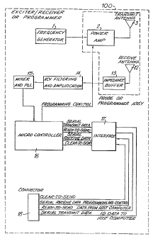
Refersnce is first made to FIGS. 1 and 2 in which block
diagrams of an exciter/receiver (~interrogator~) loo nnd
~rlAnt~hle passive ~LA~ "~ ,An~l,...f~r~) 200 are provided.
Interrogator 100 transmits an exciter signal to ~LAn~ r 200.
The exciter signal is received by ~LA~ ,d~r 200 and powers
tr~nC-pAn~r 200. Once ener~A,ized, LLnn~ oAQr 200 is cnused to
output a data sigral. This data signal includes a prea~ble
portion, ~ , data and identification code. The data slgnal
i5 a PSlC (phase shift lceyed) signal with a 455 I~Iz carrier
frequency. The ~rAn~ ciAn is a rAn~'~n~lA~C, cyclic data stream
containing the ~ r ID and t~ u~-, information. Th s
information is received by interrogator 100 and is ~ Ated,
translated and input to A host ~ I for processing.
As will be AACrr'i h~; in greater detail below"LAr. _~J.~. .f~r
200 ~inr~ C a one time ~iL~r '~ memory 9. PLWL ~~ 100
which is coupled to ~ host computer receives an identification code
that is to be ~ ' intA ~Ln~ nfer 200. Interrogator 100
modulates the amplitude of the excitation signal to co~municate
with tr~n~ 200. When ~,,An~l, ;-~r 200 is in a program ~ode
218g~6
1 5
one time plvyr hl e memory 9 may be ~L~J~L -~; by interrogator
100 .
In an exemplary embodiment, interrogator 100 CommunicateS
with tr~nap~nAer 200 through inductive coupling known in the art
from U S Pate~t No. 4,730,188 rhe interrogation
signal is less than lo ~Iz and more precisely 7109 H2. The return
data stream output by the tr;lncponr~ - i8 output on a higher
frequency carlrier signal of 455 EHz.
A more detailed description of the inYention is now
provided. Description is made of the system in which tr;~ncp~n~
ioo already has been programmed and a user ~aole~~~ed identification
code has been stored in one time PLV~L ~hle memory 9.
Interrogator lO0 includes a frequency generator l which outputs a
7109 Hz signal. A power amp 2 receives the output signal and
causes the signal to flow through the primary coil of a transmit
antenna 3 which generates an excitation field at a frequency of
7109 H2 from exciter 100.
Reference is now made are~-if~c~lly to FIG. 2 in
conn~-c~ n With describing the internal configuration of
~L., ~L~ >~lAor 200. A receive antenna 4 mounted within ~ r
200 receives the exciter signal from interrogator lO0 and inputs
a 7109 Hz signal to a rectifier/regulator 5. P~ fi~r/regulator
5 receives the AC signal from the receive antenna and rectifies the
signal. me unregulated voltage is then regulated to 3 volts to
power the dlgital circuitry c~nt~ined within tr~n~pon~r 200. In
an ~ lAry -ir ' ~ rectifier/req~ or 5 util i7ea Schottky
diodes to reduce the voltage drop. P^~ /regulator 5 limits
the volt~ge to protect the digital electronics. me rectified
signal i8 then passed through a LLe~U~ generator modulator 6 and
input to a data 6 e, - r 7 and manchester encoder and preamble
generator 10.
Data ,4~ r 7 receives as inputs the 7109 Hz signals,
temperature data from a temperature to frequency converter 8 and
the pL~L ~ ID data from one time ~r~L ' 3e memory 9 and
control5 the se<a~n~ in~ of the cyclical transmitted data stream
which includes the preamble, ID data and temperature data. A one
time 1?1~L ~ ' memory g stores the ID data therein. When data
~ 2189~2
sequencer 7 receives the 7109 ~z input signal, it first outputs a
pre2mble enable signal causing manchester encoder and preamble
generator 10 to output a data preamble. It then outputs the ID
data stored in one time prvyL hle memory 9. Data s~quonror 7
sequentially ~ccoCsoa the address to be read from memory 9 through
address bus 202 this causes memory 9 to output the data to data
sequencer 7 which gates the data and outputs the ID data at the
appropriate time to manchester encoder and preamble generator 10.
Reference is now made to FIG. 4 in which a circuit
diagram of data sPq~n~ er 7 is prefiented. Data 5e~1Pnror 7
includes a counter 700 which receives the 7109 Hz signal, divides
by 16 and outputs a 444 Hz signal. One time pLu~L hle memory
9 outputs a program inhibit signal indicative of whether the memory
has been ~L~yL ' by the user with an ID data. The program
inhibit signal has a value of 0 if the memory has already been
lruyL - i and a value of 1 if it has not been P1~L -;~. A first
NAND gate 704 receives the 7109 Hz signal output }~y frequency
generator and modulator 6 as a first input and the inverted program
inhibit signal as a second input. A second NAND gate 706 receives
the 444 Hz clock signal and the program inhibit signal as inputs.
The outputs of both NAND gate 704, 706 are input to a third NAND
gate 708 which gates each of the outputs and produces a clock
signal having a value of either 444 Hz or 7109 Hz as an output.
A binary counter 710 receives the output of NAND gate 708
and utilizes thi~ signal as the internal timing signal. 8inary
counter 710 provides a data clock at its output Ql of 3555 Hz when
a signal o~ 7109 Hz i8 received. Binary counter 710 also
sequentially ~ a~o~a, the ad~.3ses within P~ L hle memory 9
through the address bus at this clock rate.
During the reading of data from memory 9, the accessing
of each memory causes ID data to be output by memory 9. This data
i8 then input to a clock 718 which receives as a clock input the
3555 Hz data clock output by binary counter 710. This is to
synchronize the data being output by memory 9 with the trans~it
se~on~ o as l~L- sL.~Led by the data clock.
A NAND gate 714 and a NAND 716 are provided to gate the
tr~nC~iaairn of the preamble, ID data and temperature data portions
of the cyclical transmitted data stream. NAND gate 714 receives
-
.. 2189~62
7
the output o~ Q8 as one O~ its inputs and the output o~ Q9 as its
other and outputs the preamble enable signal. NAND gate 716
receiveG the inverted output of Q8 and the output of Q9 and outputs
the temperature enable signal so that the two NAND gates will not
enable the tr~ncmiC~cio~ o~ the respectLve data simultaneously.
Additionally, a NAND gate 720 utilizes the preamble enable signal
to gate the temperature data being produced by temperature to
frequency converter 8 so that when the preamble enable is low, the
temperature waveform is blocked.
During the read operation, the program inhibit signal has
a low value, therefore, its inverted signal is high. Because one
input of NAND gate 706 is 0 (the program inhibit value), it wlll
cont i n~ cl y produce a high output. Whereas the inputs Or NAND
gate 704 are a continuously high signal and the oscillating
~aveform signal of the received 7109 Hz signal, the output of NAND
gate 708 will be a 7109 Hz clock signal. Binary counter 710
utilizes this signal producing a data clock of 3555 Hz and a read
out rate of 3555 Hz.
In an exemplary ~ t, if the output of Q9 is low
the preamble data is output and then the program ID data. once the
value of Q9 goes high, the preamble enable goes high allowing the
temperature data to be transmitted through NAND gate 720. During
the time Q9 goes high, the EPROM Or memory 9 is still s~
However, the ID data is not output by the m~n~ h~Gt~r encoder And
preamble generator 10.
To obtain the temperature data portion o~ the output
signal, a chip thermistor 19 i8 provided which outputE~ a resistance
in ,~ 2 to changes in temperature. The resistance is input to
temperature to fL., ~ converter 8 which converts the resistance
to a r.e~uer.-,~ which is input to data se~ r 7~ In an exemplary
_~i l, t~ t LUL~ to rL~ uen~y converter 8 is an RC
oscillator that is controlled by the resistance of thermistor 19.
The frequency of the oscillator increases with t~ I uLæ. The
oscillator has an approximate rreguency of 160 ~z at 36-C. Data
G~ Pnt~t~r 7 gates this frequency and outputs the signal to
manchester encoder and preamble generator 10 at the appropriate
time allowing r-n~ h~Cr encoder and preamble generator 10 to
2189~2
output a cyclically transmitted data 6tream which includes the
preamble, ID data and temperature/frequency data.
Manchester encoder and preamble generator 10 receives the
1109 Hz signal and Le~v-.-ls to the preamble enable, t~ ur=
enable signals, data out and data clock signal produced by data
~e~uanr~r 7. When the preamble enable signal plodu~ed by data
sequencer 7 is high it encodes the data being transmitted by data
sequanrar 7. The 7109 Hz clock is selected as the manchester clock
and the data out signal is always high producing an output twice
the nornal data clock frequency. This allows a sinple means of
detecting the beginning of the cyclical data s~ anre. In a first
stage, the manchester clock is mixed with the ID data to produce
nanchester encoded preamble and ID data signal. In a next step,
when the temperature enable signal is high, the manchester encoder
and preamble generator 10 replaces the mcu~cl~e~Ler encoded ID data
with the temperature data completing one cycle of data
transmission. This data is transmitted at 3555 baud to frequency
generator and modulator 6. By way of example, the preanble, ID
data and t~ ~ILuLe data are pLv-luced in this order. However, as
the entire output signal is c~lnt;nllo~q and cyclical, the
temperature data may be output f irst .
FL~YU~ ;Y generator and modulator 6 receives the data to
be transmitted from manchester anro~in~ and preanble generator 10
as well as the received clock signal of 7109 Hz. F~ ;y
generator and modulator 6 multiplies the input clock signal by 64
to produce a transmit carrier rL.zyu~ y of 455 KHz to output a 455
KHz carrier signal containing the data. This carrier ~ignal is
phase shirt~d by 180- when the transmitted data changes state to
output a phase 6hift keyed signal.
Reference is now made to FIG. 3a and 3b, wherein a
circuit diagram of r~_~u~cy generator and modulator 6 is provided.
The circuit shown in FIG. 3a operates digitally on the received
7109 Hz 6ignal and provides an input to an analog portion of the
circuit shown in FIG. 3b. The freyuency generator and modulator
multiplies the frequency of the received clock (7109 Hz) to produce
a 455 KHz carrier signal by comparing an internal digitally
controlled oscillator with the period of one cycle of the received
clock signal.
2183~62
An analog oscillator is provided having a capacitor 649
which is charged by a combination of voltage sources 630, 634, 638,
642 and 646 having valucs of i, 2i, 4i, 8i and 64i respectively.
The current is input to capacitor 649 to charge. Capacitor 649 is
coupled to inverters 648, 650 arranged in series. The output of
inverter 650 is input to a MOSFET transistor 652 for discharging
capacitor 649. This continuous charge and discharge provides an
oscillator of a certain frequency. The rate of oscillation is
based on the current sources so that the amount of charge stored
in capacitor 649 as a function of the amount of current and then
discharged by transistor 652 causes oscillations within the circuit
producing pulses at about 910 RE~z. In an exemplary
capacitor 649 has a value of 10 pF.
The 910 KHz signal is input to a divide by 256 circuit
which includes NAND gate 610 and two binary counters 608, 612. The
910 E~2 signal is input into binary counter 608 and is also one
input of NAND gate 610. The second input of NAND gate 610 i5 the
divided output Q3 of binary counter 608. The output of NAND gate
610 is input as the clock input of binary counter 612 so that the
output Q3 is a signal having a rL- ~-el~-y of about 3554.68 Hz.
At the same time, the received 7109 ~}z signal is received
by freguency generator and modulator 6 and is inverted by an
inverter 602. The inverted received signal is input to a flip ~lop
604 as the clock input. Flip flop 604 is a divide by 2 so that its
Q output is a signal having a frequency of about 3554 . 5 ~z . This
signal is a~,y~ L~ ous with the 3554.68 signal of the divide by 256
circuit. A NOR gate 618 receives the two signals as does a NAND
gate 616. A comparison is made between the two signals to
determine which occurs first and ad~u~,i are made.
To prevent toggling back and forth between one coming
before the other at NAND gate 616, a delay circuit is provided.
The delay circuit includes the flip flop 606 providing an input to
the flip flop 620. Flip ~lop 606 receives the 910 KHz signal as
the clock input and provides a Q output to flip flop 620 received
at the D input of flip flop 620. Flip flop 620 again clocks this
signal with the 910 KHz pulses of the oscillating clock formed
about capacitor 649. This del~ys the output of flip flop 620 by
at least one cycle of the 910 KHz pulse signal.
2189~62
A pair of NAND gates 624, 626 are provided. The output
Q Of flip flop 604 repre6enting the divided down received signal
having the 3554.5 Hz frequency is input to both NAND gates 624, 626
as is the delay Q output of flip flop 620. However, NAND gate 624
receives the inverted output of the divide by 256 circuit (the
3554 . 68 Hz signal) while NAND 626 receives the actual signal
itself. The outputs of NAND gate 624, 626 control are input to an
updown counter 628. The outputs QA-QD of updown counter 628
control the amount of current rlowing from each current source
through switches 632, 636, 640, 644 respectively to the capacitors
649 .
The relative outputs of NAND gates 624, 626 control
whether the amount of current fed to capacitor 649 should be
increased or decreased thus affecting the frequency of the pulses
produced. This is a delayed function so that no matter which
signal, the divided receive signal or the divided oscillator signal
goes high first it will be delayed before the gates 624, 626 are
able to dptprmi nP whether the count of up down counter 628 should
go up or down. If the output Q of flip flop 604 goes high first,
it is delayed by flip flops 606, 620. If at the same time the
output at Q3 of binary counter 612 is low, the input Or NAND gate
624 would be high while the input of NAND gate 626 would be low.
The output of NAND gate 624 would cause an up pulse at counter 628.
The counting of flip flops 608, 612 are controlled by
flip flop 614 which receives the Q output of flip flop 604 as its
clear. Flip rlOp 614 in turn controls the resetting of flip flop~i
608, 612 and th~reby controls the output of the divide by 256
circuit. Additionally, the clock input of ~lip rlop 614 is the
output o~ AND gat~ 616. If the output Q3 is 1, the Q output of
flip flop 614 goes high causing output Q3 of flip flop 612 to go
low again restarting the whole process. Counting can only occur
when the Q output of flip flop 604 i8 low.
If it is det~ npd by NAND gates 624, 626 that pulse~
are not being output at 910 KHz corrections are made by updown
counter 628. Switches 632, 636, 640, 644 are analog switches which
allow the current from the respective current source 630, 634, 638,
642 to be output to the capacitor 649 to charge it up at a faster
rate thereby increasing the fL-~ ;r of pulses. As the need for
~ 11 2189~
an increased freyuency arises, the number of switches 632, 636 and
the like which will be turned on to allow current to pass to
capacitor 649 increases sequentially until the frequency of the
pU18eS i8 sufficient.
A divide by 2 flip flop 654 receives the 910 }~Iz pulse
as a clock signal and outputs as a Q output a 455 KHz signal. The
455 ~z signal is the carrier freyuency for the data which is
transmitted by trAncpond~r 200. An exclusive OR gate 656 receives
the 455 E~Iz signal and the data to be transmitted in~ in~ the
preamble, ID data and temperature data as a second input. ~he
exclusive OR gate shifts the phase Or the carrier signal by 180-
in response to the data so that a phase shift keyed data output
signal is prvduced by exclusive OR gate 656. This phase shift
keyed signal is then transmitted to interrogator 100 where it is
operated upon.
By multiplying the received clock by 64, a transmit
carrier freyuency of 455 la~z is obtained. By digitally comparing
the period of 64 cycles of the internal digitally controlled
oscillator with the period of one cycle of the received clock, a
very inaccurate freyuency source can be synchronized with a very
accurate r~e.lue~-;y source to produce an accurate carrier freyuency
at a much higher rL~dy.~_..cy without imposing limits on the rreyu~... y
values. As rl1~ o6~7 above, this is A~ d by determin1ng
whether the received clock cycle is shorter or longer than the 64
cycles of the oscillator. Ir the received clock cycle is shorter,
then the oscillator r.., ~ is too low and a up pulse will be
generated output to an updown counter control 1 ing the current
sources to the capacitor. If the received clock cycle i~ longer,
then th~ osci11ator freyuency is too high and a down pulse is
generated and output to the updown counter.
The phase ~hift keyed data is output through
r~ctifi-~r/regu1ator and a transmit antenna 11. A 455 RHz ~ield i~
produced which i9 received by receive antenna 12 of interrogator
100 .
The received signal is input into an; ,-'-n-~ buffer 13
which buffer8 the high i --n~ e of the tuned receive coil rorming
receive antenna 12 80 that the much lower i ---n~ e of the receive
filter does not reduce the received signal -L~ Lh. The 1 --~n--e
218~462
12
ma~ched signal is an input to a receive filtering and amplification
circuit 14. Receive filter amplification circuit 14 filters out
unwanted signals and amplifies the received signal for further
processing .
In an exemplary . --ir--t, receive filtering and
amplification circuit 14 uses a multiple pole ceramic band pass
f ilter with a +/- 15 ~EIz pass bandwidth and 60 dB attenuation in
the stop band to filter out unwanted signals. The signal is then
amplified with a gain of 40 dB. The circuit is shielded and the
power supply are isolated to keep external ele~.~L ^ti~
influences from corrupting the received signal.
The amplified received signals are then input to a mixer
and phase locked loop 15. The mixer receives the received signal
with a 410 KHz signal to produce a base band received signal at 45
RHz. The phase locked loop ~Lolu.:es a positive pulse with every
180- phasQ shift of the received signal. These pulses are then
input to a micro-controller 16 where the received ID data i8
rt~ Lucted and the temperature d~ t frequency forming part
of the output data stream from trAn~ 200 is detected and
analyzed .
Mi~L~ _ul.~roller 16 ~-~c.,.l~.L,u~:Ls the ID data portion of
the received signal and temperature information from the frequency
pulses output by t~. ~t LaLuLa to frequency converter 8. IIicro-
controller 16 outputs data and appropriate protocol signals which
may include a ready to send signal indicating that the data i8
about to be sent, the transmitted data is then sent in serial
fashion to an RS 232 interface 17 which converts the data from
digital levels to RS 232 levels. This converted information iA
then pa~l~ed through a connector 18 to the host computer at which
the data is to be ~cc~ised.
By providing a passive ~,~ h-~ r which contains a chip
thermistor and, a temperature r,- 5~u~n~;y converter, it becomes
possible to monitor the temperature of the animal in which the
LL~ n~ r has been ~ lAntad. T. aLULa is utilized merely by
way of example. Through use of a data s~TI~n~ r as described
above, other system status characteristics, such as l ar
.~_u~a~ light levels or other fluid condition~ may be
continuously monitored and transmitted to a remote host computer.
_ _ _ _ _ _ _ _ _ . _ _ . . . _ _ _ _ _ _ _ _ _ _ _ _ _ _
` 2189~2
13
Additionally, by providing a freyuency multiplier within the
trAnGpon~Pr it becomes possible to use an interrogatiOn signal of
less than 10 ~z, a non-FCC regulated freyuency, making it possible
to increase the power utilized to send this signal thus allowing
increased read distances between the inductively coupled
interrogator and tr~nGpon~Pr. Further, by utilizing a rreyuency
generator and modulator in which an internal digitally controlled
time period i5 compared with one cycle of the received clock and
operated thereon, a very inaccurate freyuency source, the
internally generated oscillator clock, can be synchronized with a
very accurate freyuency source, the received signal, to produce an
accurate freyuency source at a much higher rreyuency which is more
suitable for transmitting the more complex transmit data stream of
the tr In~p--ndPr.
P
Reference is now made specifically to FIGS. 4 and 5 in
which y~ L i nq Or tr~nGp~n~Pr 200 is described. One time
pL~JyL. -hlP memory 9 ls an EPROM which always has its output
enabled. Be~ore it is been p]~ L -', it ic in a program mode
tProgram inhibit is high) as seen from FIG. 4. This causes data
~equPnCpr 7 to operate at an internal clock of 444 Hz. Prior to
pLv~L inq, each address Or one time IJ~O~L hle memory 9 has a
value of 1. The program inhibit signal causes data seq~lencer 7 to
operate at an ~n~PrnAl clock of 444 Hz. This clock causes counter
710 to operate at a slower 444 Hz speed cau6ing the tr~n~ n
of data to occur at the slower speed. Accordingly, when the
carrier signal i~ produced at r~y~ y modulator 6, the PS~ data
rate is lower than that dlccllccPd above when the already p~L - ~
ID code i8 utilized. This is duQ to the slo~er data clock o~ data
B e y - ~ 7 . This lower rat~3 is at 222 band a~ opposed to 3555
baud utilized during normal data transmission.
Generally during ~LOYL ing interrogator 100 receives
this dirferent data rate and recoqn1 ~PG that P10YL ~1 e memory
9 has not been pro~L '. It then scans the ID portion of the
data signal and compares it address for address with the ID number
to be ~ L ~' into tr~n~r~n~lPr 200. If the values for the
addres6 do not co~nc{cle, then the values are changed until the ID
14 21894~2
data that is stored in ~L~LI hle memory 9 ~L~:-.~...ds to that
in the host computer.
More specifically, interrogator 100 in a manner almost
identical to that discussed above with the exception o~ the slower
data rate causes binary counter 710 to increment the address of the
~royL,--,.,uable memory which is presently being ~cc~ssed. Initially
all 128 bits in the EPROM are set at 1. If the value of 1 is not
correct for the presently ~Cc~ccpd address, the host computer
causes mi~:~u c~",LLuller 16 to output a pLuyL~l~ing control signal
to power amp 2. This causes power amp 2 to output a high voltage
signal through transmit antenna 3 to receive antenna 4 of
tr~nCp~n~r 200. This high voltage signal becomes a 12 volt signal
arter processing by rectifier/regulator 5. This ~LO~L ; ng
voltage is input directly through the PROG input of one time
~royL~l~able memory 9 to change the value at the present address
of the EPROM from a 1 to a 0. This process is repeated for each
address of the EPROM. If the value of that address is correct as
1, it is merely scanned, not operated upon and then the binary
counter advances to the next address. As each address is read, the
value of that address is output through the DATA output of one time
~L~)~L hle memory g and is pl.,cessed by data seq~l~n~ c~r 7 as
,q~ cc~lcsed above.
During P~ L ln~ mode, the program inhibit signal is
1. Accordingly, the inputs of NAND gate 706 and NAND gate 704
become switched from the above ~ cll~ed reading mode. The input
of NAND gate 706 is 1 and the 444 Hz signal 80 that the output of
NAND gate 706 is a waveform having a rL-,~u~ of 444 Hz.
Additionally, the inputs of NAND gate 704 are now 0 and a waveform
so that the output of NAND gate 704 will always be 1. Accordingly,
the clock used by binary counter 710 during the pr~ ing mode
is 444 Hz which results in a data clock of 222 Hz. The operation
of the enable gates and the temperature gates are identical as that
described above.
When the last address of the one time ~L~r -hle memory
9 is IJL-~L ~'~ the value is changed from 1 to 0. This causes the
program inhibit signal which is output to change the internal clock
of data sDTl~n~r 7 from the 444 Hz rate to the 7109 Hz rate.
Accordingly, during the next interrogation by interrogator 100,
'` '` 218g~2
interrogator 100 d~tPrminp~c that it should not program tr~ncr~n~l~r
200 based upon this new received PSK data rate.
To produce the PLUYL ;ng control 6ignal, power amp 2
is provided with a P channel power MOSFET causing 24 volts to be
applied to the exciter primary. This causes a much more powerful
excitation field to be generated. It is this high excitation field
which causes the bit presently being ar~c~c-ed within tr~ r
200 to be yLu~r -' to 0. On the receiving end,
rectifier/regulator 5 is provided with a Zener diode to limit the
plc,y~ ,ing voltage to the 12 volts diccllccs~ above.
By providing a pLUyL -hle memory which outputs an
inhibit signal once each of its addresses has been pr U~L ~ ' and
a data 6ey--l~n~-~r having an internal data clock which functions at
a different rate during pruu~L in~ and during reading, a one time
pLuuL~lllLll~able memory is provided which allows a PIUYL using the
interrogator t--n~l, 7~r system of the present invention to select
his own non-erasable identification codes for the animal being
monitored after manufacture of the t-~ ar. Additionally, by
utLlizing a slower freyuency signal during YLUU,L in T then during
receiving, the efficiency of both programming and transmitting of
information is DnhAn~ ~d.
Reference is now made to FIGS. 6-9 in which a tr~-~p-- '~r
200 cul.DLLu ;Led in accordance with one ~mhodi- t of the invention
is proYided. TrAncpond~ 200 1 n~ 5 a substr~te 25 .
Rectifier/regulator 5 is mounted on substrate 25 along with a chip
thermistor 19. A chip 20 housing the structures of rL.lu~
generator and modulator 6, data sey .-~ ~ t 7, ~ LUL~ to
r.c~uen~ ~ converter 8, one time ~LU~L hle memory 9 and
manchester encoder and preamble generator 10 is also supported upon
~ubDLLc~te 25. Rectifier/regulator 5, chip 20 and chip ~h~rm~tor
19 are electrically coupled to each other by connecting traces 27
deposited on substrate 25.
Receive and transmit antennas 4, 11 are formed about a
~errite rod 21. Transmit antenna 11 is formed by wrapping a coil
31 about ferrite rod 21. Receive antenna 4 is ~ormed by a coil 3~
wound about ferrite rod 21. Coils 31, 34 are coupled to
rectifier/regulator 5 through bonding pad 24.
16 218946~
In an exemplary embodiment, trAnCp~n~lDr 200 is
Pn Ir5~l1ated in a glass capsule 28. The capsule is .500 inches to
.750 inches long and has a diameter of .080 inches to .100 inches.
The glass capsule may either be coated with a protective epoxy,
replaced entirely with a protective epoxy or treated to prevent
migration in animals.
Interrogator 100 may be housed in two distinct portions
for ease of use. Power amp 2, imrP~l~nrp buffer 13, transmit
antenna 3 and receive antenna 12 may be housed in a probe assembly
as known from U.S. Patent No. 4,526,177. The ,. ~nin~ structure
of exciter 100 may be housed in a separate housing. Such
differentiation of structure reduces any interference from micro-
controller 16, r~C~Uell~ y generator 1 or the host computer to
either the transmit antenna 3 or receive antenna 12.
By forming the frequency generator and modulator, data
sequencer, memory, temperature to frequency converter, and
manchester encoder and preamble generator on a 6ingle chip,
efficiencies in size and cost may be obtained. By forming the
entire tr:~nF:p~nrlP~ less than .750 inches long and with a tli: - Pr
of .10 inches or less, the entire assembly becomes implantable.
It will thus be seen that the ob~ects set forth above,
and those made apparent from the preceding description are
efficiently attained and, since certain changes may be made in the
above ~ ullD~Lu-;~iOn without departing from the spirit and scope of
the invention, it is intended that all matter ~ont:~inPcl in the
above description or shown in the ~c ying drawlngs shail be
interpr~ted a~ illustrative and not in a limiting sense.
It is also to be understood that the following claims are
intended to cover all of the generic and specific features of the
invention herein described and all statements of the Dscope of the
invention which, as a matter of language, might be said to fall
th~r~