Note: Descriptions are shown in the official language in which they were submitted.
T T I~f'TT fl~TTC CrT f~TTTT AMENDED SHE.T
This invention relates to an electronlc circuit. ~ore particularly,
although not exclusively, it relates to an electronic ci-cuit for
5 d~ rm;nAt;~n of distances between refGrence and data pointq
E12ctronic circlits for rl~Armin;n~ Euclidean distances are known in the
prior art. Such a circuit incorporates a stored quantity c~rresponding
to a reference point and accepts as input a signal representing a data
iO point. It produc~s a measuro of the distance between the input signal
and the stored quantity. Such circuits are useful in Rrrl;~R~;~nq in
which calculations of Euclidean distance would consume a substantlal
amount of computing capacity. In viqual and speech recognition,
together with o~her iorms of pattern rq-ot~n;t;~-n, i~ is necessary to
lS detormine Eucl_dean distance between large numbers of input data points
and each point in a large database of reerence points.
~TS paten~ 3 864 558 discloges a par oE fie`ld effect transist3rs (FET91
with ~ memories arranged to determine the square of the
20 distance between two poi::lts represented by voltages. The FET memories
are IJ~, 1 by getting the threshold voltage. When tha, rqn~:i ct~lrq
are operated in saturation, the output current is dependent on the
square of tha difference between this prn, ' voltage and an applied
ga~e voltage and hence is representative of the dista~ce recu~red. A p-
75 channel and an n-channel FET are connected sourcc to drain in
antiparall~l. The two gates are connected together such that only one
FE;T conducts under an applied gate bias, the particular FET produc~ng
the distance reprl~q~ntAtimn being dependent on whether the applied gate
voltage 19 greater or less then the stored threshold voltage. In this
30 way an anal~gue for the square of the difference between a first
magnitude and a second magnitude is produced, regardless of t.~le polarity
of this difference. ~Jsing ~ G;milAr-type FETs however makes it
difficult to match device characteristics. Differing carrier mobilities
and other physic~l characteristics mean that e~ctre-me diff:culty i8 met
35 i~ mak:ng allowance for the efi'ects of device mismatch.
In ~A reural Neteork Capable oi Forming Associa~ions by 3xample~, ~eural
~etworks Vol. ~ pages 3~s-403, }~89, ~artstqin and ~och disc'ose a
2 ~ 1 8 9 ~ 4 8 ,;~j~,eilL~ t.
similar aLL~Ly_...~ of FETs. A t~ro-trelnsis~or clr~uit i_ used in a
neural network to represent the ~ f~ .lr~ bet-Neen a voltage Lrput and a
stored or learned value . T~o me~al oxide ~mi rrnol11rrr_ field effect
transistors (MOSFETs), a p-channel and an n-chanrel MOSFET are this time
S connected in parallel in a symmetric ~LLCIILy~ t in order to ~ obta~ a
symmetric output f mction for the neural network. ~7artstein and r~och
are not however concern~d with Euclidean distance ~t~rm1n~r1rn, but
instead output function symmetry. This symmet~~lr rerluires close~matching
of the characteristics of the p-channel and n-channel devlces and if it
10 is not achieved, the output of the circuit is not suitable for E 1r~ 1.1..=~
distance ~l~rOrm;.,qt;r~ j
In ~PLIJYL hl r Analogue VLSI for Radial 3asis Functlon NetaorksN,
~1i.rtrr~1re Letters 2~(18), pages 1663-1655, Septiimber 1993, Churcher et
15 al. describe a I ..."q~ ,.".1~,~ a~r~ amplifier ~Nhick produces an output
current proportional to the sguare of the difference (distance) between
an input voltage and a stored ~oltage msl1~t=in~ by a capacitor. The
amplifier produces an approximation to the 5r.~uare of the F~lrl ;~PN~
distarce between the input and stored voltages. It is not suitable for
20 ~rr1;rqr1r~N such as pattern r~rr,r,nit;r" requiring a large number of
distance measuring circuits. It incorporatar a number of transistors,
two of which are rr"e;~rahly wider than the rest, which gives rise to
difficulty as regards format:on of large arrays. The transis.ors also
suffer from high power consumptLon when operatlng Ln thair ==r1.ri~t1
25 region
A similar disadvantage is apparent in the c rcuit described in ACMOS
Selfbiased ~11rl iol~=r Distance Computing Circuit with Eigh Dynamic
RangeN, Electronics Letters N7~L (4) page 352, 1992. O.Landolt, E Vittoz
30 and P.~eim describe a devicQ which outputs a repr e-7nt~t1rn of the
function
Iouc=~
for the n-~11m~q1r~=1 vector oi~ bi-dir~ctiona: currents I, .. l=-
iIowever, to calculate Euclidean distance, these current3 cannot be
35 representative of vector, ~ntq ln themse1 ves but of the r1 ~f~ nr.
bet~e~n -rector ~ ~ q. Such clr-ents car be sererated using a
~! 3 2 1 8 9 6 4 8 AMENDEO ~
slmpl~ switch~d-curren~ memorf ce:!l, but thls ~ l requlre a minimum of
ou~ e~tra ~ransistors per dimension. Thus the complete circui~
r~nn~Ainins both the square-law distance r=lr.l~At;l-n and the current
memories is not sllffi n; ~ntly compact for practicable incorporation i~to
lar~e ar-ays.
A two-tranqistor cell has been designed by Castro and Park IUS
.} 999 s251 . It employs two floatiny gate transistors to implement an
exclusive-or operation botween two digital patt2r_s. Cells are cascaded
togetker to calculate a E~amming distance between an input vector and a
stored -eference vector. The cell requi-es a separa~e high-gain
inv~r~e~ to complement the input vector, restrict:ng the cell to :digitaI
operation .
In "An Analog ~il,SI Chip for Radial 3asis Func~ionsR, Advances ir~Neural
~nC^rmation P-ocessi~g Systems ~, Morgan Kaufma~ 1993, Anderson et al.
disclose a distance r?Pt~in~t-mn ch~p employing an inverter with an
adjustaole threshold. The threshold is set usinS a floatirg gate device
suc~ as 'hat descrlbed by S.M.Sze in UDhysics of 3~mi,~n~il.,rr,r Devices",
Wiley 2nd Edition lg81, page }96. This device is u~u~ -1 using a
r,-ml~lnAri~n of non-avalanche injection and t-lnn,.lling
mke ~nderson e~ al. circult has a ma~or di3advantage that ts output
does not correspond to a tr~le 3uc'~ ~ dean dis~ance or square ot a
3uc_idean distance. Instead, the output cur~ent approximates to a
quadratic unction only in the region of a pealc current value. ~he
approxim.ation is only valid over a shcrt range cf input voltages, less
than 0.35V in the ;mrl~ A~imn of Arlderson et a_ _ -
30 A low-power differenc~ r~ mllArlns neural 1etwork developed
M,A.:~oller, S.M.Tam and A.E.Kramer is descr~oed :n UK Patent Application
2 257 172. This net-~ork m~llllAtl~q the absolut_ ~City 310ck 31stance"
betAleen an input voltage _nd a _tored -eference ~oint, referred to as a
~elgh~. The A,eight is stored by meanS of a float_ng gate charge "rhich
35 ~Pt~rminl~q the threshold voltage o the device. ~n applied input (data)
~ol~age causes charges _o develop "r~ th n the char.r.el regiors of selected
MûSF~Ts, the magnitude ot this charge being pro~ort_onal to the
d: _~r~nce bet.~e-rl tie ap~l-ed dat~ -/clta~e anc tre thresholl -rolt=ge.
4 2 1 8 9 6 4 8 ~ ,;~ !. ~
rhe MOSF~Ts of the same column are then di:acharged ard the associated..
charge pac.'cet3 of a column oi ~OSFETs are summed. This summed charge
thus represents the City ~310ck distarce for that col~mr.
5 T.~e Clt~f BLock ~Alr--lAtion does .not havc as many or as useful
appllcations as the Euclidean distance calculation. City Bloc3c, also
known as Manhattan, di3tances are sensitive to a change of axes and so
AC ,' irnq have ~o be made regarding the nature of tke data in order
that appropriate axes are se1 ected. Euclidean distance is far mor~
10 useful in practicaL R~rlnl;r~tlrnc because its inherent s-fmmetry renders
it ;n,1~,nrn i:-nt of axes or;,~ntAtinn It thus offers a more robust and
portable technique for distance rAlr~lAtinn Further disadvantages
arlRsa from operating in the charge domain in pref~rence to the current
domaln. The accuracy ~lth ~hich charge is s~ored on floating gate
15 devices i3 senerally an ~n~l~tor-ninAhl~ quantity; the re~erence level may
therefore carr~ an inherent uncertairty. Moreover, ~ven identicall~f
prod~ced MOSFET3 exhibit ir~ter-device -~ariations leading to differing
threshold voltages.
20 Each of che foregoing prlor ar~ techniques suffsrs ~rom at least one of
the following disadvantages- unadapted to Euclidean distance
calculatlon, 1 arge chip area rerluirement3, high ?ower consumption and
res-~iction to a shor~ rarge of input voltar~es or to digital
lmplr~n~"tAt;r" only. There lS a 2erceived need for a ci~cuit~ which
75 admits of compact cons~uction, is operative over a useful range of
input -~oltages, calcula=es the mure useful 5uclidean distance and i5
suitable for analogue ~pl~ ntRr;on~ There is also a trend towards
developing lower-power devices suitable for dis~anc~ ~Al~ At;onq -
~portable Aystems.
It is an object of the invention to provide an alterr~Ative form of
elec~ronic cir~ui~ suitable ~or use in distance ~rt~_ninAt;on such as
the Euclidean norm
35 The present invention pr-vides an electronic circuit comprising
(i~ a yL;,y. hl e c'nresrold trarsijtor palr of like charnel
c^nductivity tfpe ~qqor Rri- i with a common output, ar~d
6 4 8 ~ a~ ~-
( li~ means ior applying complamentar~,~ analogue Lnput voitages to re.e =
transistor pair =~
S characterised in t~at the circuit also includes
ULU ~L n~ mean_ for LyL~, n~ the threshold voltages of the
transistor pair to provide for output current to be a quadratic or
exponential function of the di~erence between a ~ILU~ 'I reference
10 and sllhc~nlPn~ transistor pair input data voltages in ~ 1 ~m,nt~ry
analogue ~orm.
The invention has the advantage th~t it provides a measure o distance
bet~..reen data and re~erence points represent2d as input and referonce
15 voltages, and it i9 capable of construction in compact form with low
power requirements. It is well auited to replication to form an array
of circuits ~or performing multiple and multidimensional distance
-minArimrq.
20 The transistor pair o~ the invention ma~,r be arranged for sub-threshold
operation . The ~ULU~ ' ng means may lnclude meens for applying
yLUy "~g vol~ages to the transistor pair such that the supply o~ the
re~erence voltage, in conjunction ~ith tlle supply of the ~LUyL n~
voltages, and the subsequent supply of the in3ut data voltage causes a
2s :signal at the cor.~mon output which is an ~rrmn,~nri~l Function of the
diLference bet~een the reference and data voltages.
This ~im~.n~ of the invention is advantageous because of i~s
suitability ~or low voltage applications.
The input ~oltages may be in the range OV to 3 . 3V, or, preferably OV to
1. SV, thereby rendering the circuit capable o~ oper~tion with a
conventional digital logic power supply o~ 3 . 3V or a 1. sV battery power
supply respectively.
The circuit of the invention preferably includes a diode-connected loadtransistor having a drai~ connected to the common output and arranged to
produce an output voltage which is a 'unction 3f the dir~rence bet-aeen
6 21~
AMENDED SHE~ -
the reference voltage and the input data vo1 tage . The lo~d transistor
may also be arranged Sor sub-threshold operation. Th;s ~eature is
capable of further l1miting power consumption.
S The clrcui~ of tlle invention may be incorporated into an array of like electronic circuits each having a respective transistor pair, at least
some of the transistor pairs havlng outputs connected to a common
summing means and thereafter to a diode-connect~d load transistor
arranged for sub-threshold operation such that the load transi3tor
10 output voltage i3 3ub3tantially proportional to the natural logarithm of
the sum of the output current3 from the 3elected tran3istor pairs. Such
an array provides the capabllity for perSorming multiple and
multidimensional distance i~rmin~ inn=
15 In another aspect, the invention provides an 1~l r~ron1- ~ ircuit
characterlsed in that the ~LU~ L 'ng means includes means for appl-,~ing
~L'~yL ~nrJ voltages of 3u~ficient magnitude to operate the tran3istor
pair in their 3aturation region3 and to provide for them to cxhibit an
outpu~ current proportional to a quadratic function of the dlf ference
20 between a reference voltage and an input data voltage. In thi3 aspect,
the invention provides a measure of the Srluare of the Euclidean di3tanc~_
between a reference point and a data point repre3ented by circuit
.~o l tage3 .
2s The invention prefe~ably al30 include3 mean3 for appl-"ing respective
input voltages to the t~--ansistor pair simultaneously, one input voltage
beiing the complement of the othe~. This pair 'ormation enables '.he
circuit to give a 5uclidean distarcc output regardless o~ whether the
reference voltage is lower or higher than the data voltage.
The programmable transistor pair may b~ metal oxide field effect
transistors each of the kind incorporating a control gate and a floating
gate and further rh~r~rt~ in that the ~ L 'nr~ means comprises a
means 'or storing charge on the fioating gatas.
The circuit preferably include~ means for deri ~ing square roots
connected to the common output, ~hicn in a preferred embodiment is a
diode-cornec~ed '~ oad transis~or having a drain cor,nected to the common
7 21 89648
F,~i2i_~ - -7'
out?ut ard arranged to procluce an out?ut voltage substantia' l~f
proportionaL to the dierence between the reference and data voltages
This lends itsel to incorporation into an array of like electronic
circults each having a respective tranaistor pair, at least some o the
s transistor pairs having outputs connected to a common summing meana ana
thereafter to a diode-connected load transistor such that the load
transistor output voltage is substantially propor'ional to the sauare
roo~ o the sum of the output currents from the selected transistor
pairs. rhis enables t.he Euclidean distance bet-~een multi~ nn~n~ data
L0 and referer,ce v~ctors to be output as a representative voltage at the
load transistor.
In a furrher aspect, the invention may also include resetting means orper:odically resetting the ~L~ei hl.= t~ nni~r~r pair for the purposes
15 oi :ryL-I~ ' ng -~-ith a dif eront value oi reerence -~oltage, In one
.ml.r~lim~nt, the resetting means may include respective rnn~ rting means
corr,ected to the fLoating gates and acti~a~able to conduct ~rhen ecposed
to ultra-violet light, ultra-violet window means arranged over the
rnn ill-tinrJ means, and means for i711.minA~inrJ the rnnrillrrlnr~ means witb
20 ultra-vlol~t radiation, Thia resetting technique is usei'ul or
ins~ances in which the reerence voltages rarely change, and for
ini- - a~ nn to remove unwanted charge ~rom the circuit I3l a second
embodiment, the resetting means may include fi~st and second reset
translstors arranged to 5upply YL"'i nrJ voltages to the floating
gates, The reset transistors may be o~mr~nl 1 ahl - by a reset voltage to ~ =
provlde for:
(1) application of yL'_l~L nr ~oltages to the floeLting gates, and
(ii) isolation of the 10ati~g gates
This resetting techniaue ls advantageous t~ applications in which the
posi.ions of refer-nce points are reauired to be changed electronically,
It also provides a means of Y~'''i nrJ the r~erence voltages with
grea~er accuracy and repeatability
In a i arrher aspect of the invention, each trar.sist~r of the translstor
pair has a current output connect~d to respective switching means, the
3witching means ii connected to '.hreshold ~yL~,y ng- means ard 'o
current summing, and the switching means i3 operative to s-~iec~ the::
transistor output cur--ent '~om the th~eskold i~LvyL ng means to the
8 2 1 ~ 9 ~ 4 ~ AMEN~E3 SHE~T
curranc summing means in response to a pr~l=t~rm~noi circuit condition
This provides the capability of settins the reference point
r-pr~cAnrArirn stored in each transist~r by reference to that
transistor~ s output source-drain current prior to performirlg the cir~uit
5 calculations . This provides for individual yLU~L ' n~ of each
.ran~3istor to compensate for variation in device characteristics and
enabl~s the reference. voltage to be yLu~ ' to a high degree of
accuracy .
10 The circuit is preferential_y arranged such that the transistor pair
comprises floatiL~g gate transistors, and the switching means comprises a --
second transistor pair of unlike-channel transistors An in~ecting
means may also be arranged to apply a ULUyL n~ voltage of ,c~l~ff;mion~
magnitude to a~itablish charge injection onto .the floating ga.es arld
t~ereby to enable variation of transistor current output. This feature :_
provides a straightfor~ard r~Al;=At;-m of a mechanism for varying each
~ransistor~ g output curr~nt for the purposes of plU~ n~ as described
above. The circuit may additionally be arranged such that the threshoid
yLu~L n~ means is connected to a data ~'nput line and arranged t~
21~ switch a voltase applied to the data input llne to a value of sllff;ril~rlr
magnitude to prevent charge in~ection onto the floati~g gates in
response to ~rrA; ' ot a pr~ rmin~ current ~.his aL~L~ ._LL is
capable of providirlg a mechanism by ~hich drain-source current variat~on
lS halt-d when a desired -ralue is reached. This value is= accordi~1y
~s representative of the reference point used Ln subsequent circuit
calculations .
Each of rhe a~orl-m~nti~n~ .mrrmni~ circuits may be incorporatad into
an ar~ ay of like circuits This provides for the determination oZ
30 multiple ana mul';~iim~n~lmnAl distances
An array of electronic ci_--uits of the invention may be characterised ~ n
that each transistor of -very rrAn.; =r~r pair has a current output
connected to switch_L~g means, the switching means ls connected to
35 threshold yL~, 'n~ mean6 and to current summing ,meanS, the switching
means lS operative to s~vitch the ~ransistor outpu~ current f-om the
~hresho'~ 1 ~LU~ ' n~ means to the current r .~mmi~g mears n response to
at~ainment o~ a ~r~ r~ circu~ t condition ~nd aach -lrcuit ~ s
a l 21 89648
connected to a pair of data input lines associat2d with a column of the
array and to a threshold yL~ L n.^j line and a switching activation
line both assoclated with a row of the array. ~his feature provides the
capability for each transistor ln an array of circuits to be ~JLU~. '
individually to a desired level of source-drain current prior~ to the
array performlng a multidimensional calculatlon.
In an alternative aspect the invention may comprise an array of
electronic circuits, each circuit incorporating a pair of yL~ hle
thr~shold transistors, characterised in that the array i~ncludes:
(i) a respective yL~ n~ means for altering the threshold of
each transistor to provide for indl-f:dual ~L~ . r.^j of each
transistor with a reference voltage, the yL~J~L 'n~^; means being
responsive to output current of said transistor;
(li) iAn-put means for applying input voltages to the transistars in
each pair simultaneously, one of the input voltages to each
transiAtor of a pair being th~ comploment of the input voltage
to the other transistor of that pair;
(iii) summing means for -~dding the output currents of the transistors;
(i7) a respective DWitcLi-lg means connect~d to receive output current
^5 from each transistor ~and operative to switch the transistor
output current from the y~ L 'nj means to the summing means
in response to AtO=i ' of a predet~rmined circuit condition.
In this aspect the invention is capable ol multidimensional distance
calculation with a ref~rence point which is _a.,able of being accarately
stored by virtue of an addressable feedback mechai^ism. Such an
individual feedback ~-^~h~n~ renders the c~-cuit capable of reducing
the ef =ect of inter-device variation in transistor characteristics .
~hi, aspect of the invention may also inc'ude operating means for
yL~ 'n~^j each transistor to operate either above or below threshold
and to produce an output current whlch lS a cuadratic or ,fn^n^nri,~l
function of the difference b~weon the ref~nce vol~age and an input
a . 2 ~ 1 8 9 6 4 ~
AMENDED SnEiT
~ata voltage . This provides the advantage of flexibi ~ ity. The same
circuit is adap~able to be used both in Euclidean distance ~,~trrmi~At;~n
and in lts sub- threshold region .
S The array may compri5e ,~ -trnn; ~ circuits connected to form rowg and
columns, tke circuits in each column having inputs connected to a
respective pair of data input lines, and each row incorporating a
respective ~JLUy.L ng lin~ connected to the LULUyL~ 'n~ means of
circuits therein and a respective switching activation line connected to
10 the switching means of circuits there1n. It may also include an
injecting means arranged to ~pply a voltage to the ,UL~yL n~ line of
~l~ff;~ nt magnitude to establish charge injection onto the floati~ng
gates of all transistors in a row The threshold ,ULUyL n~ means may
be arranged to switch the voltage applied to the data input line to a
S value of sufficient magnitude to prevent charge injection onto the
floating gates of all transistors in a column in response to i~tt~i t
of a predetermined circuit condition. Th s enables individual
IJLU~L ns of transistors. This provides the array with th~ advantage
of increased operating flexibility. Each transistor of the array is
20 individually addressa~le and ULU~ hl ~ in this manner, prlor to the
array being arranged to perform a mult;~i;m~"=;n~nAl distance calculation.
In an alternative aspect, the invention provides a method for
determining a distanc~ bet~Areen two points represented by analogue
2s voltages, and comprising the steps of:-
(a) providing a circuit incorporatirlg two ~JLU~L hle thresholdvoltage t~Rn~; ~t~r~ associated with a common current output,
(b) arranging the transis~ors to provlde for their output current t~
be a quadratic or P~mn,~rt;Al function of the difference between
a ULUy ' reference voltage and subseauent transistor ir.put
data voltages in ~ ntAry form,
(c) pLUy 'n~ the transistors with stored reference voltages, one
such -roltage being the complement of the other,
8.3 ~ 1 ~q 6 4 ~ t~ ,n~t~
(d~ applyiny analogue i.~put data voltages to the transistors, on~
such voltage belng tne 1 ~m~n~ of the other .
This method of the invention provides the advantage that it is suited to
S low-power impl,~ n~t;m"q of both Euclidean distance r~ n~ and
sub-threshold applications reauiring fa6ter~ processing speeds than are
achi_vable by computer. Additionally it is realisable both in
individual circuit and array constructions.
10 Another aspect of the invention provides a method of Le:~JLU~L 'r~
circuit arranged ~or the calculation of a function of the difference
between t~o voltages, the circuit comprising a pair of ~LuyL. hle
transi3tors, each transistor incorporating a respective control gate and
a respective floating gate characterised in that the method comprises
the steps of: =
(a) applying ~L~JyL n~ voltages to switching means connected to
respective floatins gates of the transistor pair,
(b) applying a reset voltage to the switc~ling means whereby the
L~L(JyL ng voltages are communicated to the f'oating gates,
(c) applying a r~ference voltage in complementar~ analogue form t~
the control gates of the transistor pair,
(d) removing the reset voltage from the switching means and thereby
electrically isolating the floating gates, and
(e) removing the reference voltage irom the control gates.
WO 95130963 1~~ /41
9 2 l 8 ~ 6 4 8
In order that the invention might be more fully understood an: ' ';
thereof will now be described with reference to the ~ ~ Jing drawings
in which:
Pigure l is a schematic diagram of a circuit of the invention;
Figure 2 is a graph of drain-source current against input voltage
for the circuit of Figure l;
Figure 3 is a graph of output voltage against input voltage for the
circuit of Figure l;
Figure 4 is a graph of output current against input voltage for sub-
threshold operation of the circuit of Figure l;
Figure 5 is a schematic diagram of a circuit of the invention
adapted for refreshable ~.u~, n~;
Figure 6 is a schematic diagram of an array of circuits illustrating
use of feedback in LlL~.)gL_ ng;
Figures 7, 8 and 9 are graphs illustrating progress in ~-o
the circuit of Figure 6; and
Figure lO is a schematic diagram of a further ' '' of the
invention designed to employ feedback in ~ n~.
SUESTITUTE SHEET (RULE 26)
WO 9S/30963 r.~ /41
8'~ 2189648
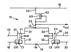
~eferring to Figure 1, there is shown an electronic circuit of the
inTention indicated generally by 10. The circuit 10 incorporates first
and second metal-o~ide sPm;rn~ rtor field effect trsnsistors (MOSFETs) Ml
and M2. The MOSFETs Ml and M2 are floating gate devices, generally as
5 outlined by 5 M Sze in "Physics of SPm~rr~ rtor Devicesn, 2nd Ed Wiley
1981, page 496. MOSFET Ml has a floating gate Fl and a control gate Gl,
and likewise MOSFET M2 has floating and control gates F2 and G2. In IEEE
~lectron Device Letters, Vol.12 No 3, March 1991, Thomsen and 3rooke have
estimated that a floating gate in a silicon MOSFET would lose charge at
10 the rate of 0.1~ in 26 years. Data represented by charge on the floating
gates Fl and F2 is therefore e~cpected to persist.
The MOSFETs Ml and M2 are parallel NMOS transistors which are used to
deter_ine the distance between a data point and a reference point. The
15 data point is represented by input signals consisting of a voltage and its
, the8e being applied to the control gates Gl and G2
respectively. The reference point is represented by charges stored on the
floating gates Fl and F2. The MOSFETs Ml and M2 have respective drains Dl
and D2 connected together at a co=on drain node 12. They also have
20 respective sources Sl and 52 connected together and to earth at a common
source node 14.
A third MOSFET M3, a conventional PMOS device, has a drain D3 connected to
the common drain node 12 and to an control gate G3. It therefore
ZS constitutes a diode-connected load for both MOSFETs Ml and M2 connected in
parallel. It has a source 53 connected to a power supply line 16 voltage
VDD which is positive with respect to earth at the co_mon source node 14.
The floating gates Fl and F2 have coupling capacitors Cl and C2 connected
to respective reference input lines 18 and 20. The lines 18 and 20 are
30 arranged to provide a voltage Vl,.~, to respective capacitors Cl and C2 and
thence to floating gates Fl and F2.
SUBSTITUTE SHEET (RULE 26)
WO 95/30963 P~1.~..,,5.~ 741
? ~, j 11 2 ~ 8 ~ ~ 4 ~
The circuit 10 has a W opaque coating (not shown) through which sre
formed ultra-violet (W) transparent windows W1 and W2 located over
floating gate/capacitor combinations FllC1 and F2/C2 respectively. The
windows Wl and W2 facilitate W illur~ination of the floating gate Fl and
5 capacitor Cl in combination and floating gate F2 and capacitor C2 in
~ nAtinT~ respectively. Data input lines 22 and 24 are connected to
respective control gates Gl and G2. Data input line 22 is arranged to
provide a voltage Vd.t. to control gate Gl, and data input line 24 is
arranged to provide a voltage equal to (VDD - Vd~) to control gate G2.
10 Vd u, cuL.t~,uu..~s to the voltage of a data point and (VDD - Vd~) to its
11 t . The value Vd~ is in the range 0 to VDD. The ~- . ?
voltage may be generated by a conventional differential amplifier arranged
to subtract Vd"~. from VDD with unity gain. A suitable amplifier is shown
at page 99 of P. Horowitz and ~. Eill, Cambridge University Press, 1980,
lS ISBN 0521 23151 5.
The operation of the electronic circuit 10 will now be described in
general terms, a theoretical analysis being given later. The objective is
to determine the Euclidean distance d between a data point and a set
20 reference point. The MOSFET floating gates Fl and F2 have the function of
analogue memory devices to which electric charge is injected and stored.
The stored charge COLLt:~lJUIIdS to a predetermined reference point.
Charge is introduced on to the floating gates Fl and F2 by a W-enabled
25 conduction process. The circuit 10 is ;11 'n~t~d with W radiation which
passes through the windows Wl and W2 only. This renders the capacitors
Cl and C2 conducting; ie they develop leakage current because of W-
activated conduction in their dielectric material. The voltages on the
reference input lines 18 and 20 consequently become applied to the
30 floating gates F1 and F2 via the now r^n~ rt;rlE capacitors C1 and C2
respectively. The process is described in more detail by D A 3~:erns et al.
in CMOS W-Writable Non-Volatile Analog Storage~: 'Advanced Research in
VLSI: Proceedings of Santa Cruz Conference 1991, Santa Cruz CA, March 25-
29 1991', page 245.
SllBSTITUTE SHEET (RULE 26)
W095/30963 ~ 9 ~ 4l ~
The MOSFETs Ml and M2 are l -u~-_ ' as follows . A voltage Vr,~ch i9
applied to reference input lines 18 and 20. It is of sufficient
magnitude to establish the channel surface potential of MOSFETs Ml and M2
at the 'turn-on' voltage (threshold voltage Ve) at which strong inversion
5 occurs. Strong inversion is defined by S2e (see reference above~ at page
373. The eYact value chosen for Vr,t,~ is not critical so long as it is a
little above Ve in the present ; ~ of the invention. Simultaneously
with application of Vr,,rc~, a voltage Vr~e and its r .1 t (VDD - Vr,e) are
applied to the data input lines 22 and 24 respectively, and the circuit lO
lO is illu~inated with W radiation. This n~;nn of applied voltages
results in a charge c~ s~ lding to the position of a reference point y
being stored on floating gates Fl and F2. The theoretical basis for this
is described in detail later.
15 The W illumination is nrw switched off, and the voltages Vr~tC~ Vref and
(VDD ~ Vr~ are removed from lines 18120, 22 and 24 respectively.
The theoretical basis for the invention is as follows. Generally for anNMOS MOSFET with gate-source voltage V~;, and threshold voltage Vt a
20 conducting channel between source and drain is formed when Vg, is greater
than Vt. When the voltage bet~een the source and drain, Vd" is greater
than (V~ Vt) the MOSFET operates in its saturation region, and its
drain- source current Id, is substantially independent of Vd, -
25 For a MOSFET in saturation, the equation for the drain-source current Id,
i8 as followsî-
Id, = ~ ~V,~, - Ve)2 (1)
30 where ~ is a proportionality constant given by:-
CO" ( 2 )
SUBSTITUTE SHEET (RULE 26)
WO gS/30963 ~ ; i S 9 6 4 8 r~ t 741
In equation (2~, L is the length of the conduction channel between sourceand drain, W is the width of the conduction channel, ,L is the charge
carrier mobility and Ce" is the capacitance of oxide between the MOSFET
gate and associated conduction charnel.
Ignoring constants, equation (l) has the same form as the equation for the
Euclidean distance d between two points x and y:
dZ, (y _
Comparison of equations (l) and (3) indicates that MOSFET drain-source
current Id, provides a measure of the square of the Euclidean distance d
between two points x and y represented by gate-source voltage V8, and
15 threshold voltage Vt respectively. E~owever, Ve is a fixed quantity for any
individual MOSFET, and equation (l) does not enable use of a range of
values of both x and y.
In order to use the circuit lO for determining the Euclidean distance in
20 accordance with the invention, it is necesssry to provide for a range of
values of both x and y to be accor~modated. To achieve this, the circuit
lO is first IJLUë,L ' with the voltages Vr,,tch, Vre~ and (VDD - VrQ~) by W
illumination as described earlier. A voltage Vt e., representing the
position of a data point, is then input on line 22 to control gate Gl, and
25 its, .1 - (VDD - Vd~e~) is input on line 24 to control gate G2.
At this point the potential Vf8 on the floating gate Fl is given by:-
V~ = ~(Vt~e~ ~ Vr~) + Vr~rh (4)
30where Vt e., Vr.~ and Veltce are as previously defined, Cpp is the capacitancebetween the floating gate Fl and the control gate Gl and Ceoe is the total
capacitance of the floating gate Fl.
"
SU8STITUTE SHEET (RULE 26)
f~s ~ c 14 1 ~ 9 6 4 8
2 AMENDED SHEEi
E~uation (4) shows that the floating gate voltage V g is equal t~ V,,,,~c -
when Vd,C, and Vre~ are equal, which ~ULLe~yUlld~ to the Euclidean distance .
bet.~seen locations :~ and y being zero It is ~mrh~ rl that the
quantity Vr,S. is a reerence voltage used in SJLuy~ - ns the circuit 10,
5 and it aects the charge stored on the floating gates Fl and F2;
however, this ~uantity is not in fact explicitly stored on either of
these gates nor elsewhere in the circuit 10 The equation 'or the
drain-source current treats V~ as a voltage retained by the circuit 10
for subtraction from lnput voltages
The drain-source current in the MOSFET Ml is responsive to the signal on
the 10ating gate F1, and the gate-source voltage V5, is equal to V~5
Conse~luently, equation (4) can be substitut~d in equation (1) or ~/g,:
Ids 21~ C ~d ~ V~ef ) T Vma~ch) --Vt) ( S )
r~Sher2 V~ is the threshold voltage of the MûSFET Ml
Ey selecting V=~ch to be substantially ~qual to V~, e~uation (5) becomes
Ids 2 ( C ) ~d~ V",f ) ( 6 )
If V~.c, and vr~5 are proportional to poiTlts distant x and y respectively
from an origin, then from ecuations (3) and (6) the drain-source c~-~rent ~:
25 I~, of the MOSFE~ M1 is proportional to the scsuare o the Eucl~'dean
distance d between those points. similar remarh-s apply to the MOSFET
M2. The circuit 10 is thereore suitable for use in Euclidean distanca
de~t~rmin~r~r~n
0 E~uation (6) is one-dimensional; it app~ies to Euclidean distance
rmln ~ " when x and y are scalars r~Shen r and y are vectors in n
~im~n~1mn~, one pair o MOSFETs Ml and M2 is recuired for each dimension
~s wil' be dascribed lat~r
WO 95/30963 r~ /41
~ i~. i ! 3 ~ 15 ~ l 8 9 6 4 8
There is substantially no conduction channel in the MOSFET Ml when Vda~. is
less than VrQf, and Id, is zero from equations (6). In consequence the
MOSFET Ml provides a measure of Euclidesn dist2nce only when Vd.~. is
greater than Vr,f, which coLLé~u-.ds to x being greater than y in equation
5 (6). A E--rl;~ n dist2nce cannot therefore be determined u6ing a single
MOSFET for locations x closer to an origin than the reference location y.
For this reason the circuit lû has two MOSFETs Ml and M2, the former for
values of s greater th2n y and the latter for values of x less than y. As
regards the former, MOSFET Ml is operating in its saturation region; from
10 equation (6), addin8 a subscript index of 1 to the terms ~, Cpp, CtOt and
Id, to indicate that they 2re associ2ted with MOSFET ~
Id~l = ~ (~) (Vd.t. - Vrof )
15 From equation (7), Id~l provides a me2sure of the square of the ~lrl i~la~n
distance between x represented by Vd.t. and y represented by Vr,f.
When x is less than y, Vd~O is less thsn Vr,f. From equation ~7) there is
therefore no cnnr~ t1nn channel for MOSFET Ml and drain-source current Id,l
20 is substantially zero. For MOSFET M2, (VDD ~ Vd.t.) is the complement of
r, and the complement of y is (VDD - Vr.f ) . (VDD ~ Vd-t-) is 8reater th2n
(VDD - Vrof) when the value of x, LeUL~ Led by Vd.tQ, is less than that of
y. Cnnceq~ntly, from equation (6), adding a subscript index of 2 to the
terms ~3~, Cpp, Ctot and Id, to indicate th2t they are associated with MOSFET
25 M2, the drain-source current Id~2 in saturation is given by:
Id.Z - ~(~) ((VDD_ Vd.~ (VDD - Vr,f)) (8)
For x greater than y, Vd tQ is 8reater than Vrof, (VDD ~ Vref) is less than
30 (VDD - Vd t.); the drain-source current Id,2 of MOSFET M2 is therefore
substantially zero.
SU3STITUTE SHEET (RULE 26)
W095/30963 r~l/. .: /41
~ ~ 16 21 8964&
Consequently, Euclidean distance squared (d2) is proportional to the drain-
source current of MOSFET M1 when x is greater than y, and to that of
MOSFET M2 when x i8 less than y.
5 Since each of Id.l and Id,2 is substantially zero when the other is non-
zero, d2 is also proportional to the sum of Id,~ and Id,2; this sum is Io~
the drain-source current of the third MOSFET M3. The common drain node lZ
acts as a summing junction which sums the drain-source currents of the
MOSFETs Ml and M2 flowing to the third MOSFET M3.
The circuit of Figure 1 was manufactured by a commercial chip foundry,
which produced floating gate MOSFETs with a typical value of Ve Of 0.75V.
Suitable values of VeAr,ch are in the range 0.5V to 1.5V, preferably 0.75
V to 1.0 V, and are dependent on the MOSFET technology ~nd threshold
15 voltage used. It was found by ~=, that a suitable value of Vr tCh for
the MOSFETs used in the foregoing example was 0.85V.
Figure 2 shows a graph of current at the corlmon drain node 12 against Vd,t.
for three values of Vr,f. The current at the common drain node 1~ is the
20 sum of the drain-source currents Id,l and Id.2 of MOSFETs Ml and M2
respectively. Figure 2 shows three curves 200, 201 and 202 which
represent values for V=.f of 1.5V, 2.5V and 3.5V. Each of the curves 200
to 202 is parabolic and provides vPrif1rRtinn that a current Io~t at node
12 is proportional to the square of the difference between Vd,t. and V,.f
In this It3anner the MOSFETs Ml and M2 are employed in the det~rminRt1rn of
the square of the distance between points x and y, ie. they prcvide d2 in
equation (3). MOSFET M3 is then operated in its saturation region in
order to obtain d from the current Io~ t at node 12- A current ILOAS
30 flowing from the common drain node 12 to the drain D3 produces an output
voltage VOUT at the gate G3 given by:-
ILOAD = ~ ~O~T ~ VT3)
SUBSTITUTE SHEET (RULE 26)
... .. _ . . .
WO95/30963 r~ 'C ~41
!~ .~ :~ ~' ,"1 ~ ;; 17 2 ~ & 9 6 4 8
In equstion ~9), ~H3 ls a proportionality constant given by equation (2)and VT3 i5 the threshold ~roltage, for MOSFET M3 in each case.
When the datn point x and reference point y are rn;nrirl~nt, i.e when the
S ~uclidean distance between them is zero, ILO~D is a small offset current I,:
IO ~ ~ ~VO - VT3) ( 10 )
where VO i6 the output voltage resulting from the offset current Io~ As
lO the Euclidean distance between points x and y incre2ses, the output
voltage VOUT increases by ~VOUT from VO to (VO + ~VOUT), and ILO~D becomes:
ILallD = ~ ((VO ~ ljvOuT) - VT3) (11)
15 For values of Y greater than that of y, MOSFET N2 has substantizlly zero
drain-source current It,2 and MOSFET Ml supplies non-zero drain current Id,
to MOSFET N3. ILO D is then given by
I~ ,, I~HI (~) tVd-e- Vr-~) (12)
ZO
Combining equations (11) and (12),
~(VO ~ ~VOUT) - VT3) ~(~ ~2Z Vr~) (13)
Z5 When the Euclidean distance between points s and y is zero, ILOLD is
substantially zero and thus from equation (lO) (VO - VT3) is substantially
zero. Thus from equation (13),
~ (~VOUT) ~ ~ (~) ~ Vr~) (14)
and therefore
~VOUT ~ ( VdZ~ Vr-~ ) ( 15 )
SU3STITUTE SHEET (RULE 26)
WO 9~/30963 r~ r.'~ /41
18 2 1 8 9 6 4 8
As Vd,t. and Vrei represent the data and reference points x and y, then from
equation (3) the term in brackets on the right hand side of equation (15)
~JLLe ~ d8 to the square of the Euclldean distance d between points x and
y. ~hug,
5VouT d (16)
Consequently the Euclidean distance d betweên dats point x and reference
point y can be obt~ined from a measurement of the change in output signal
10 5VoUT from the MOSFET M3, and from knowledge of the values o~ constants
~MI and ~M3, and CPP1 and C~Ot. AlternatiYely the proportionality constant
which relates "VOUT to d can be obtained by calibration. It is ~requently
~-nnPCPqo~ry even to calibrate, since for many purposes all that is
required is a value proportional to d.
When data point x has a value lower than that of reference point y the
drain-source current Id,l of MOSFET Ml substantially zero . ~rom equation
(8) :_
ILOAD ~ ~ (~) (tVDD ~ Vd t.) - (VD~ - Vr.~ (17)
and from ct~nq;~lP~ nq equivalent to those in equations (13) to (15),
25 OVOT~ T~ (~ ((VDD - Vd~t~) - (VDD - Vr,~)) (18)
Thus from equation (18) the Euclidean distance d between points x and ycan be obtained from a measurement of the change in output signal "VOUT
~rom MOSFET M3, with knowledge of the values of Cpp2 and Ct,,t2 and
30 proportionality constants I~M2 ~nd I~M3-
SUBSTITUTE SHEET (~ULE 26)
WO 95t30963 r~ 4l
~d~v`t~ 19 ~964~
If l~OSFETs Ml and M2 are identical then ~ i5 equal to ~h2 ~ and Cppl andCpp2 are equivalent, as are CtO~l and CtOt2. ~VO~T provides a direct measure
o~ 8-lrl~An distance d without determining which of MOSFETs Ml or M2 is
operative. In these circumstances equations (15) and (lS) can be written
5 as
~VoL~ 2 t~2 (19)
where ,1~ is the proportionality constant for both MOSFETs Ul and M2, Cpp and
10 Crot are rRFAritAnr~ values for both MOSFETs Ml and M2, and t~ is a
L-~L.~ Lation of the voltage differences between points x and y, for
values of x both smaller and larger than y.
Figure 3 shows a graph of voltage output VOI~T at node 12 with respect to
ground against Vt,t,. The graph has curves 300, 302 and 304 corresponding
to Vr,f of 1.5V, 2.5V and 3.5V respectively. The MOSFET M3 is a PMOS
' ~ .c -mode device and is arranged for maximum output voltage when
ILOAD is at a minimum- Consequently, curve8 300 to 304 have output peaks,
rather than minima, when Vt,r. is equal to Vr,f. If MOSFET M3 is replaced
20 by an NMOS /~nl - ' mode device and MOSFETs Ml and M2 with PMOS
devices, then with power supply polarities inverted equivalent curves
would be obtained with minima when Vd,t, is equal to Vref.
The curves 300 to 304 have regions of lower gradient below output voltages
25 V~UT of lV. This is because MOSFETs Ml and M2 are no longer operating in
saturation. Elowever, the circuit 10 provides a good linear voltage
response VO~T to ILO~D over a 3V range of input values VO e~ Slight
deviations from linearity are due to small differences between Vr~,tch and
MOSF~T Ml and M2 threshold voltages. MOSFET M3 can be designed to provide
30 a substantially linear response over a higher voltage range by increasing
its channel width W. This results in a smaller swing in output voltage to
give the required linear response over larger range.
SUBSTITUTE SHEET (RULE 26)
wo 9s/30963 r~ . /41
;d ~ 20 2189648
The curves 300 to 304 have respective peaks each with linear regions oneither side having gradients (,~ ~) and -(!313~ (~) . A linear
region on the right or left of such a peak ~u~ ,uu~ds respectively to
increasing or decreasing Euclidean distance d between points x and y as
5 Vd,t. increases.
The electronic circuit 10 has significant advantages over prior art
devices for distance calculation. It is more compact than the circuit of
Churcher et al and can be operated at lower c~rrent levels. The circuit
10 10 employs the operating characteristics of the MOSFETs M1 and M2 (when
,UL U'r;L ' with Vr.f ) to provide an output current proportional to the
square of the Euclidean distance between points x ~nd y. This enables thQ
circuit 10 to accept analogue voltages in respect of x and y.
15 The compactness, speed and low power requirements of the circuit 10 mean
that it is adv2ntageous for Arr1 ;r~iAnq which would otherwise require
substantial computing resources t such as pattern recognition .
The circuit 10 may also be operated in its sub-threshold region, i.e. when
2û the channel surface potentials of MOSFETs Ml and M2 are below threshold
voltage Vt, and in the weak inversion region. For this to occur, Vr, tc~l is
much less than the threshold voltage Vt. A typical value is 0.4V. More
generally, Vr,,tch is in the range 0.2 V to 0.7 V for sub-threshold
operation. Trends in s~mi ~n~ tor technology indicate that threshold
25 voltages will reduce in future, and therefore a su~table r~nge for Vr e
is O V to O . 7 V .
In weak inversion the drain-source current Id, of a MOSFET is given by:-
Id, ~ Ioff--t exp(V8, /VI,) (20)
where V~p ls the gate-source voltnge, Ioff~t is an offset current parameter
and Vl, is the change in gate voltage required to increase current Id, by
a factor of e.
SUBSTITUTE SHEET (RULE 26)
.. .. . .. . .... .. .... .... . . . . .. . . . .. .. . ... . ...
W0 95/30963 P~ 7~A /41
~3~a~ 21 21 89b~
For the MOSFET Ml, substituting Vf8 from equation (4) for V6, in equation
( 20 ) gives
ln (Id.l) (~ (Vd.~L Vref) +Vr,~eo~ ln ~Io~f~ (21)
Similarly, for the MOSFET M2, the samY analysis results in the equation
ln (Id~2) = (~ (Vre~--Vd,t ) +V"-~0~ +ln ~Io~ (22)
When the source-drain currents Id,l and Id,2 are added at the common drain
node 12, both MOSFETs M1 and M2 make a substantial combined contribution
only when Vd~t~ is substantially equal to Vr~f; otherwise, one of the
MOSFETs Ml and M2 will provide a dominsnt current, ie Id,l or Id-2
generally dominates. From equations (21) and (22), a current Io~ is
produced at the common drain node 12 given by:-
ln (Ioirr) c (~ l Vd,t, - Vr.f l +Vr, eo~ ; + ln (Iof f~-t) ( 23)
In sub-threshold operation therefore IoUT ig an PTrnnPnt;~l function of the
distance between the data and reference points, as shown by the
term ' Vd,t~-Vr.f, in equation 23. Figure 4 shows a curve 350 of output
current IoUT drawn on a logarithmic scale against Vd.,, on a linear scale.
The ordinate is graduated ~ith espressions of the kind ~le-n", where n is
in the range 5 to 12; this eYpression means 10-r. The curve 350 is quasi-
linear between points 352 and 354 at voltages of 1.25 V and 3 V, a range
of 1.75 V comfortabl,v in excess of 1 V or even 1.5 V. Between points 352
and 354 therefore, the logarithm of Io~T varies close to linearly with
Vd,~" ie IoU,r approximates to an PTrnnPnt;~l function of Vd,t,. The curve
350 was deterrlined for Vr.~ of 3.3 V, which cu--t..y~,llds to the position of
a minimum at 356 on the curve 350. Changing Vr.f shifts the position of
the minimum 356. The curve 350 demonstrates that the circuit 10 operated
sub-threshold is suitable for use with a 3.3 V power supply, as employed
in conventional digital logic . The modulus of (Vd,t,- Vr~f ) would be
required to be between O V and 3.3 V.
SUESTITUTL SHEET (RULE 26)
WO 95/30963 1 ~~
22 2 1 g ~ ~ ~ 8
The quasi-linear region 352-354 of the curve 350 extends over four orders
of magnitude in current, from 2~10-1l Amp to 2x10⁻⁷ Amp. This csn be
altered by altering Y~
Figure 4 was obtained using MOSFETs optimised for above-threshold
operation. For sub-threshold operation, the ratio (Cpp/C~O~) can be reduced
to reduce the capacitative coupling between the MOSFET control gate and
floating gate. This has the effect of reducing the average slope of the
quasi-linear region 352-354 of the curve 3S0.
Output current Iol,T in sub-threshold operation is very low, about two
orders of magnitude below that in saturation. This makes sub-threshold
operation particularly suitable for low voltage applications, such as in
battery powered equipment. It is also possible to operate the third
MOSFET M3 sub-threshold tO reduce power supply voltage further. The
circuit 10 may therefore be optimised for operation with a 1.5 V battery,
the pGrm;!~e;hl~ range for the modulus of tVO,~.- V=.f) being 0 to 1.5 V.
Referring to Pigure S, there is shown an alternative circuit of the
invention indicated generally by 400. The circuit 400 is arranged for
electronic resetting of reference point voltage. It incorporates first
and second floating-gate MOSFETs M41 and M42 equivalent to those described
earlier with reference to Pigure 1. The MOSFETs M41 and M42 have
respective floating and control gates F41/G41 and F42/G42. ~hey have
2S the same function as MOSFETs ~1 and M2. They are parallel transistors for
determinin8 the distance between a reference voltage ~ ;L ' with the
aid of floating gates F41 and F42 and an input voltage and its complement
input to control gates G41 and G42.
The MOSFETs M41 and M42 have respective drains D41 and D42 connected to a
co=on drain node 402 and respective sources 541 and 542 connected to an
earthed common source node 404.
SU~STITUTE SHEET (RULE Z6)
WO95/30963 r~ ..,J.,'~ /41
S 23 ~ 9 G ~ ~
A third MOSFET ~I43 has a drain D43 connected to the cormlon drain node 40Z.
It is equivalent in function to the third MOSFET M3 of the circuit 10, and
provides a diode connected load for both MOSFETs M41 and M42. It has a
source 543 connected to a power supply line 406 at 2 positive potential
5 VDD -
The circuit 400 incorporates refresh MOSFETs M44 and M45, these beingNMOS pass transistors arranged as switches cotmected to floating gates F41
and F42 of respective MOSFETs M41 and M42.
The MOSFETs M44 and M45 have respective control gates G44 and G45
connected to refresh lines 408 and 410, which provide these gates with an
activating voltage, V~ , h. The MOSFETs M44 and M45 are also connected to
respective voltage lines 412 and 414, which provide a substantiall~
15 constant voltage V~Ch-
MOSFETs M41 and M42 have respective data input lines 416 and 418 connectedto respective control gates G41 and G42. Data input line 416 i8 arranged
to provide a voltage V in the range O to VDD to control gate G41, and data
20 input line 418 is arranged to provide a 1 l ~ voltage (VDD - V) to
control gate G42.
The operation of the circuit 400 will now be described. A6 described
earlier in relation to Figure 1, the MOSFETs M41 and M42 provide a current
25 at the corLnon drain node 402 which is a function of the distance between
a data point and a reference point. ~eferring now also to Figure 2, there
are shown graphs of output current at the common drain node 402 against
input Vt t.. These graphs illustrate the quadratic relationship between
input voltage and current. The t~ird MOSFET M43 produces output voltage
3C and current characteristics which are as shown in Figures 3 and 4. The
circuits 10 and 400 differ in that the latter has MOSFETs M44 and M45 for
periodic resetting of charge cuLL~,,uu..ding to a reference point stored on
floating gates F41 and F42.
SUuSTlTUTE SHEET (RULE 26)
WO 95/30963 E ~~ 4l
24 2 i' 8 9 6 4 8
To store a reference point on the floating gates F41 and F42, a voltageV3tC~ is applied to the voltage lines 412 and 414. The voltage Vr,fr"" is
then applied to refresh lines 408 and 410 and appears on control gates G44
and G45. Vr"fs.,}, is a higher voltage than the threshold voltages of
5 MOSFETs M44 and M45, which in consequence have conduction channels formed
in them to switch them on. Since they are pass transistors, they become
effectively short circuits causing floating gates F41 and F42 to become at
voltage V~tC~'
lO Voltage Vr,f representing reference point y is now applied to input line
416 and appears on gate G41. Similarly, its c 1I (VDD - Vs~f~ is
applied to input line 418 and appears on gate G42. Voltage Vr.fr"h is
re-noved from refresh lines 408 and 410, bringing MOSFETs M44 and M45 below
their threshold voltages and switching them off. Consequently, floating
15 gates F41 and F42 are isolated, causing voltage V,,,,tc~, to be stored on
capacitors C41 ant C42. Capacitors C41 and C42 include several
rnn7 r'h71~;rnc, eg junction capacitances to ground of MOSFETs M44 and M45,
together ~vith capacitances of floating gates F41 and P4Z to control gates
G41 and G42 and to conduction channels of .~OSFETs M41 and M42. Voltage
20 Vd t~ ~uLL~suullding to data point x is then applied to input line 416, and
its complement voltage (VDD - Vd.7.) is applied to input line 418. These
voltages appear on gates G41 and G42 respectively.
~ 'hen data point Y and reference point y are rn7nri-~Pn. and the Euclidean
25 distance d between them is zero, floating gates F41 and F42 are both at
the voltage V,,~tc~,. This defines the level of current at match. For x and
y non-ro;nr~ n-, a capacitative divider effect couples the voltages Vd,t~
and (VDD - Vd-t~) on the control gates G41 and G42 to the floating gates P41
and F42 respectively. This changes the floating gate voltages and the
30 MOSFETs' drain-source currents. The circuit no~q ~J~U~L ' for operation
to determine EucLidean distances.
SU~STITUTE SHEET (RULE 26)
WO 9~/30963 r~ 41
25 2 1 8 9 6 4 8
The circuit 400 is larger than the circuit lO because it has e~ttra MOSF~Ts
M44 and M45 for refresh purposes. However, it has the advantage that it
can be l-LI ,, -' with voltage Vref with greater accuracy and
repeatability .
~V illumination is useful for applications in which the positions of
reference points rarely change, and for ~n1tiPl;ootion to remove unwanted
charge. The circuit 400 is suitable for applira~innR in which the
positions of reference points are required to be changed electronically.
Typical al~pl~r~i^nR for arrays of circuits such as lO and 400 are radial
basis function networks, density estimation circuits and vector
quantisation circuits. The invention is relevant to these apFlir5~ n~:
because of its capability for rapid determination of distance together
15 with its relatively small size and low power Cu~:a~ n
The circuits lO and 400 are employed individunlly to determine the
distance between two scalar quantities. When it is required to determine
the distance between two mul~ i Rion~1 quantities, ie two vectors, one
20 of these circuits may be employed repeatedly using successive elements
from each of the vectors. Output currents corresponding to pairs of
vector elements are summed prior to square rooting. However, this would
require circuit Le~.ul, 'n~ with a further element of a reference vector
after each determinntion. It is therefore preferable to employ an array
25 of circuits each of the form of the circuit lO or 400, with each circuit
in the array being associated with a respective stored reference vector
element. l:lements of a data vector are then presented to respective
circuits in the array, and subtraction from respective reference vector
elements is carried out. The squared differences (see equation (3)~
30 between vector element pairs produced by the circuits are summed by
summing their output currents.
SUBSTITUTE SHEET (~ULE 26)
WO 95/30963 P~ '.1 /41
Z6 2 1 8 9 6 4 8
To e press thi3 in alge~oraic terms, it is required to deterc~ine the
Euclidean distance between two n~ nnnl vectors, a data vector X with
elements ~ and a reierence vector Y with elements YL~ where i has v~lues
1 to n and indicates the i'll dimension. An array of n circuits is employed
5 as aforesaid, with one circuit per ~ c~nn. Ihe ie~ circuit is
~ UljL ' with V~.t,e representing the ie~ element of the reference vector,
and receives input (as Vd"t. and its ~ 1, ) o the i'~ element of the
data vector. The output currents of all n circuits are su~med to produce
a total current Ieoe g~ven by:-
Itoe ~ yl)2 (24)
-
3y applying the su~med current Ieoe to a single load MOSFET connected as
the MOSFET N3 or M43, the Euclidean distance between the multi~; ~;nnnl
15 data and reference vectors is represented by ~VO~-r given by:-
~VOU~ _ yl ) 2 ( z 5 )
,~
This may be 1- od using a one-~ nnnl array of circuits ~uch as
20 l0 or 400; such an array would require ~C~ntinn to implement current
su~nming. One approach to so doing involves removal of the MOSFETs M3 or
M43 and their rPrln: by a single common MOSFET of s~ff;~;Pnt capacity
to sum the array's entire current output. Alternatively, all NOSFETs
equivalent to N3 or M43 may be retained and connected in parallel, with
Z5 all current summing nodes being connected directly together. A two-
rl- 'nnnl array of such circuits may be used for simultaneous Euclidean
distance deter~inations involving several data vectors andlor reerence
vectors, ~ith each row of the array being used for a respective pair of
data and reference vectors.
SU8STITUTE SHEET (RULE 26)
WO 95/30963 r~-,. /41
;~ 27 Z~q64~
The foregoing ~JLUy,. 'Tle schemes for the circuits 10 and 400 involve the
use of a voltage V~tch in setting MûSFTT floating gate potentials. Since
a floating gate is isolated, it is difficult to determine the degree of
accuracy to which a desired floating gate potential might be reached.
5 Furthermore, supposedly ;rl:.nt;r~lly produced MûSFETs such as Ml and M2
exhibit inter-device vsriations leading to differing threshDld voltages.
An additional consideration is that the efficiency of charge injection on
to a floating ~ate changes with use, so thst ~ILI o ne characteristics
alter. It has been discovered thst it is possible to compensate for all
lQ these variations by l LI V ne a MûSTET until it has a desired drain-
source current, with the aid of additionsl circuitry described below.
Referring to Figure 6, there is shown sn array 600 of four flosting-gste
~OSFETs M61, IS62, M63 and ~64 arran8ed in two rows RRl snd RR2 snd two
columns CCl and CC2. The first floating-gste MOSFET !161 has 8 control
gate G61 and a floating gate F61 connected to a W - activatable coupling
capacitor C61 under a W - transparent window W61. Other floating-gate
~IOSFETs ~162 etc have like parts (u...~r~L~...ed). The coupling capacitance
ratio (Cpp/CtO~ of all control gates such as G61 is approximately 0.5. The
20 capacitance of all coupling capacitors C61 etc is much smaller than this.
The first floating-gste MOSFET ~61 is connected drain-to-source to two
switching MOSFETs, n-charmel and p-channel devices MN61 and MP61 with
switching gates GN61 and GP61 respectively. As indicated at FB and SC,
25 the ~IOSFETs MN61 and NP61 have drains cornected to a feedback loop (not
shown) and a summing circuit ~not shown~ respectively. The feedback loop
FB incorporates a current - . r~tnr. The colvmns CC1 snd CC2 have
re~pective data lines Vdatal and Vdata2 each connected to all control
gates in the respective column, such as control gate G61 in the first
30 column CC1.
SUBSTITUTE SHEET (RULE 26)
WO gS/30963 P~~ 5'~ /41
r ~ 28 21 8 ~ 6 4 8
~he rows RRl and RR2 have respective injector lines Vinjl and Vinj2 each
connected to all coupling capacitors in the respective row, such es
coupling capacitor C61 in the first row RRl. The rows RRl and RR2 also
have respective I~LUI;L n~ lines Vprogl and Vprog2 each connected to all
5 switching gates in the respective row, guch as switching gates GN61 arld
GP61 in the first row RRl.
The array 6ûO comprises four floating-gate and switching MûSFET circuits
each incorporating one floating-gate MOSFET such as M61 and two switching
10 MOSFETs such as MN61 and MP61. Each such circuit is connected in parallel
with a second like circuit (not shown) as will be described later. The
two p-channel switching MOSFETs of each row ~eg MOSFET MP61 in first row
RRl) are cor,nected to a respective current su~ming circuit such as SC.
15 The array 600 is u-, ~, ' as followg. One row RRl or RR2 is ,u-u~.
at a time, with all the floating-gate MOSFETs in that row being ,u. .
in parallel. When the ~ùy,L 'n~ line Vprogl is at a high voltage, the
n-ch~nnel switching MOSFET MN61 is switched ON and the p-channel switching
MOSFE~ MP61 is switched OFF. Current then flows through the n-channel
ZO device and into the feedback loop FB. One feedback loop FB serves all the
circuits of each column. When the I~L~ 'n~ line Vprogl is at a low
voltage, the n-chanrlel and p-channel switching MOSFETs MN61 and MP61 are
switched OFF and ON respectively. The current is then directed into the
current summing circuit SC for operation of the circuit after ~)LU~;L ~ne~
25 To program the first row RRl with the elements of a reference vector,
voltages represe~Lting those elements are applied to lines Vdatal and
Vdata2. The first ,ULUI;L 'n~ line Vprogl is held at high voltage to
switch the drain-source currents of the floating-gate MOSFETs M61 and M62
into their respective feedback loops such a8 FB. A high voltage is then
30 applied to the first injector line Vinjl, and the second injector line
Vini2 is grounded. This injector line high voltage is in the range 15 V
to 17 V, and is optionally c ~ntin~ or a train of pulses . It produces
charge t~nn~lling at both first row floating gates such as F61 as
electrons are removed therefrom.
SUBSTITUTE SHEET ~RULE 26)
WO 95/30963 r~ /41
29 ~ l 8 9 6 4 8
Electron removal changes the floating gate potential and the drain-source
current of each of the first row floating-gate NOSFETs M61 and M62. The
comparator in the feedback loop of each of these MOSFETs is designed to
change state snd to switch the associeted Vdatal or Vdat22 line to a high
voltage of 15 V when the MOSFET M61 or M62 reaches the desired drain-
source current. If for example the first row, first colu~n MOSFET M61
reaches the desired drain-source current first, then Vdatal becomes
switched to 15 V. Noreover, because (Cpp/CtOt) i8 0.5, by capacitative
divider effect the floating gate potentials of the MOSFETs M61 and M63
connected to Vdatal change by up to half of the Vdatal voltage, ie by up
to 7.5 V. ~y virtue of the 15 V potential on line Vinjl and that now on
the first MOSFET floating gate F61, an electric field arises across the
coupling capacitor C61. However, this field is not sufficiently high to
cause c;gn;f;r~nt charge t~lnnPll;n~ involving the floating gate F61, and
PL-JL, 'n~ of the first MOSFET M61 ceases. A similar field of opposite
polarity arises between the grounded line Vinj2 and the floating gate of
the third MOSFET M63, but this is also inQ--ffir;Pnt to cause t mnPl l ;n~
and it does not affect the third MOSFET's ~,.,, n2. However, the
in~ector line Vinjl remains at high voltage, and yL~,~, n~ continues for
the remaining second ~and flnal) MOSF~:T M62 in the first row RRl. When
the comparator in the feedback loop of this MOSFET has changed state, the
first row RRl is fully IJLO~,L
PLI ~ ' 1" of the second row RR2 is carried out in a like manner. As
before, voltages representing the elements of a reference vector are
applied to lines Vdatal and Vdata2. A high voltage is applied to the
second ~L~ n~ line Vprog2 and to the second iniector line Vinj2, and
the first in~ector line Vinjl is grounded. This situation is ~ ;nt~nP~l
until both the comparators in the feedback loops of the second row MOSFETs
M63 and M64 have chanQoed state, at which point the second row RR2 and the
entire array 600 are fully lJLI ~ '.
SUBSTlTUTc SHEET (RULE 26)
WO 95/30963 ~ i41
30 2 1 ~d 9 6 4 8
The array 600 is now ready for input of the elements of a data vector to
respective data lines Vdatal and ~data2. Arrays with more than two rows
and/or columns are ~ , ' likewise row by row, all the feedback
r~torg in each row changing state before ~ILU~SL nE Of the
subsequent row begins.
The foregoing I"UL ne scheme may be unidirectional; it might not be
capable of both increasing and reducing the charge on a floating gate such
as F61. This is because the process employed to produce the MOSFET may
not be able to tolerate both positive and negative high voltages in
~JLU~,L nE .
In the present example it was only possible to remove charge from a
floating gate such as F61. Charge removal raises the potential of a
floating gate, lowers the effective MOSFET threshold voltage and hence
increases the MOSFET drain-source current. In rnn~Pql1~nr~ the desired
current to be ~ , ' is approached from below. However, MOSFET
floating gates have an arbitrary charge placed on them during manufacture,
and it is therefore necessary to ensure that each of them has an initial
potential which is below that required in use. This is also necessary if
the array 600 is eYer to be .t,ULI~ '. It is achieved by W
illumination through the windows such as W61. An alternative
initialisation approach would involve relocated W windows enabling W
illumination of control gates such as G61. This provides for ageing
during init~ nn to be confined to the gate region, leaving the
capacitors (eg C61) unaffected.
The array ~JLUy,L 'nE technique described above has been verified in a
test using two floating gate MOSFETs configured as the first row RR1 of
the array 600 except that switching transistors MN61 etc were not
employed. Instead external switches were used. The initial drain-
source current to be ~-UL~ ' was chosen to be 164 nA. The test MOSFETs
were t,.u~, ' using a train of high-voltage pulses, the drain-source
current in each being checked after each pulse.
SUBSTITUTE SHEET (RULE 26)
~ W0 95l30963 31 2 ~ 8 9 ~ 4~ 5 ~ 4l
~eferring now to Figure 7, there is shown the response of the two test
MOSFETs to ~JL~ O nE with high-voltage pulses. There were very
R;~n~firAnt differences between the capacitors of these two devices, which
made them difficult to program by any method which assumed them to be
equivalent. The input reference voltages Vdatal and Vdata2 were set to
0.8 V and 0.9 V respectively, and the train of high-voltage pulses was
applied as Vinjl to both coupling capacitors. The first test MOSFET
reached the desired drain-source current of 164 nR. after just two pulses,
as indicated by the uppermost hnri7nntAl line 702 and thereafter its gate
voltage was pulled to a high voltage as descrlbed earlier. The second
test MOSFET had a severely damaged in~ector which took much longer to
program; it required eight hundred and fifty-five pulses before it
reached the desired drain-source current. This is indicated by the
succession of four lines snd part line 704 in the lower region of Figure
7, where the number of pulses is expressed on a modulo 200 basis. The
abscissa value therefore returns to zero after each set of two hundred
pulses and each complete line 704 represents such a set.
~eferring now to Figures 8 and 9, there are shown drain-source
Z0 currentlvoltage curves for the first and second test MOSFETs respectively.
Current is plotted on a logarithmic scale and voltsge on a linear scale.
In these drawings, solid curves 720l740 and dotted curves 722/742 relate
to MOSFETs before and after ~LI O nE respectively; horizontal dotted
lines 7Z4l744 indicate the desired drain-source current of 164 nA, and
vertical dotted lines 726l728 and 746l748 indicate the MOSFET gate
voltages at which the desired current was reached beforelafter
l,L..oL nE. Line 726 in Figure 8 shows that, before L~v "E. the
first test MOSFET exhibited the desired current at a gate voltage of 1.044
V. From Figure 9, line 746, the equivalent for the second test MOSFET was
30 1.159 V. These values coLLO ,~ d to UlllJL~ ~ ' stored data points.
SUBSTITUTE SHEET (RULE 26)
WO95/30963 ' i ~J ` ~ ,L "'~ /41
32 21 896~8
Curves 722 and 742 show that, after ~,., O n~ the stored data points o~
the test MOSFETs were 0.799 V and 0.900 V, very close anli identical
respectively to the desired values previously input as reference voltages
VdAtal and Vdata2. In ,LILI ,, n~o the first test MOSFET there was a minor
overshoot of 1 mV, which could have been avoided by using lower voltage
~ n~ pulse s .
Reierring now to Figure 10, there is shown a single Euclidean distance
circuit indicated generally by 800. It is suitable for replication to
produce an array as previously described with reference to Figure 6. It
incorporates two ~loating gate MOSFETs M81 and M82 each connected drain-
to-source to a respective pair of n-channel and p-channel switching
MOSFETs MN811MP81 and MN82/MP82. The n-channel switching MOSFETs MN81 and
MN82 are connected to respective feedback circuits indicated by FBl and
FB2. The p-channel switching MOSFETs MP81 and MP82 are connected to a
p-channel diode-connected load MOSFET M83. The floating-gate MOSFETs
M811M82 have respective control gates G811G82, i`loating gates F811F82 and
coupling capacitors C811C82. The control gates G81 and G82 are
respectively connected to input lines Vdata and V*data, which are for
input of voltages and their complements respectively. The coupling
capacitors C81 and C82 are connected to a charge injection line Vinj. The
switching MOSFETs MN81/MP81 and MN821MP82 are connected to a ~0 n~
line Vprog.
The circuit 800 is y-uv ' as described earlier for the circuit 600,
except thAt the input line V~data receives the ,1. ~ (as defined
earlier) of the voltage applied to the input line Vdata, and these
voltages are applied simultaneously- When ~ L, ng is complete, the
n-channel switching MOSFETs MN81 and MN82 turn OFF and the p-channel
switching MOSFETs MP81 and MP82 turn ON. This switches both the floating
gate MOSFETs M81 and M82 ~rom connection to respective feedback circuits
FBl and FB2 to rnnne~rrinn jointly to the load MOSFET M83, and the circuit
800 is ready ~or use to receive an input data vAlue Y as described earlier
with re~erence to Figure 1.
SUBSTITUTE SHEET (RULE 26)
WO 95/30963 2 ~ ~ 9 6 4 ~ /41
;J ,~ f ' 33
In an array of circuits 800, there i8 one pair of ir,put lines Vdata and
V*data for each column, and for each row an injection line Vinj and a
~L~, ng line Vprog. The aL.c..g~ ~ of these lires is similar to that
shown in Pigure 6 with provision for the additional ~OSFETs ~N82 etc and
5 associated circuitry.
SUBSTITUTE SHEET (RULE 26)