Note: Descriptions are shown in the official language in which they were submitted.
2189718
POWER AMPLIFIER SYSTEM WITH VARIABLE OUTPUT
BACKGROUND OF THE INVENTION
1. Field of the Invention
Thepresentinvention relatesto apower amplifiersystem
and more particularly, to a power amplifier system having a
variable output, which is preferably applied to mobile
~ communication systems where power consumption is strictly
restricted.
2. Description of the Prior Art
In recent digital mobile communication systems, to
increase the number of applicable users within a limited, narrow
frequency range, various linear modulation methods such as
Quadrature PhaseShift Keying (QPSK) and (~/4)-shiftedQPSKwhich
provide the high-level frequency efficiency have been popularly
employed.
To maintain the high-level frequency efficiency for a
linear-modulated signal, transmitters of radio base stations
and/ormobilestationstypicallyincludeclass-Apoweramplifiers
whose input/output characteristic is linear or class-AB power
amplifiers whose input/output characteristic is approximately
linear.
For the Code DivisionMultiple Access (CDMA) systemwhere
the same frequency range is simultaneously used in a plurality
- 2189718
of mobile stations, such a problem that low-level signals
transmitted from far mobile stations are interfered with
high-level signals transmitted from near mobile stations tends
to occur. This phenomenon causes the communication between the
base stations and the far mobile stations to be difficult or
impossible.
If the transmitting power of the mobile stations are
designedtobevariablewithin awide rangesothatsimultaneously
received signals by receivers of the base stations are retained
at approximately the same level, the above problem can be solved.
However, anotherproblemrelatingtopowerutilizationefficiency
occurs.
Specifically, for linearmodulation, class-A orclass-AB
power amplifiers are typically used in the transmitters. These
power amplifiers always require constant dc bias currents
independent of the level of input signals. Therefore, even if the
input signals are set at a low level to thereby decrease the
transmitting power of the transmitters of the mobile stations,
the same electric power is always dissipated due to the dc bias
currents. This degrades the power utilization efficiency of the
transmitters.
To solve this problem about the power utilization
efficiency, a conventional power amplifier system shown in Fig.
1 was developed, which was disclosed in the Japanese Non-Examined
- 218g71g
Patent Publication Nos. 4-156707 published in May 1992 and 5-
83041 published in April 1993.
In Fig. 1, the conventional power amplifier system
includes a variable-gain amplifier 1010, a fixed-gain, linear
(class-A) power amplifier 1020, and a controller 1040 for
controlling the two amplifiers 1010 and 1020 in response to a
control signal 1170.
The controller1040 generates andsupplies a gain control
signal 1140 to the variable-gain amplifier 1010 to control its
gain. The controller 1040 further generates and supplies a bias
control signal 1150 to the power amplifier 1020 to control its
bias point.
An input signal 1100 is inputted into the variable-gain
amplifier 1010 to be amplified, generating an output signal 1110.
The amplified output signal 1110 is then inputted into the linear
power amplifier1020tobelinear-amplified, generating anoutput
signal 1120. The output signal 1120 is outputted as an output
signal of the conventional power amplifier system of Fig. 1.
On maximum output-power operation, the bias for the
linear amplifier 1020 is controlled by the bias control signal
1150 so that the operating point is located at approximately the
center of a load line of the amplifier 1020. On low output-power
operation, the bias for the linear amplifier 1020 is controlled
so that the dc component of the output signal 1120 is decreased.
- 2189'~18
Thus, the power utilization efficiency on the low
output-power operation can be improved to a certain extent due
to the decrease of the dc component of the output signal 1120.
To solve the above problem, another conventional power
amplifiersystemshowninFig.2wasdeveloped,whichwasdisclosed
in the Japanese Non-Examined Patent Publication No. 5-343929
published in December 1993.
In Fig. 2, the conventional power amplifier system
includes a variable-gain amplifier 2010, a fixed-gain, linear
(class-A) power amplifier 2020, an impedance matching unit 2030,
and a controller 2040.
The controller 2040 serves to control the two amplifiers
2010 and 2020 and the unit 2030 in response to a control signal
2170. The controller 2040 generates and supplies a gain control
signal 2140 to the variable-gain amplifier 2010 to control its
gain. The controller 2040 further generates and supplies a bias
control signal 2150 to the power amplifier 2020 to control its
bias. The controller 2040 further generates and supplies an
impedancecontrolsignal2160totheimpedancematchingunit2030,
thereby controlling the output impedance of the amplifier 2020
to be matched with the load impedance for the amplifier 2020.
An input signal 2100 is inputted into the variable-gain
amplifier2010 to be amplified, generating an output signal2110.
The amplified output signal 2110 is then inputted into the linear
218971~
power amplifier2020tobelinear-amplified, generatinganoutput
signal 2120. The output signal 2120 is further inputted into the
impedancematchingunit2030tobeimpedance-matchedwithitsload,
generating an output signal 2130 of the conventional power
amplifier system of Fig. 2.
Similar to the conventionalpower amplifier system shown
in Fig. 1, on maximum output-power operation, the bias for the
linear power amplifier 2020 is controlled by the bias control
signal2150sothattheoperatingpointislocatedatapproximately
thecenterofaloadlineoftheamplifier2020.Onlowoutput-power
operation, the bias for the linear amplifier 2020 is controlled
so that the dc component of the output signal 2120 is decreased.
Further, in the conventional power amplifier system of
Fig. 2, the slope of the load line is changed by the use of the
impedance control signal 2160 to obtain a wanted output-power
level. Thus, the output signal 2120 of the linear amplifier 2020
is always able to have apeak voltage which is approximatelyequal
to a power supply voltage.
As a consequence, thepowerutilization efficiencyonthe
low output-power operation can be further improved compared with
the case of the conventional power amplifier system of Fig. 1.
However, the above conventional power amplifier systems
shown in Figs. 1 and 2 have the following problems.
-
2189718
WiththeconventionalpoweramplifiersystemshowninFig.
1, since the dc component of the output signal 1120 of the linear
amplifier 1020 is decreased only by changing the bias for the
amplifier 1020, the voltage amplitude of the output signal 1120
decreaseswiththedecreasinginputpoweroftheinputsignalll00.
This causes a problem of low power utilization efficiency.
On the other hand, with the conventional power amplifier
system shown in Fig. 2, the load impedanceof the linear amplifier
2020 is changed by the use of the impedance matching unit 2030
in addition to the change of the dc component ofthe output signal
2120. Therefore, the voltage amplitude of the output signal 2130
can be prevented from decreasing even if the input power of the
input signal 2100 decreases. This means that the above problem
of low power utilization efficiency in the conventional system
of Fig. 1 does not occur.
However, a problem that the impedance matching unit 2030
is not capable of satisfactory stability in operation and at the
same time, the changeable range of the impedance is difficult to
be satisfactorily wide.
Specifically, the impedance matching unit 2030 is
typically realized by the use of a capacitor element and an
inductor element. A varicap, which is difficult to be stably
operated for variable power input, is usually employed as the
capacitor element, and therefore, the impedance matching unit
- 2189718
2030 is not capable of satisfactory stability in operation.
Also, since the inductance of the inductor element is
extremely difficult to be changed, a wanted changeable range of
theimpedanceisrealizedbyonlytheuseofthecapacitorelement.
Therefore, the changeable range of the load impedance is limited
to narrow and as a result, it is difficult to be satisfactorily
wide.
With the two conventional power amplifier systems shown
in Figs. 1 and 2, the input/output impedance of the power
amplifiers 1020 and 2020 varies due to the change of bias and as
a consequence, thepowertransmissionefficiencymaybe degraded.
Further, with the two conventional power amplifier
systems shown in Figs. 1 and 2, since the gain of the power
amplifiers 1020 and 2020 is fixed, the variable output of the
systems is realized by the use of the variable-gain amplifiers
1010 and 2010. In other words, the variable output of the systems
is realized by changing the level of the output signals 1100 and
2110 at the input side of the linear power amplifiers 1020 and
2020 by the variable-gain amplifiers 1010 and 2010.
As a result, the maximum changeable range of the output
signall120and2120isdeterminedbythemaximumandminimumgains
of the variable-gain amplifiers 1010 and 2010. Accordingly, the
maximum changeable range of the output signals 1120 and 2120 is
difficult to be wider.
21897~8
Additionally, when the output signals 1120 and 2120 are
set at an extremelylow powerlevel, the gain ofthe variable-gain
amplifiers 1010 and 2010 is reduced to its approximately minimum
value. Accordingly, thesignal-to-noise ratio (S/N) oftheoutput
signal 1120 and 2020 is remarkably degraded.
SUMMARY OF THE INVENTION
Accordingly, an object of the present invention is to
provide apoweramplifiersystemwhichmakes itpossibleto reduce
the power consumption at a low power output.
Another object of the present invention is to provide a
power amplifier system which makes it possible to stably change
the output power within a wide range.
Still another object of the present invention is to
provide a power amplifier system which is capable of an improved
signal-to-noiseratioevenwhentheoutputpowerisextremelylow.
A further object of the present invention is to provide
a power amplifier system which is able to avoid the degradation
of the power transmission efficiency.
20The above objects together with others not specifically
mentioned will become clear to those skilled in the art from the
following description.
A power amplifier system according to a first aspect of
thepresentinvention is comprisedofa firstpoweramplifierunit
2189718
having a fixed gain greater than unity, and a second power
amplifier unit having a fixed gain greater than unity. The first
and second amplifier units are connected in cascade.
The first amplifier unit receives and amplifies an
initial inputsignalandoutputs a firstoutputsignal.Thesecond
amplifier unit receives and amplifies the first output signal and
outputs a second output signal.
The power amplifier system according to the first aspect
is further comprised of a supply voltage controller and an output
selector.
The supply voltage controller serves to control the
supply or stop of a power supply voltage to the first and second
amplifier units in response to a control signal. The output
selector-serves to select one of the first and second output
signals and to output the selected signal as an output signal of
the power amplifier system in response to the control signal.
When a necessary power level of the output signal of the
power amplifier system is less than a specific level, only the
first amplifier unit is supplied with the power supply voltage
under the control of the supply voltage controller, thereby
performing its amplification operation. The first output signal
is selected to be outputted as the output signal of the system
by the output selector.
2189718
When a necessary power level of the output signal of the
power amplifier system is equal to or greater than the specific
level, both of the first and second amplifier units are supplied
with the power supply voltage under the control of the supply
voltage controller, thereby performing their amplification
operations. The second output signal is selected to be outputted
as the output signal of the system by the output selector.
With the power amplifier according to the first aspect
of the present invention, when a necessary power level of the
outputsignalofthepoweramplifiersystemislessthan aspecific
level, only the first amplifier unit is supplied with the power
supplyvoltageunderthecontrolofthesupplyvoltagecontroller,
therebyperforming its amplification operation. The first output
signal is selected to be outputted as the output signal of the
system by the output selector.
Thus, the second amplifier unit is not supplied with the
power supply voltage at a low power output, and as a result, the
power consumption at a low power output can be reduced.
Also, since each of the first and second amplifier units
can be independently optimized in bias and load impedance with
respect to the maximum power output, the impedance matching unit
2030 as shown in the conventional power amplifier system of Fig.
2 is not necessarily used. Therefore, the output power is able
to be stably changed within a specific range.
--10--
''- 21897i8
Because the maximum power output may be increased by
adding a further amplifier unit or units to be cascaded with the
first or second amplifier unit and/or by increasing the gain of
the first and/or second amplifier units, a wide changeable range
of the output power can be readily realized.
Unlike the conventional power amplifier systems of Figs.
1 and 2, the bias of the first and second amplifier units is not
changed during operation. Therefore, no degradation of the power
transmission efficiency takes place.
For the extremely low output power, if the gain of the
first amplifierunitissetat anextremelylow value, ortheinput
signal is directly outputted as the output signal of the system
without amplification, the signal-to-noise ratio is able to be
improved even when the output power is extremely low.
Inapreferredembodimentofthe firstaspect, theinitial
input signal is directly inputted into the output selector, and
the output selector selects one of the initial input signal, and
the first and second amplified output signals.
In anotherpreferredembodimentofthe first aspect, each
ofthe first andsecondamplifierunits includes apoweramplifier
circuit whose bias and load (or output) impedance are optimized,
an input-impedance matching unit located at a stage prior to the
amplifier circuit, and an output-impedance matching unit located
at a subsequent stage to the amplifier circuit.
218971B
-
In still another preferred embodiment of the first aspect,
a variable-gain amplifier is provided at a prior stage to the first
amplifier unit. An additional advantage that the changeable range
of the output power is further extended is obtained.
Instead of the variable-gain amplifier, a variable
attenuator may be provided. The variable attenuator may be located
at a stage prior to the first amplifier unit or at a stage
subsequent to the second amplifier unit.
A power amplifier system according to a second aspect of
the present invention is comprised of a first power amplifier unit
having a fixed gain greater than unity, and a second power
amplifier unit having a fixed gain greater than unity. The first
and second amplifier units are connected in cascade.
The first amplifier unit has an amplification mode and
a pass-through mode. In the amplification mode, the first
amplifier unit receives and amplifies an initial input signal and
outputs a first amplified output signal. In the pass-through mode,
the first amplifier unit receives and passes the initial input
signal through the first amplifier unit and outputs a first
non-amplified output signal.
The second amplifier unit has an amplification mode and
a pass-through mode. In the amplification mode, the second
amplifier unit receives and amplifies the first amplified or
non-amplified output signal and outputs a second amplified output
218g71~
signal. In the pass-through mode, the second amplifier unit
receives and passes the first amplified or non-amplified output
signal through the second amplifier unit and outputs a second
non-amplified output signal.
The power amplifier system according to the second aspect
is further comprised of a supply voltage controller and an
operation-mode selector.
The supply voltage controller serves to control the
supply or stop of a power supply voltage to the first and second
amplifier units in response to a control signal. The
operation-mode selector serves to select one of the amplification
mode and the pass-through mode of each of the first and second
amplifier units in response to the control signal.
When a necessary power level of the output signal of the
power amplifier system is less than a first preset level, none
of the first and second amplifier units are supplied with the power
supply voltage under the control of the supply voltage controller.
The operation-mode selector selects the pass-through mode of the
first and second amplifier units. The initial input signal is
outputted as the output signal of the system.
When a necessary power level of the output signal of the
power amplifier system is equal to or greater than the first preset
level and less than a second preset level, one of the first and
second amplifier units is selectively supplied with the power
21~9718
supplyvoltageunderthecontrolofthesupplyvoltagecontroller.
The operation-mode selector selects the amplification-mode of a
corresponding one of the first and second amplifier units. The
first orsecondamplifiedoutputsignalisoutputtedas theoutput
signal of the system.
When a necessary power level of the output signal of the
power amplifier system is equal to or greater than the second
preset level, both of the first and second amplifier units are
supplied with the power supply voltage under the control of the
supply voltage controller. The operation-mode selector selects
the amplification-mode of the first and second amplifier units.
The second amplified output signal is outputted as the output
signal of the system.
With the power amplifier according to the second aspect
of the present invention, when a necessary power level of the
output signal of the power amplifier system is less than a first
preset level, none of the first and second amplifier units is
supplied with the power supply voltage under the control of the
supply voltage controller.
As a result, the power consumption at a low power output
can be reduced.
Also, because of the same reason as that of the first
embodiment, the output power is able to be stably changed within
a specific range, a wide changeable range of the output power can
-14-
2189ql8
be readily realized, and no degradation of the power transmission
efficiency takes place.
For the extremely low output power, the initial input
signal is directly outputted as the output signal of the system
5 without amplification and accordingly, the signal-to-noise ratio
is able to be improved even when the output power is extremely
low.
In a preferred embodiment of the second aspect, each of
the first and second amplifier units is comprised of a linear
10 amplifier circuit whose bias and load (or output) impedance are
optimized, a first impedance matching unit located at a stage prior
to the linear amplifier circuit, a second impedance matching unit
located at a subsequent stage to the linear amplifier circuit,
a bypassing path having an input end and an output end, and a switch
15 for selecting one of the linear amplifier circuit and the bypassing
path.
The first impedance matching unit serves to match the
input impedance of the amplifier circuit with the output impedance
of a component or circuit at a prior stage to the amplifier circuit.
20 The second impedance matching unit serves to match the output
impedance of the amplifier circuit with the input impedance of
a component or circuit at a subsequent stage to the amplifier
circuit.
218~718
In another preferred embodiment of the second aspect, a
variable-gain amplifier is provided at a prior stage to the
amplifier circuit. An additional advantage that the changeable
range of the output power is further extended is obtained.
Instead of the variable-gain amplifier, a variable
attenuatormaybeprovided.Thevariableattenuatormaybelocated
at a prior or subsequent stage to the amplifier circuit.
In the power amplifier systems according to the first and
second aspects, the number of the amplifier units is optionally
determined as necessary.
BRIEF DESCRIPTION OF THE DRAWINGS
In order that the invention may be readily carried into
effect, itwillnowbedescribedwithreferencetotheaccompanying
drawings.
Fig.lisablockdiagramofaconventionalpoweramplifier
system.
Fig. 2 is a block diagram of another conventional power
amplifier system.
Fig. 3 is a block diagram of a power amplifier system
according to a first embodiment of the present invention.
Fig. 4 is a block diagram of the linear amplifier unit
used in the power amplifier system according to the first
embodiment in Fig. 3.
-16-
~18-9718
Fig. 5 is a block diagram of a power amplifier system
according to a second embodiment of the present invention.
Fig. 6 is a block diagram of the linear amplifier unit
used in the power amplifier system according to the second
embodiment in Fig. 5.
Fig. 7 is a block diagram of a power amplifier system
according to a third embodiment of the present invention.
Fig. 8 is a block diagram of a power amplifier system
according to a fourth embodiment of the present invention.
Fig. 9 is a block diagram of a power amplifier system
according to a fifth embodiment of the present invention.
Fig. 10 is a block diagram of a power amplifier system
according to a sixth embodiment of the present invention.
DETAILED DESCRIPTION OF THE PREFERRED EMBODIMENTS
Preferred embodiments of the present invention will be
described below by referring to the drawings.
FIRST EMBODIMENT
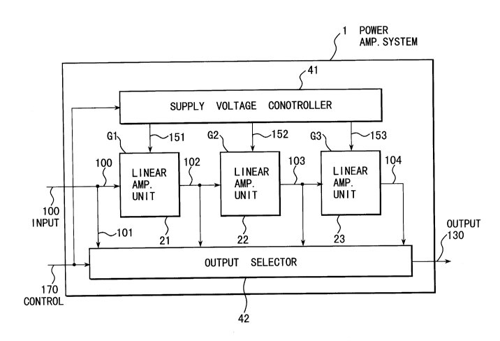
In Fig. 3, apower amplifier system 1 according to a first
embodiment of the invention includes first, second and third
linear (class-A) amplifier units 21, 22 and 23 which are located
a first, second, and third stages, and which are connected in
cascade. The amplifier units 21, 22 and 23 have fixed gains G1,
G2, and G3, respectively, where G1 > 1, G2 > 1, and G3 > 1.
- 2~8;97 18
The power amplifier system 1 further includes a supply
voltagecontroller41forcontrollingthesupplyorstopofapower
supply voltage to the first to third linear amplifier units 21,
22 and 23, and an output selector 42 for selecting a signal to
be outputted. The supply voltage controller 41 and the output
selector 42 are respectively operated in response to a control
signal 170.
An initial input signal 100 to be amplified is inputted
into the power amplifier system 1. The initial input signal 100
is first inputted into the first amplifier unit 21. At the same
time, the initial input signal 100 is inputted into the output
selector 42 as a non-amplified signal 101.
The first amplifier unit 21 amplifies the initial input
signal 100 at the gain G1, outputting a first output signal 102.
The first output signal 102 is then inputted into the second
amplifier unit 22 and the output selector 42. The signal 102 has
a gain of G1 with respect to the initial input signal 100.
The second amplifier unit 22 amplifies the first output
signal 102 at the gain G2, outputting a second output signal 103.
The signal 103 has a total gain of (Gl-G2) with respect to the
initial input signal 100. The second output signal 103 is then
inputted into the third amplifier unit 23 and the output selector
42.
The third amplifier unit 23 amplifies the second output
-18-
2189~18
signal 103 at the gain G3, outputting a third output signal 104.
The signal 104 has a total gain of (Gl-G2-G3) with respect to the
initial input signal 100. The third output signal 104 is then
inputted into the output selector 42.
The output selector 42 has a function of selecting one
of the non-amplified signal 101, and the three amplified signals
102, 103 and 104 and of outputting the selected one as an output
signall30Ofthepoweramplifiersystemlaccordingtothecontrol
signal 170.
The supply voltage controller 41 has a function of
switching the supply and stop of the power supply voltage to the
three amplifier units 21, 22, and 23 according to the control
signal 170.
Next, the operation of the power amplifier system 1
according to the first embodiment is described below.
If the output signal 130 is at an extremely low level,
the control signal 170 sends an order for stopping the supply
voltage to all of the linear amplifier units 21, 22, and 23 to
the supply voltage controller 41. In response to this order, the
supplyvoltagecontroller41stopsthesupplyofthesupplyvoltage
to the amplifier units 21, 22, and 23.
At the same time, the control signal 170 sends an order
for selecting the non-amplified signal 101 to the output selector
42. In response to this order, the output selector 42 selects and
-19-
218971~
outputs the signal 101 as the output signal 130 of the power
amplifier system 1.
In this case, the total gain G of the power amplifier
system 1 is unity, i.e., G = 1.
If the output signal 130 is at a low level, the control
signal 170sends an order forsupplying the supply voltage to only
thefirstlinearamplifierunit21tothesupplyvoltagecontroller
41. In response to this order, the supply voltage controller 41
supplies the supply voltage to the first amplifier unit 21. The
first amplifier unit 21 outputs the first amplified output signal
102.
At the same time, the control signal 170 sends an order
for selecting the amplified output signal 102 to the output
selector 42. In response to this order, the output selector 42
selects and outputs the signal 102 as the output signal 130 of
the system 1.
In this case, the total gain G of the power amplifier
system 1 is G1 greater than unity, i.e., G = G1 > 1.
If the output signal130 is at amiddle level, the control
signal 170 sends an order for supplying the supply voltage to the
first and second linear amplifier units 21 and 22 to the supply
voltage controller 41. In response to this order, the supply
voltage controller 41 supplies the supply voltage to the first
and second amplifier units 21 and 22. The first amplifier unit
-20-
- als9l ~
21 outputs the first amplified output signal 102 and
simultaneously, the second amplifier unit 22 outputs the second
amplified output signal 103.
At the same time, the control signal 170 sends an order
forselectingthesecond amplifiedoutputsignal103 to theoutput
selector 42. In response to this order, the output selector 42
selects and outputs the signal 103 as the output signal 130 of
the system 1.
In this case, the total gain G of the power amplifier
system 1 is (Gl-G2), i.e., G = Gl-G2 > G1.
If the output signal 130 is at a high level, the control
signal 170 sends an order for supplying the supply voltage to all
of the first to third linear amplifier units 21, 22 and 23 to the
supplyvoltagecontroller41.Inresponsetothisorder, thesupply
voltage controller 41 supplies the supply voltage to all of the
first to third amplifier units 21, 22 and 23. The first, second,
and third amplifier units 21 outputs the output signals 102, 103,
and 104, respectively.
At the same time, the control signal 170 sends an order
for selecting the third amplified output signal 104 to the output
selector 42. In response to this order, the output selector 42
selects and outputs the signal 104 as the output signal 130 of
the system 1.
In this case, the total gain G of the power amplifier
( 8
system 1 is (Gl-G2-G3), i.e., G = Gl-G2-G3 > Gl-G2.
With the power amplifier system 1 according to the first
embodiment of Fig. 3, when the required levelof the output signal
130 is extremely low, all of the linear amplifier units 21, 22
and 23 are not supplied with the power supply voltage and they
do not perform their amplification operations. Therefore, the
power consumption is limited to an extremely low level.
Also, ifignoringthesignalattenuationduetothesignal
selection in the output selector 42, the signal-to-noise ratio
(S/N) does not degrade, because the input signal 100 itself is
outputted as the output signal 130 without amplification.
When the required level of the output signal 130 is high,
all of the linear amplifiers 21, 22 and 23 are supplied with the
power supply voltage and they perform their amplification
operations.Thethirdoutputsignal104isselectedtobeoutputted
as the output signal 130 of the power amplifier system 1 by the
output selector 42.
When the required level of the output signal 130 is in
a middle range, only the first linear amplifier unit 21 or the
combination of the first and second linear amplifier units 21 and
22 areselectivelysuppliedwiththepowersupplyvoltage, thereby
performing the amplification operation. The first or second
amplified output signal 102 or 103 is selectively outputted as
the output signal 130 of the system 1 by the output selector 42.
2189718
Since one or two of the linear amplifier units 21, 22 and
23 are selectively supplied with the power supply voltage
accordingtotherequiredleveloftheoutputsignal130, thepower
consumption is limited to a level corresponding to the required
level of the output signal 130.
Further, unlike the conventional amplifier systems of
Figs. 1 and 2, the bias is not changed during operation and
therefore, each of the first to third linear amplifier units 21,
22, and 23 is able to be independently optimized in its bias and
load (or output) impedance. As a result, the input/output
impedance is able to be matched with the output/input impedance
at adjacent stages of each amplifier unit 21, 22, or 23 without
the use of a variable impedance matching unit. This means
that no degradation of the power transmission efficiency takes
~5 place andthat the operation ofthe units 21, 22, and23 is stable.
Additionally, the three amplifier units 21, 22 and 23 are
connected in cascade and the total gain of these units 21, 22,
and 23 is changed by selectively activating the units 21, 22 and
23. Accordingly, the output power of the system 1 can be changed
~0 within a wide range.
Fig. 4 shows anexampleofthe first linearamplifierunit
21. The second and third linear amplifier units 22 and 23 have
the same configuration as that of the first linear amplifier unit
21 and therefore, the description about the second and third
-23-
~ ~ ~q 71g
ampllfier units 22 and 23 is omitted here for the sake of
simplification.
As shown in Fig. 4, the first linear amplifier unit 21
has a linear (class-A) amplifier circuit 21b, an input-impedance
matchingunit 21a, and an output-impedance matching unit 21c. The
amplifier circuit 21b is optimized and fixed in its bias and load
(oroutput) impedancetotherebyrealizeitsmaximumoutputpower.
The input-impedancematchingunit21a servesto matchthe
input impedance of the amplifier clrcuit 21b with the output
impedance of a component or circuit (not shown) at a prior,
adjoining stage to the first linear amplifier unit 21, thereby
avoiding the power loss due to impedance mismatching.
The output-impedance matching unit 21c serves to match
the output impedance of the amplifier circuit 21b with the input
impedance of the second amplifier unit 22 at the next, adjoining
stage of the first linear amplifier unit 21, thereby avoiding the
power loss due to impedance mismatching.
Any other configuration than that shown in Fig. 4 may be
used for the invention.
SECOND EMBODIMENT
Fig. 5 shows a power amplifier system 2 according to a
second embodiment of the invention, which has the same
configuration as that of the first embodiment except for two-
mode linear amplifiers 24, 25, and 26 and an operation-mode
-24-
- '-2 1 ,~ 97 1f8
-
selector 43. Therefore, the description relating to the same
configuration is omitted here by adding the same reference
characters or numerals to the corresponding elements for the sake
of simplification.
S As shown in Fig. 5, the power amplifier system 2 includes
first, second and third linear (class-A) amplifier units 24, 25
and 26 which are located a first, second, and third stages,
respectively. The units 24, 25, and26 are cascade-connected. The
amplifier units 24, 25 and 26 have fixed gains G4, G5, and G6
greater than unity, respectively, i.e., G4 > 1, G5 > 1, and G6
> 1. Each of the amplifier units 24, 25, and 26 has two operation
modesofan amplification mode andapass-throughmode, bothmodes
of which are selectively performed.
The power amplifier system 2 further includes an
operation-mode selector43 forselectingoneofthe amplification
mode and the pass-through mode of the three amplifier units 24,
25, and 26 in response to the control signal 170.
The initial input signal 100 to be amplified is inputted
into the power amplifier system 2. The initial input signal 100
is first inputted into the first amplifier unit 24. Unlike the
first embodiment, the initial input signal 100 is not inputted
into the operation-mode selector 43.
The first amplifier unit 24 amplifies the initial input
signal 100 at the gain G4, outputting a first amplified output
-25-
2~ i4
signal 102a in the amplification mode. The first amplifier unit
24 outputs a first non-amplified output signal 102b without
amplification ofthe initial inputsignal 100 in thepass-through
mode. These two operation modes are alternately performed
according to a control signal 161 sent from the operation-mode
selector 43. The first amplified or non-amplified output signal
102a or 102b is then inputted into the second amplifier unit 25.
None of the output signals 102a and 102b is inputted into the
selector 43.
The second amplifier unit 25 amplifies the first
amplified or non-amplified output signal 102a or 102b at the gain
G5, outputtingasecondamplifiedsignal103aintheamplification
mode and a second non-amplified signal 103b in the pass-through
mode. The second amplified output signal 103a has a total gain
of (G4-G5) or G5 with respect to the initial input signal 100.
The second non-amplified signal 103b has a total gain of G4 or
1 with respect to the initial input signal 100.
The third amplifier unit 26 amplifies the second
amplified or non-amplified output signal 103a or 103b at the gain
G6, outputting a third amplified output signal 104a in the
amplification mode and a third non-amplified output signal 104b
in the pass-through mode. The third amplified output signal 104a
hasatotalgainof(G4-G5-G6), (G4-G6), (G5-G6), orG6withrespect
to the initial input signal 100. The second non-amplified signal
-26-
218971~
103b has a total gain of (G4-G5),G4, G5, or 1 with respect to the
initial input signal 100.
The third amplified or non-amplified output signal 104a
orlO4bisoutputtedastheoutputsignall30Ofthepoweramplifier
system 2.
The operation-mode selector 43 has a function of
selecting one of the amplification mode and thepass-through mode
for each of the first, second, and third amplifier units 24, 25,
and 26 in response to the control signal 170.
Fig. 6shows anexampleofthe first linearamplifierunit
24. The second and third linear amplifier units 25 and 26 have
the same configuration as that of the first linear amplifier unit
24. As shown ln Fig. 6, the linear amplifier unit 24 has a
configuration corresponding to the combination of the linear
amplifier unit 21 as shown in Fig. 4 with two switches 24a and
24b, and a bypassing path 24c.
The switches 24a and 24b are synchronously driven by the
control signal 161 sent from the operation-mode selector 43,
thereby sending the initial input signal 100 to either the linear
amplifier unit 21 or to the bypassing path 24c.
When the amplification mode is selected, the linear
amplifier unit 21 is selected by the switches 24a and 24b. The
initial input signal 100 is inputted into the unit 21 and is
amplified at the gain G4, thereby outputting the first amplified
~i8~1B
-
output signal 102a. On the other hand, when the pass-through mode
is selected, the bypassing path 24c is selected by the switches
24a and 24b. The initial input signal 100 is bypassed through the
unit 21, therebyoutputtingthe firstnon-amplifiedoutputsignal
102b without amplification.
For the second and third linear amplifier units 25 and
26, the same explanation as above is applied.
Next, the operation of the power amplifier system 2
according to the second embodiment is described below.
If the output signal 130 is at an extremely low level,
the control signal 170 sends an order for stopping the supply
voltage to all of the linear amplifier units 24, 25, and 26 to
the supply voltage controller 41. In response to this order, the
supplyvoltagecontroller41stopsthesupplyofthesupplyvoltage
to the amplifier units 24, 25, and 26.
At the same time, the control signal 170 sends an order
for selecting the pass-through mode with respect to all of the
linear amplifiers 24, 25, and 26 to the operation-mode selector
43.Inresponsetothisorder,theoperation-modeselector43sends
the control signals 161, 162, and 163 to the corresponding linear
amplifier units 24, 25, and 26, respectively. As a result, the
initial input signal 100 is outputted as the output signal 130
ofthepoweramplifiersystem2throughthethree linearamplifier
units 24, 25, and-26 without amplification.
-28-
- 2189718
In this case, the total gain G of the power amplifier 2
is unity, i.e., G = 1.
If the output signal 130 is at a low level, the control
signal 170sends anorder for supplying the supply voltage to only
thefirstlinearamplifierunit24tothesupplyvoltagecontroller
41. In response to this order, the supply voltage controller 41
supplies the supply voltage to the first amplifier unit 24.
At the same time, the control signal 170 sends an order
for selecting the amplification mode with respect to the first
amplifier unit 24 and the pass-through mode with respect to the
second and third linear amplifier units 25 and 26 to the
operation-mode selector 43. In response to this order, the
selector 43 sends the control signals 161, 162, and 163 to the
linear amplifier units 24, 25, and 26, respectively.
As a result, the initial input signal 100 is amplified
by the first amplifier unit 24 at the gain G4. The first amplified
output signal 102a, which is outputted from the first amplifier
unit 24, then passes through the second linear amplifier unit 25
without amplification, thereby outputting the second non-
amplified output signal 103b. The second non-amplified output
signal 103b, which is outputted from the second amplifier unit
25, thenpassesthroughthethirdlinearamplifierunit26without
amplification, therebyoutputtingthethirdnon-amplifiedoutput
signal 104b.
-29-
'-- 2189718
In this case, the total gain G of the power amplifier
system 2 is equal to G4, i.e., G = G4.
If the output signal 130 is in a middle range, the control
signal 170 sends an order for supplying the supply voltage to the
first and second linear amplifier units 24 and 25 to the supply
voltage controller 41. In response to this order, the supply
voltage controller 41 supplies the supply voltage to the first
and second amplifier units 24 and 25.
At the same time, the control signal 170 sends an order
for selecting the amplification mode with respect to the first
and second linear amplifier units 24 and 25 and the pass-through
mode with respect to the third linear amplifier unit 26 to the
operation-mode selector 43. In response to this order, the
selector 43 sends the control signals 161, 162, and 163 to the
linear amplifier units 24, 25, and 26, respectively.
As a result, the initial input signal 100 is amplified
bythe first amplifierunit24 atthe gain G4, outputtingthe first
amplified output signal 102a. The first amplified output signal
102a is amplified by the second amplifièr unit 25 at the gain G5,
outputting the second amplified output signal 103a. Then, the
second amplified output signal 103a passes through the third
linear amplifier unit 26 without amplification, thereby
outputting the third non-amplified output signal 104b.
In this case, the total gain G of the power amplifier
-30-
~ lgqll~
system 2 is equal to (G4-G5)., i.e., G G4~5.
If the output signal 130 is in a high level, the control
signal 170 sends an order for supplying the supply voltage to the
first, second and third linear amplifier units 24, 25, and 26 to
the supply voltage controller 41. In response to this order, the
supply voltage controller 41 supplies the supply voltage to the
first, second, and third amplifier units 24, 25, and 26.
At the same time, the control signal 170 sends an order
for selecting the amplification mode with respect to the first,
second, and third linear amplifier units 24, 25, and 26. In
response to this order, the selector 43 sends the control signals
161, 162, and 163 to the linear amplifier units 24, 25, and 26,
respectively.
As a result, the initial input signal 100 is amplified
bythe firstamplifierunit24 at the gain G4, outputtingthe first
amplified output signal 102a. The first amplified output signal
102a is amplified by the second amplifier unit 25 at the gain G5,
outputting the second amplified output signal 103a. The second
amplified output signal 103a is amplified by the third amplifier
unit 26 at the gain G6, thereby outputting the third amplified
output signal 104a.
In this case, the total gain G of the power amplifier
system 2 is equal to (G4-G5-G6)., i.e., G = G4-G5-G6.
-31-
- 2189718
With the power amplifier according to the second
embodiment of Fig. 5, when the required revel of the output signal
130 is extremely low, all of the linear amplifiers 21, 22 and 23
are not supplied with the power supply voltage and they do not
perform their amplification operations. Therefore, the power
consumption is limited to an extremelylow level. This is the same
as that of the first embodiment.
Also, ifignoringthesignalattenuation duetothesignal
selection in the amplifier units 24, 25, and 26, the signal-
to-noise ratio (S/N) does not degrade, because the input signal
lOOitselfisoutputtedwithoutamplificationastheoutputsignal
130 of the system 2. This also is the same as that of the first
embodiment.
When the required level of the output signal 130 is high,
all of the linear amplifiers 24, 25 and 26 are supplied with the
power supply voltage and they perform their amplification-mode
operations. The third amplified output signal 104a is outputted
as the output signal 130 of the power amplifier system 2.
When the required level of the output signal 130 is in
a middle range, only the first linear amplifier unit 21 or the
combination of the first and second linear amplifier units 21 and
22 is/are selectively supplied with the power supply voltage and
it/they perform its/their amplification-mode operation or
operations. The first amplified output signal 102a or the first
-32-
21897~8
amplified output signal 103a is outputted as the output signal
130 of the power amplifier system 2.
Since one or two of the linear amplifier units 24, 25 and
26 are selectively supplied with the power supply voltage
accordingtotherequiredleveloftheoutputsignal130, thepower
consumption is limited to a level corresponding to the required
level of the output signal 130.
Further, each ofthe first to third linear amplifiers 24,
25, and26isindependentlyoptimizedinitsbiasandloadoroutput
impedance and therefore, the input/output impedance is able to
be matched with the output/input impedance at adjacent stages of
each amplifier unit 21, 22, or 23 without the use of a variable
impedance matching unit. This means that no degradation of the
power transmission efficiency takes place and that the operation
of the units 24, 25, and 26 is stable.
Additionally, the three linear amplifier units 24, 25,
and 26 are cascade-connected and the overall gain of these units
24, 25, and 26 is changed by selectively activating the units 24,
25, and 26. Accordingly, the output power of the system 2 can be
changed within a wide range.
THIRD EMBODIMENT
Fig. 7 shows a power amplifier system 3 according to a
third embodiment of the invention, which has a configuration
corresponding to the combination of the power amplifier system
7 l ~
laccordingtothefirstembodimentwitha~afi~bl~e gainamplifier
10 locatedat aprior, adjoining stage to the system 1. Therefore,
thedescriptionrelatingtothepoweramplifiersystemlisomitted
here by adding the same reference characters or numerals to the
corresponding elements for the sake of simplification.
With the power amplifier system 3 according to the third
embodiment, an additional advantage that the level of the output
signal 130 can be changed at narrower intervals is obtained,
because theinputlevelofthesystemlis changedbythe amplifier
10.
If the gains G1, G2, and G3 of the linear amplifier unlts
21, 22, and 23 are designed to be equal to 10 dB, the overall gain
of the system 1 varies in steps for every 10 dB, i.e., G = 0, 10,
20, and 30 dB. If the variable gain Gv of the variable-gain
amplifier 10 is in the range from 0 to 10 dB (or greater), the
overall gain G' of the power amplifier system 3 is expressed as
(Gv + G). This overall gain G' varies in steps for every narrower
value than 10 dB.
FOURTH EMBODIMENT
Fig. 8 shows a power amplifier system 4 according to a
fourth embodiment of the invention, which has a configuration
corresponding the combination of the power amplifier system 2
according to the second embodiment and the variable-gain
amplifier 10 shown in Fig. 7.
-34-
21897 1~
The same additional advantage as that of the third
embodiment can be obtained.
FIFTH EMBODIMENT
Fig. 9 shows a power amplifier system 5 according to a
fifth embodiment of the invention, which corresponds to one
obtainedby replacing the variable-gain amplifier 10 in the third
embodiment of Fig. 7 with a variable attenuator 11.
The variable gain Gv of the variable-gain amplifier 10
of Fig. 7 is replaced with the variable attenuation coefficient
Avofthe attenuator 11. Therefore, the same additional advantage
as that of the third embodiment can be obtained.
Additionally, the variable attenuator 11 may be located
at a subsequent, adjoining stage to the power amplifier system
1.
SIXTH EMBODIMENT
Fig. 10 shows a power amplifier 6 according to a sixth
embodiment of the invention, which corresponds to one obtained
by replacing the variable-gain amplifier 10 in the fourth
embodiment of Fig. 8 with a variable attenuator 11.
The same additional advantage as that of the fourth
embodiment can be obtained.
Thevariableattenuatorllmaybelocatedatasubsequent,
adjoining stage to the power amplifier system 2.
-35-
- 21g971 8
In the above embodiments, the three linear amplifier
units are provided at three stages. However, it is needless to
say that the invention is not limited to this configuration and
the numberofthe linearamplifierunitsmaybe two, four, ormore.
While the preferred forms of the present invention have
been described, it is to be understood that modifications will
be apparent to those skilled in the art without departing from
thespiritoftheinvention.Thescopeoftheinvention,therefore,
is to be determined solely by the following claims.
-36-