Note: Descriptions are shown in the official language in which they were submitted.
2189 ~ 2
RCA 87,553
A METHOD AND APPARATUS FOR GENERATING
VARIABLE RATE SYNCHRONIZATION SIGNALS
The present invention is related to the generation of synchronizing
s signals having different frequencies, a particular example of vvhich
provides different
frame synchronization rates for display of the different modes. of video
signal
conveyed in MPEG compressed form. MPECi herein refers to compression standards
sponsored by the Motion Picture Experts Group of the International
Standardization
Organization or 150.
The invention will be described in the environment of an MPEG video
signal receiver, but should not be considered to be limited to either the use
with video
signals or to MPEG signal processing systems.
The MPEG standards for compressed video signal are extremely
flexible in that video signals having different display modes rrray be
compressed and
is transmitted. For example, source signals of different respective frame
rates may be
compressed and compatible receivers are expected to be capable of reproducing
and
displaying the respective signal at the appropriate frame rate. In particular,
the Grand
Alliance High Definition Television system currently undergoing exarrrination
by the
FCC, accommodates MPEG compressed video signals having frame rates of
2o 29.97002997... Hz or 30.00000(1 Hz. The compressed signal includes a data
field
indicating the frame rate of the received signal, and Grand Alliance compliant
receivers, responsive to this data field are adaptively re configured to
display the
received signal at the indicated L~rame rate.
System level MPECi compressed signal incorporates
2s ;synchronization signals in the form of time stamps. These time stamps are
referenced to a video signal compressor system clock signal of 27 MHz. One
of these time stamps, designated the Presentation Time Stamp or PTS, occurs
un the video level of compressed signal, is synchronized with the occurrence
of
frames of the source signal being compressed, and is determinative of the
RCA 87,553
precise time a decompressed frame is to be displayed by
respective receivers. A second time stamp, designated the System
C'.lock Reference or SCR is incorporated in the system level of the
compressed signal. At the system level, the compressed video
signal is segmented into discreet packets. SCR's arf: included in
ones of these packets, which SCR's are indicative of the precise
time the associated packet is formed/transmitted. The SCR's are
utilized by respective receivers to synchronize a system clock in
the receiver to the system clock in the compression apparatus.
Synchronization of the receiver system clock to the
compression apparatus system clock minimizes the amount of
memory required in respective receivers to rate buffer the
received signal. The receiver system clock is nominally utilized by
the decompression apparatus for decoding the compressed signal.
Since the receiver system clock is synchronous with the
compression apparatus system clock, to which the PTS's are
referenced, the display of the decoded signals may also be timed
via the receiver system clock. However, there are disadvantages
in using a signal clock reference in broadcast signal receivers. For
2 0 example, not infrequently transmitted data may be lost or
corrupted, and error concealment processes must be performed on
the decompressed signal. These processes tend to disrupt the
normal flow of decoded data, and possibly prevent normal display
of frames in accordance with associated PTS's. Also, various
2 5 display features, such as freeze frame, may be implemented,
which disrupt the appropriate association of PTS's with the system
clock.
The present invention includes a programmable
synchronizing system for selectively providing synchronizing
3 0 signals at different rates. In a particular embodiment the
programmable synchronizing system is incorporated. in a video
signal decompression system having a first synchronizing system
for developing a system clock signal and a second synchronizing
system for providing video signal display synchronization signals.
3 5 In a specific embodiment, a synchronizing system for selectably
providing svnchronizin~ signals at different rates, includes an
3 RCA 87,553
oscillator and a programmable counter. The programmable
counter is conditioned to alternately count pulses from the
oscillator by first and second divisors to generate t:he
synchronizing signals. The desired synchronization rate is
effectively the average of the counter output resulting from
counting by the alternate divisors.
Brief Description of the Drawings
Figure 1 is a block diagram of a MPEG compatible
1 0 , video signal receiver, embodying the invention.
Figure 2 is a block diagram of a receiver system clock
generator for the Figure 1 receiver.
Figure 3 is a block diagram of a programmable
generator for providing video signal display synchronizing signals,
embodying the invention. .
Figures 4, 7 and 8 are block diagrams of alternative
programmable sync generators for providing video signal display
synchronizing signals embodying the invention.
Figures 5 and 6 are block diagrams of alternative
2 0 programmable dividers which may be implemented in the
Figure 4 apparatus.
Figure 9 is a flow chart illustrating the programming of
the programmable counter for generating vertical synchronizing
signals in the Figure 8 apparatus.
Referring to Figure 1, transmitted compressed video
signal, e.g. MPEG compatible signal, is detected in an antenna 10
and applied to a tuner-demodulator 11. The tuner-demodulator
11 may include equalization circuitry and an analog-to-digital
3 0 converter. The tuner-demodulator, under control of a system
controller 1 fi, tunes to a desired channel, detects and demodulates
a desired frequency carrier and provides a baseband digital signal
to a forward error correction circuit 12. The circuit 12 may
include Reed-Solomon error correction and trellis decoding
3 5 circuitry for correcting transmission induced errors in the
4 RCA 87,553
received signal. Error corrected signal is applied to an inverse
transport processor 13.
The inverse transport processor, performs a number of
functions including separating desired compressed signal packets
from a time multiplexed packet stream, extracting packet
payloads from selected packets, decrypting encrypted signal
payloads, rate buffering selected signals and generating the
receiver system clock. A detailed description of exemplary
inverse transport processor circuitry may be found in U.S. Patent
No. 5,459,789. Separated compressed audio signal is applied to an
audio signal decompressor 15, separated compressed video signal
is applied to a video decompressor 14, and separated data signal,
such as a program guide, is applied to the system controller 16,
which may include a microprocessor.
The video signal decompressor includes circuitry
which cooperates with decompression memory 17 to decompress
the received video signal. Decompressed video signal is loaded in
a portion of memory 17 where it is available for display at the
appropriate frame rate. In this example the decompressor 14 also
2 0 includes a display clock generator according to the present
invention. The display clock generator provides pixel rate,
horizontal line rate and field/frame rate signals. The pixel rate
signals are used to at least read decompressed signal from the
display memory, and may be used in the decompression process
2 S per se. The line and field/frame rate signals are applied to
deflection circuitry 20 which generates signals for application to
display apparatus (not shown).
Decompressed video signal from the memory 17 is
applied to a signal translator 18 which includes circuitry to
3 0 reformat signal for display. For example the translator may
contain apparatus to convert 4:2:0 format video signal to 4:2:2
format, and to convert non-interlaced signal to interlaced signal
etc.
Translated signalprovided from element18 is in Y,
3 5 R-Y and B-Y format.These signals are applied color matrix
to a 19
which generates digitalR, and B signals and include
G may
RCA 87,553
contrast, brightness and color correction controls. The digital R, G
and B signals are applied to digital-to-analog circuitry 21 which
converts the respective R, G and B signals to analo~; form for
application to display driver circuitry (not shown).
Figure 2 illustrates an exemplary receiver
system clock generator 25. In this embodiment, data from the
forward error correction circuitry 12 is coupled to an inverse
transport processor 32, and a SCR packet detector 31. The inverse
transport processor 32 separates transport packet header data
1 0 from the respective transport packet payloads. Responsive to the
transport header data, the inverse transport processor 32 applies
video signal payloads (designated here as service data 1 ) to, for
example, video decompression apparatus 14, and auxiliary data
(designated as service data 2) to the appropriate auxiliary data
processing elements such as the system controller 16, for example.
SCR's which are typically included in the auxiliary data are routed
to- and stored in a memory element, 34.
The SCR packet detector 31, which may be a matched
filter arranged to recognize appropriate flags in transport packet
2 0 headers, produces a control pulse on the occurrence of transport
packets containing an SCR. The control pulse is applied to a latch
35, which, responsive to the control pulse, stores the count value
currently exhibited by the local counter 36. The local counter 36
is arranged to count pulses provided by e.g., voltage controlled
2 S oscillator 37. The counter 36 is arranged to count modulo the
same number as a counterpart counter in the signal encoder
apparatus (not shown) which produces the SCR contained in the
transport packet.
The voltage controlled oscillator 37 produces the
3 0 receiver system clock signal, which is typically at 2 7 MHz. This
oscillator is controlled by a low pass filtered error signal provided
by a clock controller 39. The error signal may be generated in the
following manner. Designate the SCR arriving at time n as SCRn
and designate the count value concurrently stored in latch 35 as
3 5 L,n. The clock controller reads the successive values of SCR's and
L,'s and forms an error signal E proportional to the differences
2189812
6 RCA 87,553
E ~ ~S CRn - SCR"_ 1 I - ILn - Ln_ 1 I
The error signal E, is utilized to condition the voltage controlled
oscillator 37 to exhibit a frequency which tends to null the error
signal E. The error signal produced by the clock controller 39 may
be in the form of a pulse width modulated signal, and the low pass
filter 38 may be realized in analog components.
In an alternative arrangement, the counter 36 may be
initialized, on start up, to exhibit a count value equal to the first
detected SCR. Thereafter an error signal may be generated
1 0 proportional to the differences (SCRs - L"). However this
arrangement requires a significantly more complicated counter
circuit, as well as routing circuitry to apply the first received SCR
to the counter.
For either arrangement, the free running frequency of
the voltage controlled oscillator must be quite close to the
frequency of the system clock in the encoder/compressor.
In Figure 2, a second clock generator 26. is included.
The clock generator 26 cooperates with a VCXO as chown in the
FIGURE 4 apparatus to generate a pixel display clock. Operation of
2 0 the clock generator 26 is similar to operation of the clock
generator 25, and therefore its operation will not be described in
detail.
Refer to Figure 3 which illustrates a first example of
the display clock generator incorporated in the video
2 5 decompressor 14. Despite the display clock generator being
separate from the system clock, it is advantageous that it be
synchronized to the system clock. This is accomplished in Figure 3
by phase locking the display clock with the 27 MHz receiver
system clock.
3 0 In Figure 3 the different synchronizing (frame) rates
are produced by dividing the system clock which is phase locked
to the display clock generator by different factors. This division is
accomplished by a programmable divider 301, which under
control of the decompressor controller divides the system clock by
3 5 a value N. The value N is selected dependent upon the desired
7 RCA 87,553
frame rate. For example, if the desired display frame rate is
30.000000 Hz, the selected value N is 1000. Alternatively, if the
desired display frame rate is 29.97002997. . . Hz, the selected
value N is 1001.
The divided system clock signal is applied to a first
input terminal of a phase comparator 302 included in a phase
locked loop consisting of a loop filter 303, a voltage controlled
oscillator 304 and a divide by M circuit 305. The phase locked
loop is of conventional design and person's skilled in the art of
signal processing will understand its operation. The output
frequency of the VCO 304 and the value of factor M in the divide
by M circuit 305 will be determined by the desired. pixel clock
frequency. For example, if the pixel clock frequency is chosen at
74.25 MHz, the value M will be 2750.
To generate the appropriate frame synchronizing
signal, the pixel clock frequency is applied to a further divider in
circuit 306. Assuming 2200 pixels per line, the 74.;25 MHz clock is
divided by 2200 to generate a 33.750 KHz line rate signal. Finally
assuming 1125 lines per frame, the line rate signal is applied to a
2 0 second count down circuit, in circuit 306, to divide the line rate
signal by 1125 to generate the frame rate signal.
The Figure 3 circuitry generates acceptable pixel clock
and selectable frame rate signals. However, the phase detector
302-loop filter 303 combination undesirably operates with
2 5 relatively low frequency error signals relative to the pixel clock
frequency. A preferred embodiment, which overcomes this
shortcoming is illustrated in Figure 4.
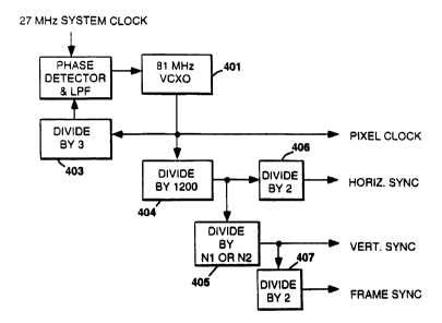
The system of Figure 4 generates a pixel clock signal
which is not subject to significant VCO error signals. In Figure 4,
3 0 the pixel clock is generated by a voltage controlled crystal
oscillator VCXO 401. The output frequency of the VCXO
(illustratively shown as 81 MHz) may be 81 MHz, 74.25 MHz, 27
MHz, etc. and is a system application decision. Because the
oscillator is crystal based, the pixel clock frequency is very stable
3 5 and the frequency deviation is quite small. A system requirement
of a Grand Alliance receiver, for example, is that th.e pixel clock
rx
8 RCA 87,553
frequency vary by no more than 1 part in 1000 regardless of
whether the frame rate is 29.97002997. . . Hz or 30.00 Hz. This
stability is easily satisfied by a VCXO, such as VCXC> 401.
In the Figure 4 arrangement, the display clocks are
indirectly phase locked to the system clock. That is, the output of
the VCXO 401 is phase locked to the encoder or compressor
system clock via SCR's in a manner similar to the :receiver system
clock apparatus for phase locking to the compressor system clock.
This is accomplished in the loop including the divide-by-three
1 0 circuit 403 and the SCR processor 26 (of Figure 2).
The pixel rate clock output by the VCXC) 401 is coupled
to a divide circuit 404. Assuming 1920 active pixels per line or
2400 total pixels per line, the divider 404 is arranged to divide
the pixel rate clock by 1200 to provide a two times line rate
signal. This signal is applied to a divide by two circuit to generate
a horizontal synchronizing signal.
The two times line rate signal is also coupled to a
programmable divider 405. Assuming 1125 lines per frame, the
programmable divider 405 is adjusted to divide the two times line
2 0 rate signal by, for example 1125 to produce a 60 Hz vertical or
field rate signal. The output of divider 405 is coupled to a divide
by two circuit 407 to generate the frame rate synchronizing signal.
It is not possible to divide the two times line rate
signal (or the line rate signal) by a whole number t:o generate a
2 5 frame rate signal of 29.97002997. . . Hz, corresponding to a
59.94005994 Hz vertical signal. In order to generate the
59.94005994 . . . Hz vertical rate signal, the division factor applied
to the programmable divider 405 is periodically changed between
1125 and 1127 lines per frame. If the divisor 112r is
3 0 represented by "0" and the divisor 1127 is represented by " 1 ",
and the divisors applied to the programmable divider 405 occur in
a repeating 16 frame sequence according to the pattern
0000000111111111, the average field rate (vertical rate) will be
exactly 59.95005994 . . . Hz. The repeating 16 frame sequence
3 5 may be rearranged according to the pattern 1010101101010101
i.e.,
RCA 87,553
1010101101010101.1010101101010101.1010101101010101
(where the "." are included only to indicate the demarcation
between sequences) to produce an effective instantaneous
59.94005994 . . . Hz vertical rate. When this alternating divisor
pattern is applied to counter 405, the divide by two circuit 407
provides a 29.97002997 . . . Hz frame rate synchronizing signal.
If interlaced signals are to be produced, vertical or
field rate signals are needed, which signals are generated as
described above. Note, in the above description, the divisors
1 0 applied to the divider 405 are toggled at a frame rate, not the
field rate. The divisors are toggled at the frame rate to insure that
the extra lines which occur in frames produced by division by
1127, are divided between both the odd and even fields.
If the respective decompressor is arranged to output
only non interlaced signal, the divider 404 may be conditioned to
count down by 2400 rather than 1200. In this instance, both
divide by two circuits 406 and 407 are unnecessary. The
programmable divider 405 will directly provide the frame rate
signals.
2 0 Figure 5 illustrates exemplary programmable divider
circuitry which may be toggled between various divisors. A
binary counter 501 is clocked by the two times horizontal rate
signal and reset by the frame rate signal. (For simplicity, it is
assumed that all of the Figure 5 circuits are edge triggered.) The
2 5 parallel output signals provided by the binary counter are applied
to a plurality of decoders 502-504. The respective decoders
provide an output pulse when counter 501 reaches a count value
corresponding to a respective divisor associated with the
respective decoder. For example, decoder 1 may correspond to a
3 0 division by 1125. In this instance, the decoder 1 will output a
pulse on the occasion of the counter 501 outputting a count value
of 1125 indicating the occurance of 1125 pulses of the 2H clock
signal. The outputs of the respective decoders 502-504 are
applied to respective input terminals of a multiplexor 505. The
3 5 output of the multiplexor 505 is the vertical rate signal.
RCA 87,553
The multiplexor 505 is conditioned to couple different
ones of the decoders to its output according to a divisor toggle
pattern. The toggle pattern is selected by the decompressor
controller (or system controller) by controlling a further
5 multiplexor 507.
A plurality of toggle patterns are loaded in a plurality
of shift registers 508-510, each of which contains .an exclusive
pattern. The toggle patterns in the respective shift. registers are a
sequence of control signals for controlling the multiplexer 505.
1 0 These control signals are shifted out of the selected shift register
by the output frame rate signal and applied to respective input
terminals of the multiplexor 507. These patterns are recirculated
in the respective registers via a feedback connection to produce
repetitive toggle patterns. The multiplexor 507 selects one shift
register according to the desired frame rate (toggle pattern). A
toggle pattern may provide a multiplexor 505 control signal to
continuously couple one decoder to its output, or to sequentially
(at the frame rate) couple two or more of the decoder output
connections to the multiplexor 505 output. For the system
2 0 described with respect to Figure 4, the Figure 5 apparatus may
have the plurality of decoders reduced to two, one representing
the divisor 1125 and one representing the divisor :1127. In
addition, only a single toggle pattern register is needed.
Programmable counters of the form illustrated in
2 5 Figure 5 become unwieldy if a large variety of divisors and a large
variety of toggle patterns are desired. Figure 6 illustrates another
form of programmable counter which has greater versatility. In
Figure 6, a programmable down counter 606 is programmed by
values corresponding to respective divisors, via a multiplexor 604.
3 0 T'he multiplexor 604 is toggled at the frame rate by a toggle
pattern loaded in a toggle register 605. The respective
programming values are contained in respective latches 601-603
having respective output connections coupled to the multiplexor
604. The desired programming values and the toggle patterns are
3 5 loaded in the latches 601-603 and the register 605 by either the
system or decompression controller. The decompression
1 1 RCA 87,553
controller, responsive to the compressed video signal, will detect
the frame rate of the current video signal. Responsive to the
detected frame rate, the system will select the appropriate toggle
pattern and divisors stored in system memory (not shown) and
apply them to the appropriate latches 601-603 and the register
605. The register will then be energized to operate the
multiplexer 604 to condition the counter 606 to count in
accordance the desired alternating divisor sequence.
Figure 7 is a programmable synchronizing signal
1 0 generator which is a hybrid of the Figure 3 and Figure 4 circuits.
This circuit includes a VCXO which is synchronized directly to the
2.7 MHz receiver system clock, rather than indirectly as in the
Figure 4 circuit. The operation of the remainder of the Figure 7
embodiment is similar to the operation of elements designated
with like numbers in the Figure 4 circuitry.
The concept of alternating count values or divisors can
be extended to provide other frame rates not producible by whole
number division. However for generating video signal interlaced
frame synchronizing signals, the divisors will preferably be odd
2 0 numbers because of the odd number of lines per interlaced frame.
Instead of toggling between 1125 and 1127, toggling between
divisors 1121 and 1131 may be used. Any frame rate between
30.107 Hz and 29.84 Hz may be supported by appropriate toggling
between divisors.
2 5 Toggling between a larger number of divisors over a
frame sequence will enable generating a larger number of frame
rates. Different sequences of alternative divisors rnay be
employed to produce different frame rates. In addition, a
controller such as a microprocessor may be programmed to
3 0 adaptively apply different divisors not in repeating sequences.
F'or example, consider that it is desired to generate; frame
synchronizing signals which track a non-standard source, which
source provides a frame synchronizing signal. Such a system is
illustrated in Figure 8.
3 5 In Figure 8, a pixel clock is generated by an oscillator
800, which may be a free running crystal oscillator or a controlled
12 RCA 87,553
oscillator in a phase or frequency locked loop as illustrated in the
other embodiments. The pixel clock signal is applied to a first
programmable counter 804. Counter 804, in this instance is
programmable so that a system (such as the Figure 1 system) can
accommodate a variety of pixel per line formats. Counter 804 is
conditioned by the processor 816, which may be a microprocessor
system controller, to divide the pixel clock signal by the
appropriate factor to provide the desired horizontal rate or twice
horizontal rate (2H) signals. That is, on initialization of the system
the processor 816 applies a value corresponding to the divisor to
the latch 802, which value is then loaded into the counter 804
responsive to a jam pulse Jp also provided by the ;processor 816.
C.'ounter 804 provides an output pulse on the occurrence of a
number of pixel clock pulses equal to one half the ;pixel periods of
1 5 a total horizontal line for 2H signal, (or equal to the pixel periods
of a total horizontal line for 1 H signal if so programmed). The
counter 804 is reset by each respective pulse output thereby, and
thus effectively counts modulo W, where W is established by the
value set in the latch 802 .
2 0 The 2H signal is divided down by 2 in divider 806 to
provide the horizontal synchronizing signal. It is also applied as a
clock to a second programmable counter 810. Counter 810 is
conditioned by values set in a latch 808 to divide the 2H signal to
provide a vertical rate signal. The vertical rate signal is divided
2 5 by 2 in circuit 812, to generate a frame synchronizing signal. The
frame synchronizing signal is applied to the input control
terminal Jp of the counter 810 to apply a value corresponding to
the desired divisor to the JAM INPUT port of the counter 810,
each frame period. The value corresponding to the desired
3 0 divisor may be constant or it may be changing.
The frame synchronizing signal is applied to one input
of a comparator 814, shown in this instance as a phase detector. A
reference frame rate signal REF SYNC is applied to a second input
3 5 of the comparator. An output from the comparator is applied to
the processor 816. The processor, responsive to the values
1 3 RCA 87,553
provided by the comparator, generates values corresponding to
the requisite divisor or divisors, and applies same to the latch 808.
Note that new divisors are applied to the counter 810 only after a
full frame count. That is, the counter 810 is not interrupted
during a frame period to update a newly calculated divisor value.
It should be appreciated that since updating the value
corresponding to the divisor during respective frame periods is
not permitted, all but the slowest of processors will have sufficient
time, during respective frame periods, to generate and apply the
necessary sequence of divisor values to the latch 808.
An exemplary algorithm for generating a sequence of
divisor values (or values corresponding to divisor values) is
illustrated by the flow chart of Figure 9. This algorithm applies
one of six different values N1 -N6, corresponding to six different
divisors, to the latch 808 each frame period. The greater/lesser
the frame rate is from the desired frame rate, the. greater/lesser
the applied value, so as to effect faster attack times. Assuming a
pixel clock of 81 MHz and approximately 1125 lines per frame, the
exemplary values Nl - N6 may be N1=1121; N2=1:123; N3=1125;
2 0 N4=1127; NS=1129; N6=1131. This algorithm assumes a system
similar to Figure 8 in which phase difference values ~ are applied
from a phase detector 814 to the controller 816. In the process,
the current phase difference value, ~, is sampled { 900 } and tested
{901 }. If ~ is less than a first threshold value TH1 (indicating
2 5 slight deviation from REF SYNC), it is tested { 902 } for polarity. If
the polarity is positive a value corresponding to divisor N3 is
accessed { 904 } from processor memory and applied to the latch
808, else a value corresponding to divisor N4 is applied { 903 } to
the latch 808. Then the system returns to step { 9017 } to wait for
3 0 the next phase difference signal.
If at step {901 } ~ is greater than the first threshold
value, it is further tested { 905 } against a second larger threshold
value TH2. If ~ is less than the second threshold value TH2
(indicating slightly greater deviation from REF SYNC), it is tested
3 5 { 906 } for polarity. If the polarity is positive a value
corresponding to divisor N2 is accessed { 908 } from. processor
14 RCA 87,553
memory and applied to the latch 808, else a value corresponding
to divisor NS is applied { 907 } to the latch 808. Then the system
returns to step { 900 } to wait for the next phase difference signal.
If at step { 905 } ~ is greater than the second threshold
value TH2 (indicating even greater deviation from R1JF SYNC), it is
tested { 909 } for polarity. If the polarity is positive a value
corresponding to divisor N 1 is accessed { 911 } from processor
memory and applied to the latch 808, else a value corresponding
to divisor N6 is applied { 910 } to the latch 808. Then the system
1 0 returns to step { 900 } to wait for the next phase difference signal.
Variations on this algorithm may easily be derived.
F'or example the phase difference signal may be filtered or
integrated before testing against the various threshold values. In
addition constraints may be placed on the sequence; of values
1 5 applied to the latch. For example, application of t:he larger values
N 1 (N6) may be constrained not to occur twice in successive
frames. As another alternative, once the system ins substantially
synchronized, ones of the values N1-N3 may be forced to alternate
with ones of values N4-NS etc. Another variation may include the
2 0 use to even and odd divisors.
The embodiment of Figure 8 was described in the
environment of a video signal processing system, however, it will
be appreciated by those skilled in circuit arts, that it may be
implemented in a wide variety of systems requiring generation of
2 5 phase or frequency tracking synchronizing signals.