Note: Descriptions are shown in the official language in which they were submitted.
21 8 98 5 1
1
VOLTAGE REGULATOR
BACKGROUND
The present invention concerns voltage regulators, and
more particularly, a voltage regulator wherein the efficiency of
the regulator is improved.
The present voltage regulator is useful in a direct
broadcast satellite receiver system which includes an outdoor
microwave antenna which can be aimed at a satellite to receive a
signal from the satellite. The signal received from the satellite is
amplified by a "low noise block converter" (LNB) mounted in very
close proximity to or on the antenna.
The output signal from the LNB is carried to an indoor
receiver by a coaxial cable. In order to supply power from the
indoor receiver to the LNB, as well as to control the polarization
of the LNB, a DC voltage is multiplexed onto the center conductor
of the coaxial cable. The circuits in the LNB are designed so that
they will function with either a lower power supply voltage or a
higher power supply voltage, with the dual supply voltages being
used to control polarization settings of the LNB, e.g., the lower
voltage selecting right hand circular polarization (RHCP) and the
higher voltage selecting left hand circular polarization (LHCP).
The current drain of the LNB is fairly constant with either of the
regulated power supply voltages.
Voltage regulators, which use a controllable series
impedance device for maintaining a regulated output voltage
coupled to a load, are susceptible to damage if a short circuit or
other fault is applied to the output terminals of the regulator.
Such damage often is caused by excessive thermal dissipation of
the series impedance device or by exceeding the current rating of
WO 95/31762 PCT/US94/10298
2189851
2
the series device. For this reason, it is common to provide
overload protection to prevent such damage to the regulator.
One type of overload protection is current limiting in
what is known as a "foldback" voltage regulator, such as is
disclosed in U.S. Patent No. 3,445,751 of Easter. Such a regulator
provides output voltage regulation for a changing load until an
overload current threshold is reached. For load currents above
this threshold, the available output current decreases as the load
increases, with a corresponding decrease in the output voltage.
1 0 The short-circuit current can be adjusted to be but a small
fraction of the full load current, thus minimizing the dissipation in
the series pass transistor. The voltage regulator of the present
invention is such a "foldback" voltage regulator.
Supply current flows from the DC supply source
1 S through the emitter-collector path of the series pass transistor to
the load. The amount of this current is controlled by a control
signal coupled from the output voltage to the base electrode of
series pass transistor via an amplification transistor and other
circuitry arranged in a negative feedback circuit configuration. In
2 0 this way, with the voltage drop across the emitter-collector path
of the series pass transistor is adjusted to maintain a regulated
output voltage.
The series pass transistor incurs a voltage drop under
full load, and accordingly dissipates power as part of its regulating
2 5 function. It is desirable to minimize this power dissipation in the
series pass transistor to improve reliability of the series pass
transistor, to reduce the cost of the series pass transistor along
with associated heat sinks, and to improve the efficiency of the
regulation at maximum output voltage by minimizing the voltage
3 0 difference between the unregulated input voltage and the
regulated output voltage. .
SUMMARY OF THE INVENTION
Briefly, the present invention concerns a voltage
3 5 regulator wherein the series pass transistor and an amplification
transistor are of complementary types. Supply current flows from
WO 95/31762 PCTIUS94/10298
3
the DC supply source through the emitter-collector path of the
series pass transistor to the load. The amount of this current is
" controlled by a negative feedback control signal coupled from the
regulated output voltage to the base electrode of the amplification
' 5 transistor, which in turn drives the base of the series pass
transistor. The emitter electrode of the amplification transistor is
coupled to a voltage which is less than the regulated DC output
voltage so that drive requirements for the pair of transistors is
reduced.
BRIEF DESCRIPTION OF THE DRAWING
Reference can be had to the drawings wherein:
Figure 1 shows a schematic of a regulator according to
aspects of the present invention.
Figure 2 shows an illustrative modification of a portion
of the regulator of Figure 1.
DETAILED DESCRIPTION OF THE PREFERRED EMBODIMENT
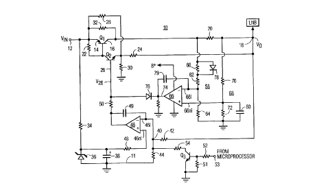
Referring now to Figure 1, there is shown a voltage
2 0 regulator 10 according to aspects of the present invention.
Voltage regulator 10 can be switchable between a higher
regulated DC output voltage mode and a lower regulated DC output
voltage mode.
An unregulated direct current power supply source
2 5 (not shown) is connected between terminal 12 and a reference
potential point 11 (e.g., ground). The emitter electrode 14 of
series pass PNP transistor Q1 is coupled to terminal 12. The
collector electrode 16 of transistor Q 1 is coupled to an output
terminal 18 through resistor 20. A load (LNB) is coupled between
3 0 output terminal 18 and reference point 11 (not shown). The base
electrode of transistor Q 1 is coupled to a collector electrode of NPN
amplification transistor Q2 and to input terminal 12 through a
resistor 22. The emitter electrode of transistor Q2 is coupled to
output terminal 18 through a resistor 24 and to reference point
3 5 11 by resistor 30. The base electrode of transistor Q2 is coupled
it i
WO 95131762 PCT/US94110298
~1898~1
4
to receive a control signal, which will be discussed more fully
below.
Supply current flows from the DC supply source
coupled to terminal 12 through the emitter-collector path of
transistor Q1 and resistor 20 to output terminal 18 and the load.
The amount of this current is controlled by the control signal
coupled to the base electrode of transistor Q2 via line 26, with the
voltage drop across transistor Q 1 being adjusted to maintain a
regulated output voltage at terminal 18. A resistor 32, coupled
1 0 between the emitter and collector electrodes of Q 1, continues to
provide some current to the load even if transistor Q1 is
completely cut-off. Resistor 22, coupled between the emitter
electrode and the base electrode of transistor Q1, reduces the
effects of collector to base leakage currents in transistor Q 1.
1 5 The complementary arrangement of transistors Q 1, Q2
provides both voltage and current gain since the collector
electrode of transistor Q2 is coupled to the base electrode of
transistor Q 1 and the output of the series pass arrangement is
taken from the collector electrode 16 of transistor Q 1. Thus,
2 0 transistors Ql, Q2 are arranged as amplifiers within a feedback
loop with the loop gain determined by a feedback network
comprised of resistor 24 coupled from output terminal 18 to the
emitter electrode of transistor Q2, and resistor 30 coupled to
ground.
2 5 Additionally, the arrangement of transistors Q1, Q2
and resistors 24, 30 has a further advantage of improving the
efficiency of by regulator 10, by reducing power dissipation losses
in Q1 under heavy load conditions, and reducing the drive
requirements for transistors Q1, Q2. Figure 2 shows a portion of
3 0 the series pass arrangement without the resistor divider made up
of resistors 24, 30 (resistor 24 is replaced by a short circuit and
resistor 30 is replaced by an open circuit). In this arrangement,
the voltage at the base of transistor Q2 (line 26), would be 0.7
volts above the voltage Vo at output terminal 18, and due to the
3 5 base-emitter voltage drops in transistors Q1 and Q2, Vo would be
at least 1.4 volts below the input voltage Vin at terminal 12. This
'"" WO 95/31762 I pCT/US94/10298
provides an upper limit to the maximum regulated output voltage
with respect to the unregulated input voltage. Further, the 1.4
volt voltage drop across transistor Q 1 dissipates power in
transistor Q 1.
To have the regulator operate with a lower difference
voltage between the input voltage Vin and the output voltage Vo,
and reduce power dissipation in transistor Q1, it is desirable that
transistor Q1 be driven into saturation at the highest output
voltages in the high voltage mode. Voltage divider resistors 24,
1 0 30 improve the efficiency of the series pass circuit to achieve
these attributes.
Referring back to Figure l, voltage V26, at line 26, is
mathematically expressed as follows:
1 S V26=Vbe of Q2+Vo(resistor 30/(resistor 30+resistor 24)).
If the Vbe of Q2 is 0.7 volts and the value of resistor 24 equals
the value of resistor 30, then:
2 0 V26 = 0.7 volts + Vo/2.
Since this arrangement lowers the voltage at the emitter of
transistor Q2 to substantially below the voltage Vo, it makes it
easier to drive Q2 harder since the voltage V26 can be a lower
2 5 voltage, thus allowing transistor Q1 to be more easily driven into
saturation while still maintaining transistor Q2 in an active non-
saturating state. Thus, with divider resistors 24, 30, the series
pass transistor Q1 can be driven so that Vo = Vin - 0.2 volts (the
typical saturation voltage for transistor Q 1 ) instead of at least 1.4
3 0 voltage, as discussed above. Thus, the regulator can operate with
a lower difference between the input voltage Vin and the output
voltage Vo, and with a resulting reduction in the power
dissipation in transistor Q1 when it is fully driven.
The lower difference between input and output
3 5 voltages is of particular importance in the higher output voltage
mode because the maximum value of voltage Vin is limited.
in r
WO 95/31762 PCTIUS94/10298
6
Additionally, since the control voltage applied to lead 26 is now
considerably lower than B+, operational amplifier 46, which
provides control signal V26, as will be discussed more fully below,
is not required to operate at output voltages near the value of B+
in order to drive transistor Q2 to saturate transistor Q1.
A resistor 28 is coupled between the emitter electrode
14 of transistor Q1 and the emitter electrode of transistor Q2, to
prevent the emitter electrode of Q2 from falling so low when the
output is short circuited, that operational amplifier 46 cannot
1 0 reverse bias the base-emitter junction of transistor Q2 to cut-off
transistor Q1. The ability to cause transistor Q1 to be cut-off is
important for current limiting, which will be discussed more fully
below.
A reference voltage is provided by resistor 34 and
1 5 zener diode 36 connected in series between input terminal 12 and
ground, and the reference voltage is filtered by a capacitor 38.
The reference voltage is coupled to a non-inverting (ni) input
terminal 46ni of an operational amplifier 46 where it is compared
to a divided down version of Vo, which is coupled to an inverting
2 0 (i) input terminal 46i. The divided down version of Vo is derived
from a tap at the junction of series voltage divider resistors 42
and 44 coupled between output terminal 18 and ground 11. The
output signal of amplifier 46 provides the control signal V26 at
line 26 through isolation resistor 50. This arrangement provides
2 5 negative feedback which reduces or increases the drive to
transistor Q1 if there is a respective increase or decrease in the
regulated output voltage Vo. Capacitor 49, coupled between the
output of amplifier 46 and terminal 46i, suppresses oscillation.
Switching between lower and higher output voltage
3 0 modes is made possible by transistor Q3, which can be driven into
saturation by a control signal coupled to its base electrode from a
control unit, (not shown), such as a microprocessor, through
resistor divider 51, 52. The collector electrode of transistor Q3 is
coupled to terminal 46i by resistor 54, and when transistor Q3 is
3 5 driven into saturation, resistor 54 is coupled in parallel with
divider resistor 44, thus modifying the voltage divider ratio of
WO 95/31762 PCT/US94/10298
7
resistors 42, 44. The resulting change in V26, provided by
comparator amplifier 46, causes the output voltage at terminal 18
to be switched to the higher voltage required for LHCP by the
LNB.
Turning now to the foldback current limiting aspect of
the present regulator, a voltage divider 58, comprising series
resistors 60, 62 and 64, is coupled between collector 16 of
transistor Ql and ground, with a tap at the junction of resistors 62
and 64 being coupled to an inverting input terminal 66i of
1 0 operational amplifier 66. A voltage divider 68, comprising series
resistors 70 and 72, is coupled between output terminal 18 and
ground, with a tap at the junction of the resistors 70, 72 being
coupled to a non-inverting (ni) input terminal 66ni of amplifier
66. Output terminal 74 of amplifier 66 is coupled to the cathode
1 5 of a diode 76, with the anode of diode 76 being coupled to control
lead 26. Diode 76 prevents operational amplifier 66 from
effecting V26 during normal operation, as will be discussed more
fully below. Capacitor 79, coupled between output terminal 74
and terminal 66i, suppresses oscillation. Capacitor 80, coupled
2 0 across resistor 72, prevents any AC signal received from the LNB
load from effecting amplifier 66. The component values of the
resistors in dividers 58, 68, are as follows:
resistor 60 = 1K ohms resistor 62 = -3K ohms
resistor 64 = 12K ohms resistor 70 = 2.8K ohms
2 S resistor 72 = 12K ohms
Resistor 20, (3.3 ohms), develops a voltage thereacross
proportional to the output current. Thus, the voltages across
dividers 58 and 68 are slightly different, and the voltages at the
taps of the two dividers are arranged to be slightly different.
3 0 When current drawn through resistor 20 is less than the threshold
foldback current, the action of voltage dividers 58 and 68 is such
that the voltage at terminal 66ni is more positive than the voltage
at terminal 66i, and the output voltage at terminal 74 is at or near
the B+ voltage. This back biases diode 76 and prevents .the output
3 5 of amplifier 66 from interfering with the drive at line 26 under
normal operation. Thus, unless the circuit is in the current
ii
WO 95/31762 ~ PCT/US94/10298
8
limiting mode, normal control of dine 26 is provided by amplifier
46. However, if the current drawn through resistor 20 exceeds
the foldback threshold current, the voltage drop across resistor 20
causes the voltage at the terminal 66ni to be slightly lower than
the voltage at terminal 66i. This forces the output voltage at
terminal 74 to go low due to the large gain of operational
amplifier 66. This causes diode 76 to be forward biased and
cause the operation of amplifier 46 to be overriden so that the
control voltage on line 26 is reduced to nearly zero volts. As a
1 0 result, the output current at terminal 18 is reduced to nearly zero
and output voltage Vo is reduced to nearly zero volts. In this
manner, when the output is short circuited or a fault occurs in the
load, the output current is "folded back" from the nominal output
current which is provided to the load during normal operation.
1 5 For example, the output current may be folded back from a
normal value of 350 milliamperes to about 10 milliamperes.
Thus, transistor Q1 is protected from being subjected to excessive
thermal dissipation or overcurrent condition due to a load fault.
When the load fault is removed, voltage regulator 10 recovers and
2 0 returns to normal operation.
Voltage regulator 10 is a dual voltage voltage
regulator. When the output voltage Vo is changed to the higher
voltage, the foldback threshold current at which current limiting
is initiated, would also be changed. The change in the foldback
2 5 threshold current occurs because the voltage drop across the
current sensing resistor 20 would remain the same for any
particular current, but the differential voltage coupled to input
terminals 66ni and 66i due to the increase in voltage across
voltage dividers 58, 68. This is not desirable since the protection
3 0 afforded transistor Q1 and the load would be reduced.
In the present embodiment, to maintain the same
current limiting threshold in the higher voltage mode, the voltage
division of divider 58 is altered by diode 78 coupled across
resistor 60. The voltage drop across resistor 60 is chosen to be
3 5 less than the threshold of forward conduction of diode 78 in the
lower output voltage mode. However, when regulator 10 is
W O 95131762 i
PCTIUS94/10298
9
switched into the higher voltage mode, the higher voltage drop
across resistor 60 is sufficient to cause diode 78 to conduct in its
forward direction, thus changing the voltage division of divider 58
and the relationship of the difference voltage applied to terminals
' S 66i and 66ni. This change of voltage divider 58 maintains
substantially the same foldback threshold current in the higher
voltage output mode as in the lower voltage output mode. For
example, without the change in voltage divider 58, the current
limiting threshold at the lower regulated output voltage, in the
1 0 exemplary embodiment, would be about 350 ma, and the current
limiting threshold at the higher regulated output voltage would be
about 600 ma. With the change in voltage divider 58, the current
limiting threshold is about 350 ma for each of the dual output
voltages.
15 In the present embodiment, diode 78 is a 1N914 diode
having a reasonably sharp "knee". If it is desired to reduce the
sharpness of the conduction knee, a resistor (not shown) can be
connected immediately in series with diode 78. Alternately, diode
78 can be replaced by a plurality of series connected diodes.
2 0 Other voltage sensitive devices can also be used, such as
germanium diodes, LED's, voltage dependent resistors, or zener
diodes. In the case of an LED, the diode itself may be a visual
indicator as to the operating mode of the regulator. ~ Additionally,
a relay or a switching transistor can be used in place of diode 78.
2 5 In such a case, the presence or absence of a microprocessor signal,
such as available at terminal 53, can be used to initiate the
switching of the divider resistors when that same microprocessor
signal initiates the change in output voltage. Still further, the
voltage sensitive device can be connected elsewhere in one of the
3 0 voltage dividers.
It should be noted that in the exemplary embodiment,
operational amplifiers 46 and 66 are LM348 operational
amplifiers made by National Semiconductor of USA. These
operational amplifiers have PNP input circuits which permit the
3 5 amplifiers to still be operational when the voltages at the input
terminals are very low. However, it has been found that
i,
WO 95131762 PCTIUS94/10298
~~.~r'~8~1
to
operational amplifiers having NPN input circuits, typically are not
operational when the voltages at the input terminals are lower
than about one volt. It has been found that if such NPN input
circuit operational amplifiers are used, the amplifier 66 may latch
in the foldback current limiting mode, i.e., output terminal 74 is
latched to zero output volts, and will not recover to a normal
operating mode when the fault is removed from output terminal
18. However, there may be situations where this latching in a
"fail-safe" mode may be desirable.