Note: Descriptions are shown in the official language in which they were submitted.
CA 02190122 2004-08-20
WO 95131672 PCT/US95/04285
- 1 -
ILLUMINATION SYSTEM EMPLOYING
AN ARRAY OF MICROPRISMS
15
Baclc~ound of the Invention
This invention relates generally to an optical illumination system for
collimating light that provides for relatively high light transmission. More
particularly, the invention is directed to an illumination system having a
plurality of
2 0 optical microprisms and microlenses for redirecting light removed from a
non-
collimated light source and providing either separately or in combination a
non
diffuse or a substantially collimated light source output.
A number of optical and illumination applications require the production of
either a non diffuse or a collimated light source which provides an efficient
output
2 5 of light. Typical problems encountered with collimated light sources
include: 1 ) a
non-uniform tight distribution; 2) a lack of a controlled directional output
of light;
3) inefficiencies with regard to the amount of the collimated light output
versus the
amount of the non-collimated light input; and 4) the lack of an effident
collimated
light source in a compact design or narrow profile.
3 0 Accordingly, there exists a need in the optical and illumination arts to
provide an illumination assembly that provides an energy e»cient light source
while
maintaining a narrow profile.
Summary,of the Invention
3 5 The present invention is directed to an optical illumination system which
provides either separately or in combination a non diffuse or a substantially
W095/3r672 219 ~ ~ ~ ~ PCT~S95104285
- 2 -
collimated light source that is energy efficient (hereinafter referred to as a
spatially
directed tight source). Additionally, this invention is directed to any
lighting
application that requires a low profile spatially directed light source.
The optical illumination system comprises a diffuse input light source in
5, close proximity to a light transmitting means, a reflecting means for
removing and
redirecting the light from the light transmitting means where the reflecting
means
are operatively disposed adjoining said fight transmitting means. The
reflecting
means comprises an array of trticroprisms, or in combination an array of
microprisms in optical cooperation with an array of microlenses whereby the
microprisms are operatively disposed between the light transmitting means and
the
microlenses. The reflecting means of the present invention provide an energy
efficient distribution of spatially directed light that is provided in a low
profile
assembly.
In one preferred embodiment, a single input light source is positioned
IS adjacent to a light accepting surfitce of the light transmitting means. The
light
transmitting means may be any structure that transmits light via reflection,
such as a
light pipe, light wedge, waveguide or any other structure known to those
skilled in
the art. Preferably the tight transmitting means comprises a waveguide that
accepts
the light generated by the input light source and transports the light via
total internal
reflection (T>It). Attached on one face of the waveguide is an array of
microprisms.
The microprisms comprise a light input surface in contact with the waveguide
and a
light output surface distal to and parallel with the light input surface. The
microprisms fluffier comprise four sidewalls. The four sidewalls are angled in
such
a way that light traveling through the waveguide is captured and redirected by
the
microprisms, reflects through the microprisms via TIR and emerges from the
microprisms as a spatially directed fight source. A spatially directed light
source is
meant to include a substantially collimated fight source in a direction
substantially
perpendicular to the to the light output surface or a tight source directed at
an angle
with respect to the normal of the light output surface.
3 0 In an alternate embodiment, an array of ttticrolenses is operatively
disposed
adjacent to the light output surface of the tnicroprisms. The four sidewalls
of each
microprism are angled in such a way that fight from the single light source
traveling
through the waveguide is captured by the microprisms, reflects through the
microprisms via TIR and emerges from the microprisms as a spatially directed
light
WO 95131672 ~ a j 2 ~ PCT/US95104285
- 3 -
source. The microlenses are formed with the proper curvature and positioned so
that the light emanating from each microprism is directed to a corresponding
microlens. The light transmits through the microlenses and emerges as a
substantially collimated light source.
5. In another preferred embodiment two input light sources are positioned
adjacent to oppositely disposed fight accepting surfaces of the light
transmitting
means. The light transmitting means comprises a waveguide that accepts the
light
generated by both input fight sources and transports the light via TIR.
Attached on
one face of the waveguide is an array of microprisms. The microprisms comprise
a
light input surface in contact with the waveguide and a light output surface
distal to
and parallel with the light input surface. The microprisms further comprise
four
tilted sidewalls that are angled in such a way that light traveling in the
waveguide
from both input light sources is captured and redirected by the microprisms,
reflects
through the microprisms via TIR and emerges from the microprisms as a
spatially
directed light source.
In still another alternate embodiment, an array of microlenses is operatively
disposed adjacent to the light output surface of the microprisms. The four
sidewalls
of each microprism are angled in such a way that fight from both light sources
traveling through the waveguide is captured by the microprisms, reflects
through
the microprisms via T1R and emerges from the microprisms as a spatially
directed
light source. The microlenses are formed with the proper curvature and
positioned
so that the light emanating from each microprism is directed to a
corresponding
microlens or a plurality of microlenses. The tight transmits through the
ttticrolenses
and emerges as a substantially collimated light source.
There are many illumination applications that can take advantage of such an
illumination system employing such an arrangement of microprisms and
microlenses. Such applications exist in the automotive industry, the aerospace
industry and the commercial and residential markets. Some automotive
applications, by way of example only and are not intended to limit the
possible
3 0 applications include: low profile car headlights and taillights; low
profile interior car
lights such as reading lights and map lights; light sources for dashboard
displays;
backlights for flat panel navigation displays, flat panel auto TV screens and
flat
panel electronic instrument displays; traffic lights; and backlights for road
signs.
Illustrative examples in the aerospace industry include backlights for flat
panel
WO 95131672 ~ ~ ~ ~ ' PGTlUS95/04285
- 4 -
cockpit displays and flat panel TV screens in the passenger section of the
aircraft;
law profile reading lights and aircraft landing lights; and runway landing
lights.
Residential and commercial applications include low profile interior and
exterior
spotlights and room lighting with a low degree of collimation; backlights for
flat
panel TV screens, LCD displays, such as computers, game displays, appliance
displays, machine displays and picture phones.
Additional objects, advantages and novel features of the invention will be set
forth in part in the description which follows, and in part will become
apparent to
those skilled in the art upon examination of the following or may be learned
by
practice of the invention. The objects and advantages of the invention may be
realized and attained by means of the instrumentalities and combinations
particularly
pointed out in the appended claims.
The above and other objects and advantages of this invention will be
apparent on consideration of the following detailed description, taken in
conjunction
with the accompanying drawings, in which like reference characters refer to
like
parts throughout, and in which:
FIGURE I is an elevation view of one embodiment of the present invention
2 0 in conjunction with a single input fight source;
FIGURE lA is an exploded view of the embodiment of Fig. I;
FIGURE IB is an alternate view of the embodiment of Fig. 1;
FIGURE 2 is an elevation view of the embodiment of Fig. I including an
array ofmicrolenses;
2 5 FIGURE 2A is an alternate view of the embodiment of Fig. 2;
corresponding microlens;
FIGURE 3 is a sectional view of a single microlens;
FIGURE 3A is a plan view of one embodiment of a single microlens;
FIGURE 4 is an elevation view of an alternate embodiment of the present
3 0 invention in conjunction with two input light sources;
FIGURE 4A is an exploded view of the embodiment of Fig. 4;
FIGURE 5 is an elevation view of the embodiment of Fig. 4 including an
array of microlenses;
FIGURE 6 is a exploded view of the embodiment of Fig. 5; and
WO 95/31672 ~ 19 fl ~ 2 2 PCT~S95104285
- 5 -
FIGURE 7 is an alternate view of the embodiment in Fig. 5.
Detailed Description of the Preferred Embod'me~r~
The preferred embodiments of the present invention will be better
5, understood by those skilled in the art by reference to the above figures.
The
preferred embodiments of this invention illustrated in the figures are not
intended to
be exhaustive or to limit the invention to the precise form disclosed. They
are
chosen to describe or to best explain the principles of the invention and its
applicable and practical use to thereby enable others skilled in the art to
best utilize
the invention.
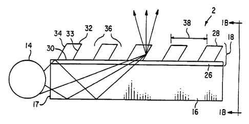
One preferred embodiment of the present invention is shown in Figs. I, LA
and 1B. An illumination system, represented by the number 2, comprises a light
generating means 14, a waveguide 16 having a light accepting surface 17 and a
transparent reflecting means 18 in contact with waveguide 16. Illustrative of
useful
15, light generating means 14 are lasers, fluorescent tubes, light emitting
diodes,
incandescent lights, sunlight and the like. The waveguide 16 is made from any
transparent material such as glass or polymer. In Fig. l, light generating
means l4
is in close proximity to waveguide 16, and reflecting means 18 is in contact
with
wave guide I6.
The reflecting means 18 comprises an optional adhesion promoting layer 26
and an array of microptisms 28. Light reflects through waveguide 16 via TIR
and
enters each microprism 28 by way of light input surface 30, reflects off
sidewalls 33,
35 and 37 and exits the microprism 28 through the light output surface 32 as a
spatially directed light source.
Waveguide 16 is transparent to light within the wavelength range from
about 400 to about 700 nm.. The index of refraction of the waveguide I6 may
range from about 1.40 to about 1.65. The most preferred index of refraction is
from about 1.45 to about 1.60. The waveguide 16 may be made from any
transparent solid material. Preferred materials include transparent polymers,
glass
3 0 and fused silica. Desired characteristics of these materials include
mechanical and
optical stability at typical operation temperatures of the device. Most
preferred
materials are glass, acrylic, polycarbonate and polyester.
Miaoprisms 28 can be constructed from any transparent solid material.
Preferred materials have an index of refraction equal to or greater than
waveguide
W0 95131672 PCT/fJS95104285
2190122
- 6 -
16. Preferred materials have a refractive index between about 1.40 and about
1.65
and include polymethylmethacrylate, polycarbonate, polyester, poly(4-methyl
pentene), polystryrene and polymers formed by photopolymerization of acrylate
monomers. More preferred materials have an index of refraction between abut
1.45
, and about 1.60 and may include polymers formed by photopolymerization of
acrylate monomer mixtures composed of urethane acrylates and methacrylates,
ester
acrylates and methacrylates, epoxy acrylates and methacrylates, (poly)
ethylene
glycol acrylates and methacrylates and vinyl containing organic monomers.
Useful
monomers include methyl methacrylate, n-butyl acrylate, 2-ethylhexyl acrylate,
isodecyl acrylate, 2-hydroxyethyl acrylate, 2-hydroxypropyl acrylate,
cyclohexyl
acrylate, 1,4-butanediol diacrylate, ethoxylated bisphenol A diacrylate,
neopentylglycol diacrylate, diethyleneglycol diacrylate, diethylene glycol
dimethacrylate, 1,6-hexanediol diacrylate, trimethylolpropane triacrylate,
pentaerythritol triacrylate and pentaerythritol tetra-acrylate. Especially
useful are
mixtures wherein at least one monomer is a multifunctional monomer such as
diacrylate or triacrylate, as these will produce a network of crosslinks
within the
reacted photopolymer. The most preferred materials for microprisms 28 formed
by
photolithography are crosslinked polymers formed by photopolymerizing mixtures
of ethoxyiated bisphenol A diacrylate and trimethytolpropane triacrylate. The
index
of refraction of the most preferred materials ranges from about 1.53 to about
1.56.
Other materials that can be used in alternate methods of manufacture, such as
injection molding, include polycarbonate, acrylic and poly(4-methyl pentene).
Microprisms 28 are separated by interstitial regions 36. The index of
refraction of interstitial regions 36 must be less than the index of
refraction of the
microprism 28. Preferred materials for interstitial regions include air, with
an index
of refraction of 1.00 and fluoropolymer materials with an index of refraction
ranging from about 1.16 to about 1.40. The most preferred material is air.
The optional adhesion promoting layer 26 is an organic material that is light
transmissive and that causes the microprisms 28, especially microprisms formed
3 0 from polymers, as for example photocrosslinked acrylate monomer materials,
to
adhere strongly to the waveguide 16. Such materials are well known to those
skilled in the art. The thickness of adhesion promoting Payer 26 is not
critical and
can vary widely. In the preferred embodiment of the invention, adhesion layer
26 is
less than about 30 micrometers thick.
WO 95/31672 219 ~ 12 2 PCT~S95/04285
_ 7 _
The microprisms may be arranged in any pattern on waveguide 16, such as
in a square, rectangular or hexagonal pattern. The microprisms have a repeat
distance 38 (Fig. I) in the direction perpendicular to light accepting surface
17 and
repeat distance 40 (Fig. LB) in the direction parallel to light accepting
surface 17.
5, Repeat distances 38 and 40 may be equal or unequal and may vary widely
depending on the resolution and dimensions of the display. In addition, the
repeat
distances 38 and 40 may vary across the surface of the waveguide 16 in order
to
compensate for a lowering of the light intensity inside waveguide 16 as the
distance
from light generating means 14 increases. This lowering of the light intensity
is due
to light removal by the other microprisms of the array.
The microprisms 28 are constructed to form a six-sided geometrical shape
having a light input surface 30 parallel with a light output surface 32,
wherein the
light output surface 32 is equal to or larger in surface area than the light
input
surface 30. Microprism 28 further comprises two pairs of oppositely disposed
sidewalls 33, 34 and 35, 37. Sidewalk 33, 35 and 37 are effective in
reflecting and
redirecting the light which is propagating through waveguide 16. Preferably,
the
intersection of sidewall 33 with waveguide 16, or adhesion layer 26 thereon,
forms
a line that is perpendicular to the average direction of the light. For
example, as
shown in Fig. t, the intersection of sidewafl 33 with adhesion layer 26 forms
a line
parallel to the tight accepting surface 17 and is therefore perpendicular to
the
average direction of the light traveling through the waveguide 16. Although
sidewall 34 is shown as parallel to sidewa(133, the orientation of side 34 is
not
critical.
As shown in Fig. 1 A, each microprism 28 is formed so that sidewall 33
forms a tilt angle ~ to the normal of the surface of waveguide 16. The desired
values of tilt angle cp range from about 15 degrees to about 50 degrees. More
preferred values for tilt angle cp range from about 20 degrees to about 40
degrees.
As will be obvious to those skilled in the art, tilt angle cp determines at
which angle
with respect to the normal of the light output surface the spatially directed
light will
3 0 emerge.
Referring to Fig. 1B, sidewalk 35 and 37 also form a tilt angle 8 to the
normal of the surface of waveguide 16. The desired values of tilt angle A
range
from about 0 degrees to about 25 degrees. More preferred values for tilt angle
A
range from about 2 degrees to about l5 degrees. Perferably, the tilt angles A
WO 95131672 ~ PGTIUS95/04285
_ g _
associated with sidewalls 35 and 37 are equal, but equal angles are not
necessary.
The height of microprism 28 has dimension 50 as shown in Fig. 1 A. Height
50 may vary widely depending on the dimensions and resolution of the display.
That is, smaller displays, such as laptop computer displays and avionics
displays
5. would have greatly reduced dimensions versus larger displays such as large
screen.
flat-panel televisions.
The length of microprism 28 has dimensions 52 and 53. Length 52
corresponds to the light input surface 30 and length 53 corresponds to the
light
output surface 32. Length 53 can be equal to or greater than length 52.
Lengths 52
and 53 may vary widely depending on the dimensions and resolution of the
display.
In addition, the length 52 may vary across the surface of the light
transmitting
means 16 in order to compensate for a lowering of the light intensity inside
waveguide 16 as the distance from light generating means 14 increases. That
is,
microprisms 28 that are closer to light generating means 14 may have a smaller
dimension 52 as compared to tnicroprisms farther from Iight generating means
14.
This lowering of the Iight intensity is due to light removal by the other
microprisms
of the array. The maximum value for lengths 52 and 53 is less than the repeat
distaace 38 ofFig. 1.
Mtcroprism 28 has width dimensions 54 and 55 Wig. 1B), where width 54
corresponds to the light input stuface 30 and width 55 corresponds to the
Light
output surface 32. Widths 54 and 55 may vary widely depending on the
dimensions
and resolution of the display and are a function of tilt angle 0 and height
50. In
addition, the width 54 may vary across the stuface of the light transmitting
means
16 in order to compensate for a lowering of the light intensity inside
waveguide l6
as the distance from light generating means 14 increases. The maximum value
for
widths 54 and 55 is less than the repeat distance 40. It is desireable that
length
dimension 52 be larger than width dimension 54. It is preferred that the ratio
of
length 52 to width 54 be in the range of 1.2:1 to 5:1. It is more preferred
that the
ratio be in the range of 1.5:1 to 3:1.
3 0 In an alternate embodiment, reflecting means 18 further comprises an array
of microlenses 80 as shown in Figs. 2 and ZA The microlenses 80 are disposed
in
close proximity to the tnicroprisms 28. If the microlenses 80 are fabricated
by
photopolymetization, they are preferably made from the same monomers as those
previously disclosed for the microprisms 28 and have a index of refraction
equal to
W O 95131672 ~ 19 0 T 2 2 PCTIUS95/04285
_ g _
or substantially equal to the index of refraction of the microprisms 28.
However,
any transparent material may be used, as for example, those materials
previously
discussed. The center-to-center distance between microlenses directly
correlates to
the repeat distances 38 and 40 of the microprisms 28. That is, for every
microprism
28 there exists a corresponding microlens 80 that aligns with the output
surface 32
of each microprism 28.
A spacer 82 separates the microlenses 80 and the microprisms 28. The
thickness of spacer 82 is optimized to cause light from microprisms 28 to be
collimated by microlenses 80. Spacer 82 may be made from any transparent
material. Preferred materials include transparent polymers, glass and fused
silica.
Preferably spacer 82 has an index of refraction equal to or substantially
equal to the
index of refraction of the microprisms 28 and the microlenses 80. Desired
characteristics of these materials include mechanical and optical stability at
typical
operation temperatures of the device. Most preferred materials are glass,
acrylic,
polycarbonate and polyester.
A single microlens 80 is shown in Fig. 3. The microlens can be either a
spherical lens or an aspherical lens or an astigmatic lens. The footprint of a
microlens 80 is not necessarily circular, but can be rectangular in shape, as
shown in
Fig. 3A , having a length 86 and width 87 that are respectively equal in
length with
repeat distances 38 and 40.
If microlens 80 is a spherical lens, the lens will have one curved surface
having a radius of curvature 84. The radius of curvature can vary widely
depending
on the repeat distances 38 and 40 of the corresponding microprism array. In
order
that microlens 80 collect substantially all of the light directed out of
waveguide 16
by microprism 28, the f number of microlens 80 should be relatively small. The
f
number values for microlens 80 can range from about 0.5 to about 4Ø More
preferred values for the f number range from about 0.6 to about 3Ø
Another alternate embodiment of the invention is shown in Figs. 4 and 4A.
Two light generating means 14 and 14A are positioned adjacent to two
oppositely
3 0 disposed light accepting surfaces I7 and 17A of the waveguide 16. An array
of
microprisms 90 are attached to the waveguide 16 in a similar manner disclosed
above. The microprisms 90 comprise a light input surface 92 parallel to a
light
output surface 94 wherein the light output surface 94 is larger in surface
area than
the light input surface 92. Microprism 90 also comprises two pairs of
oppositely
WO 95131672 219 0 ,~ ~ ~ ' PCT/US95/04285
- 10 -
disposed tilted sidewalls 96 and 98 and 97 and 99.
Sidewalk 96 and 98 are each formed at the angle ~p to the normal of the
surface of waveguide 16. Preferably, the tilt angles cp associated with
sidewalk 96
and 98 are equal, but equal angles are not necessary. The intersection of each
tilted
sidewall 96 and 98 with the waveguide 16, or adhesion layer 26 thereon, is
parallel
to the oppositely disposed light accepting surfaces 17 and 17A, and therefore,
perpendicular to the average direction of the light traveling through the
waveguide
16.
Referring to Fig. 4A, sidewalls 97 and 99 are each formed at the angle A to
to the normal of the surface of waveguide 16. Preferably, the tilt angles 8
associated
with sidewalk 97 and 99 are equal, but equal angles are not necessary. The
intersection of each tilted sidewall 97 and 99 with the waveguide 16 or
adhesion
layer 26 thereon, is perpendicular to the oppositeIy disposed light accepting
surfaces
17 and 17A, and therefore, parallel to the average direction of the light
traveling
through the waveguide 16.
The height of microprism 90 has dimension 110 and is similar to height 50
of microprism 28. The length of microprism waveguide 90 has dimensions 120 and
122 where dimension 122 is less than dimension 120. Both lengths 120 and 122
are
a function of tilt angle ~p and height 110. Lengths 120 and 122 may vary
widely
depending on the dimensions and resolution of the display. In addition, the
lengths
120 and 122 may vary across the surface ofthe light transmitting means 16 in
order
to compensate for a lowering of the fight intensity inside waveguide 16 as the
distance from light generating means 14 and 14A increases. The maximum value
for the length 120 is less than the repeat distance 138.
The width of microprism 28 has dimensions 130 and 132 as shown in Fig.
4A Dimension 132 is less than or equal to dimension 130. Both widths 130 and
132 are a function of tilt angle 9 and height 110. Widths 130 and 132 may vary
widely depending on the factors discussed above for lengths 120 and 122. The
maximum value for the width 130 is less than the repeat distance 140. It is
3 0 desireable that length dimension 122 be larger than width dimension 132.
It is
preferred that the ratio of length 122 to width 132 be in the range of 1.2:1
to 5:1. It
is more preferred that the ratio be in the range of 1.5:1 to 3: I.
An still further alternate embodiment of the invention disclosed in Figs. 5
through 7 comprises an array of microlenses 80 disposed in close proximity to
WO 95131672 PCT/US95104285
z~ 90~ zz
- 11 -
microprisms 90. A spacer 82 separates the microlenses 80 from microprisms 90
as
previously disclosed. The light emerges from each microprism 90 as a spatially
directed light source and inputs into one or more microlenses. Preferably, the
light
source is directed to two microlenses. The spatially directed light source
emanating
from the microprisms 90 is collimated by the microlenses 80 to provide a
substantially collimated light pattern. The center-to-center distance between
microlenses directly correlates to the repeat distances 138 and 140 of the
microprisms 90. The length 86 (Fig. 3 A) of each microtens 80 aligns with
respect
to the microprism array so that equal distances overlap adjacent microprisms
as
shown in Figs. 5 and 6. The width 87 of each microlens aligns with respect to
a
single microlens as shown in Fig. 7.
Arrays of microprisms 28 and 90 and microlenses 80 can be manufactured
by any number of techniques such as molding, including injection and
compression
molding, casting, including hot roller pressing casting, photopolymerization
within a
mold and photopolymeriaation processes which do not employ a mold. A preferred
manufacturing technique would be one that allows the reflecting means 18 which
comprises an array of microprisms 28 or 90, an array of microlenses 80 and a
spacer
82 to be manufactured as a single integrated unit. An advantage of this
technique
would be the elimination of alignment errors between the array of microprisms
and
microlenses if the arrays were manufactured separately and then attached in
the
relationship described above.
It will be understood that the particular embodiments described above are
only illustrative of the principles of the present invention, and that various
modifications could be made by those skilled in the art without departing from
the
scope and spirit of the presnt invention, which is limited only by the claims
that
follow.