Note: Descriptions are shown in the official language in which they were submitted.
CA 02190150 2003-09-11
27813-58
SWITCHING POWER SUPPLY FOR THE OPERATION OF ELECTRIC LAMPS
The invention relates to switching power supplies
for operating electric lamps connected to an alternating
voltage mains network or a direct voltage source, as
generically.
This type of switching supplies is suitable both
for operating discharge lamps, especially fluorescent lamps
and high-pressure lamps, and for operating incandescent
lamps, such as low-voltage incandescent halogen lamps.
Switching power supplies for operating discharge lamps are
generally called electronic ballast devices (EBDs), while
for low-voltage incandescent halogen lamps, the term
electronic transformer or electronic converter is
conventional.
Switching power supplies supplied by an
alternating voltage mains network are also known as on-line
switched-mode power supplies. If a switched-mode power
supply is connected to a direct voltage source, such as a
battery, then it can also be called an off-line switch-mode
power supply. It is also possible to connect two or more
switching power supplies in the manner of a cascade circuit;
the output of a preceding power supply is then connected to
the input of the next power supply, and so forth. In
European Patent Disclosure EP-A 0 485 865, for instance, a
circuit arrangement for operating a discharge lamp is shown.
The circuit arrangement is supplied from a direct voltage
source, such as an on-board electrical system of a motor
vehicle, and has a step-up converter (upward controller) and
optionally a down-stream inverter for operating a discharge
lamp with alternating current (AC).
-1-
CA 02190150 2003-09-11
27813-58
One essential feature of switching power supplies
is at least one switching portion having one or more fast
switches--for which fast switching transistors are used as a
rule. The switching portion may--for instance as explained
in W. Hirschmann and A. Hauenstein, Schaltnetzteile
[Switched-Mode Power Supplies], Siemens AG, Berlin, 1990,
page 40 ff.--be in the form of a choke converter (downward,
upward, or upward-downward controller, inverter), flyback
converter, forward converter, or push-pull converter (in
half- and full-bridge circuit). The switching portion
converts the voltage at its input, such as the rectified
mains voltage or the output voltage of a preceding
converter, into a high-frequency switching voltage.
Especially in the region of the switches, this creates fast
potential changes relative to the grounded housing mass
(protection class I devices) or the environment or ground
(protection class II devices). Via capacitive couplings, the
electrical fields, which vary over time, connected to the
potential changes can affect common-mode noise, or
interference, which for instance flows over the mains supply
leads and through the switching power supply. The noise loop
is closed via parasitic capacitances especially between the
switching portion and ground. A detailed description of how
radio noise arises can be found for instance in
W. Hirschmann and A. Hauenstein, Schaltnetzteile [Switched-
Mode Power Supplies], Siemens AG, Berlin, 1990, page 72 ff.
With respect to the limit values for radio noise in
switching power supplies, VDE Specification 0871, and
especially for electrical operating devices for lamps,
VDE 0875--which corresponds to International Standard
CISPR 15--must be adhered to.
One conventional provision to suppress common-mode
noise is to incorporate an interference suppression filter,
-2-
CA 02190150 2003-09-11
27813-58
such as a current-compensated choke, into the mains supply
leads. The design of current-compensated chokes is explained
for instance in 0. Kilgenstein, Schaltnetzteiie in der
Praxis [Switched-Mode Power Supplies in Practice], Vogel
Buchverlag, Wurzburg, 1986, p. 355 ff. Its effect is based
on the fact that the mains-frequency useful current can pass
through undamped. High-frequency common-mode noise,
conversely, is filtered out by the high inductance of the
current-compensated choke. However, there are limits to
compact structure, since the interference-suppressing action
of a current-compensated choke can be reduced by immediately
adjacent components and their noise signals or even-
especially because of magnetic interference fields-be
converted into an opposite kind of action.
In protection class I devices, Y capacitors can
additionally be connected from the mains supply leads to the
protective or ground conductors; as a result, at least some
of the common-mode noise can flow away to ground. This
possibility does not exist with protection class II devices.
In Japanese Patent JP 59-129 571, a common-mode
power supply with a mains rectifier and an output
transformer with an ungrounded secondary side is disclosed.
The primary side of the output transformer has an additional
winding. The two poles of the additional winding are
connected to one terminal of the mains rectifier or via two
capacitors to one pole of the secondary side of the output
transformer. By means of the additional winding a voltage is
generated whose phase is inverted relative to the phase of
the output voltage. As a result, given suitable dimensioning
of the additional winding and the capacitors, the output
voltage can be made symmetrical. In this way, noise or
interfering currents originating in the output leads are
intended to be reduced.
-3-
CA 02190150 2003-09-11
27813-58
A disadvantage of the above embodiment is that it
is unsuitable for compensating for common-mode noise
originating directly in the switching voltage of the
switching portion - and for instance causing interfering
currents that flow directly between the switching portion
and the environment.
European Patent EP 0 264 765 describes an
electronic converter for operating low-voltage incandescent
halogen lamps, which has a current-compensated choke for
suppressing radio interference. The secondary side of the
power transformer-which acts as a decoupling circuit that
transforms the switched voltage of the switching portion to
the rated voltage of the low-voltage incandescent halogen
lamps connected to it~-is also connected via a capacitor to
the positive or negative pole of the mains rectifier. As a
result, an HF short circuit is created which keeps
interference voltage across the power transformer low.
However, this provision is limited to electronic converters.
German Patent Disclosure DE-OS 41 37 207 discloses
an HF interference suppressor that is also based on an HF
short circuit and that can in principle be used both in EBDs
and in electronic converters. To that end, an HF signal, in
the case of an EBD, is for instance decoupled from the
series resonant circuit of the discharge lamp and connected
via a high-pass filter to an interference-suppression choke
connected to the mains supply leads. If the high-pass filter
is optimally dimensioned, virtually no noise currents flow
via the mains supply leads. However, the hf impedance of the
interference suppression choke varies as a function of the
value of the input current flowing through it. As a result,
the interference suppression action varies sensitively with
the load connected.
-4-
CA 02190150 2003-09-11
27813-58
The object of the invention is to overcome these
disadvantages and to disclose switching power supplies for
operating electric lamps whose common-mode radio line noise
is below the limit values for pertinent specifications.
Moreover, the radio interference suppression circuit should
enable a compact design of the power supply and should be
suitable in principle for both electronic converters and
electronic ballast devices. Another aspect of the object is
to disclose an especially economical version with as few
additional components as possible.
According to the invention, this object is
attained by the characteristics of the body of claim 1.
Other advantageous features of the invention are recited in
the dependent claims.
The fundamental concept is to compensate for
interference signals-interference voltages and common-mode
noise-by means of one or more suitable, controllable
additional source or additional sources, in that
compensation signals that are inverted relative to the
interference signals are generated by the additional source
or additional sources. By superposition, the two signals
ideally cancel one another out entirely. The effectiveness
of the compensation is variable by means of the amplitude,
frequency and course over time of the compensation signal
and its relative phase relationship to the interference
signal. In an open-loop controlled version of switching
power supplies of the invention, these influencing variables
are fixedly set. In a closed-loop controlled version, the
controlled variable is suitably obtained from the common-
mode noise that flows in the mains supply leads or in the
input-side connecting leads of the switching portion.
Preferably, the closed-loop control is set such that the
aforementioned interfering signals are minimized.
-5-
CA 02190150 2003-09-11
27813-58
The controllable additional source-which functions
essentially as a voltage source-is connected either parallel
or serially to the interference source, or in other words to
the switching portion. In the first case, an additional
source in the form of a voltage generator and a coupling
element connected to it is disposed in the vicinity of the
switches, and thus similarly to the interference source is
coupled capacitively to the environment, such as the ground.
The interference current flowing from the interference
source to the environment via parasitic capacitances is
compensated for in that an inverted compensation current-
also flowing to the environment via these parasitic
capacitances, is influenced by the additional source. This
is accomplished by targeted potential changes of the
additional source, which are inverted relative to those of
the interference source. This means that the courses over
time of the two potential changes are identical except for a
phase rotation of typically 180°.
In the second case, the supply leads of the
switching portion, coming from an alternating voltage mains
network or a direct voltage source, each have one additional
source. If the switching power supply is supplied from a
alternating voltage mains, then the additional sources can
selectively be connected serially into the input or output
leads of a mains rectifier. By suitable triggering, each of
these additional sources then generates a compensation
voltage, which is inverted relative to the interference
voltage generated by the interference source. The
compensation voltage and the interference voltage are
adapted to one another such that ideally they compensate for
one another completely, and consequently the creation of
common-mode noise is averted. The phase-locked coupling
between the compensation signal and the interfering signal
-6-
CA 02190150 2003-09-11
27813-58
is assured in both cases by means of a synchronizing signal
obtained from the interference source, which signal, in the
case where a push-pull converter is used, is picked up for
instance at the center point between two bridge transistors.
The coupling element of the parallel additional
source is formed by an equipotential face, that is, an
electrically conductive surface, for instance of metal or
conductive plastic. It is connected to one pole of the
controllable voltage generator and acts like one half of a
plate capacitor coupled parasitically to the environment.
The equipotential face is advantageously located in the
vicinity of the switching portion, preferably on the printed
circuit board of the switching power supply. This assures
that a change in parasitic capacitive couplings-for instance
by placing the entire circuit arrangement in a grounded
metal housing-occurs to the same extent for both the
interference source and the equipotential face of the
additional source, and consequently the compensation is
preserved approximately without change. The potential
changes of the equipotential face required to generate a
compensation current are brought about by the voltage
generator, suitably triggered with the aid of the open-loop
control circuit; the level of the influenced compensation
current can be varied, among other provisions, by means of
the geometrical dimensions of the equipotential face and
especially its surface area.
In a first embodiment, the open-loop control
circuit comprises an inverter stage and a down-stream driver
stage. For synchronization, the input of the inverter stage
is connected to the switching portion. The inverted
synchronization signal is supplied via the driver stage to
the downstream controllable voltage generator, which
comprises a push-pull end stage. The driver stage-preferably
_7_
CA 02190150 2003-09-11
27813-58
in the form of an operational amplifier-controls the
complementary transistors of the push-pull end stage. The
output of the push-pull end stage is connected to an
equipotential face and changes its potential inversely to
the synchronization signal. The voltage supply for the push-
pull end stage is preferably drawn from the voltage supply
of the switching portion, in this way, potential changes can
be generated on the equipotential face whose amplitudes
correspond to those of the interference source. By a
suitable choice of the transistors of the push-pull end
stage and their triggering, it is assured that the rises in
the potential changes correspond to the steep switching
edges of the transistors of the switching portion. In a
variant, the complementary transistors are replaced by
identical transistors. However, this would require separate-
potential trigger signals for the transistors, which means
more components and consequently higher costs.
In a second embodiment, the open-loop control
circuit comprises the primary winding of a transformer, and
the voltage generator comprises the secondary winding of the
transformer. For synchronization with the interference
signal, the primary winding is connected to the switching
portion. The secondary winding is connected on its first end
to an equipotential face and on its second end, which is the
base point, to a suitable potential of the circuit in such a
way that together with a direction of the winding of the
transformer, an inversion between the synchronizing signal
and the voltage signal of the secondary side is attained.
The compensation current can be varied by means of the
step-up ratio of the transformer and the size of the
equipotential face.
In accordance with one aspect of this invention
there is provided a switching power supply for the operation
_g_
CA 02190150 2003-09-11
27813-58
of electric lamps connected to an alternating voltage mains
network or direct voltage source, comprising: a switching
portion (HB), which contains one or more switches (T1, T2)
for generating a switched voltage, and which, because of
unavoidable parasitic capacitances, also acts as an
interference source capacitively coupled to the environment;
a radio interference suppression circuit for reducing
interference signals generated by the switching portion,
wherein the radio interference suppression circuit has one
or more open- and/or closed-loop controlled additional
sources (ZW, F; GE, F; WE2; WE3) and an open-loop control
circuit (TR1; WE1; I, T) connected to the switching portion
for synchronizing the additional sources, and wherein the
open-loop control circuit contains an inverter as a result
of which a compensation signal per additional source (ZW, F;
GE, F; WE2; WE3) is generated and inverted relative to the
interference signal generated by the switching portion, and
wherein the interference source and the additional sources
are connected in parallel as a result of which a
compensation between the interference signal and the
compensation signal is attained; a trigger (TG; STR1-A-STRl
C; RK-a-RK-c) or controller for the switching portion (HB);
a decoupling circuit (TR1), to which at least one electric
lamp (HG) is connected either indirectly or directly;
wherein the additional sources have a controlled voltage
generator (ZW; GE) and an electrically conductive surface
(F) connected to the voltage generator, and disposed in the
vicinity of the switching portion (HB), and the electrically
conductive surface functions like one half of a plate
capacitor parasitically coupled to the environment with the
potential charges on the electrically conductive surface (F)
being inverted relative to the potential charges of a tap
(M) in the switching portion (HB).
_g_
CA 02190150 2003-09-11
27813-58
In accordance with another aspect of this
invention there is provided a switching power supply for the
operation of electric lamps connected to an alternating
voltage mains network or direct voltage source, comprising:
a switching portion (HB), which contains one or more
switches (T1, T2) for generating a switched voltage, and
which, because of unavoidable parasitic capacitances, also
acts as an interference source capacitively coupled to the
environment; a radio interference suppression circuit for
reducing interference signals generated by the switching
portion, wherein the .radio interference suppression circuit
has one or more open- and/or closed-loop controlled
additional sources (ZW, F; GE, F; WE2; WE3) and an open-loop
control circuit (TRl; WE1; I, T) connected to the switching
portion for synchronizing the additional sources, and
wherein the open-loop control circuit contains an inverter
as a result of which a compensation signal per additional
source (ZW, F; GE, F; WE2; WE3) is generated and inverted
relative to the interference signal generated by the
switching portion, and wherein the interference source and
the additional sources are connected in series as a result
of which a compensation between the interference signal and
the compensation signal is attained; a trigger (TG; STR1-A-
STR1-C; RK-a-RK-c) or controller for the switching portion
(HB); a decoupling circuit (TR1), to which at least one
electric lamp (HG) is connected either indirectly or
directly; wherein the interference source and the additional
source are connected serially, the switching power supply
has as many additiona:L sources (WE2; WE3) as there are
supply leads that come from the alternating voltage mains
network (N) or from a direct voltage source and are
connected to the switching power supply, and wherein, in
each supply lead, there is one additional source (WE2; WE3)
serially connected.
-10-
CA 02190150 2003-09-11
27813-58
Typically, switching power supplies contain
inductive components that are connected to the switching
portion, examples being lamp chokes in EBDs, converter
chokes in blocking converters, or power transformers in
electronic converters. In a preferred embodiment, these
inductive components are simultaneously jointly used as an
open-loop control circuit for the controllable additional
source, or in other words as a component of the
aforementioned transformer. In an especially preferred
variant for electronic converters, the voltage generator is
formed as a contrary-direction additional winding on the
core of the transformer, the first end of which winding is
connected to the equipotential face. This represents an
especially inexpensive, compact version of the radio
interference suppression circuit, since only one additional
winding but no additional components are needed. The
equipotential face can be attained in a simple way and again
without additional expense in the form of a metal face by
means of a suitable layout on the copper-lined printed
circuit board of the switching power supply. The base
points of the additional winding and of the primary winding
of the transformer are preferably connected to one another.
The metal face is connected to the free end of the
additional winding. The compensation can be varied not only
by the size of the metal face but also by the number of
windings of the additional winding and by the choice of
potential of the base point of the additional winding.
In a preferred embodiment of the second case, the
serial additional sources are formed by the secondary
windings of a transformer-hereinafter called a feed
transformer; one secondary winding is connected serially
into each supply lead of the switching portion coming from a
voltage source. The number of secondary windings is
-11-
CA 02190150 2003-09-11
27813-58
accordingly equal to the number of supply leads. Optionally,
a mains rectifier precedes or follows the additional sources
as well. The open-loop control circuit comprises the primary
winding of the feed transformer, which is coupled with the
secondary windings in the opposite direction. The primary
winding is connected to the switching portion, for instance
to a junction point of the switches-optionally via an
additional impedance. In this way, the synchronizing signals
that flow through the primary winding induce compensation
voltages in the secondary windings; these compensation
voltages are inverted relative to the interference voltages
of the switching portion. The compensation can be varied by
the dimensioning of the feed transformer (step-up ratio,
direction of winding) and optionally of the additional
impedance.
The closed-loop controlled version of the various
embodiments of the radio interference suppression circuit of
the invention are attained as explained below. In the
circuit arrangements described above, a transformer-
hereinafter called a sensor transformer-is additionally
provided. Its primary side comprises two windings which are
each serially connected into the mains supply leads or the
switching portion supply leads. The secondary side comprises
one winding and is connected to the inputs of a closed-loop
control amplifier. The direction of winding is designed such
that only common-mode noise on the supply leads of the
primary side induce a significant, phase-opposition signal
in the secondary winding. In the closed-loop controlled
version, the inverter stage, which is needed in the case of
the parallel-connected open-loop controlled additional
source (push-pull end stage with equipotential face) can
thus be dispensed with. As the closed-loop control
amplifier, the driver stage already described in the
-12-
CA 02190150 2003-09-11
27813-58
open-loop controlled version is used. It controls a
downstream push-pull end stage, which in turn is connected
to the equipotential face. Via the capacitive coupling of
the equipotential face to the environment, a common-mode
compensation current is generated, which closes the control
loop. In the case of serially connected additional sources,
the push-pull end stage and equipotential face are replaced
by the feed transformer.
A decisive advantage of the invention should be
mentioned expressly again in this connection. Although both
the two primary windings of the sensor transformer and the
two secondary windings of the feed transformer each act as
current-compensated chokes, nevertheless a resultant damping
of common-mode noise is unnecessary for the compensatory
action of the radio interference suppression circuit. For
the idling inductances of the windings, values can therefore
be chosen that are far lower (for instance, 1 mH) than those
of conventional current-compensated chokes (such as 20 mH).
As a result, decisively more-compact dimensions of the
circuit arrangement are attained.
The reduction in common-mode noise by the phase-
opposed currents (parallel additional source) or voltages
(serial additional sources) is approximately proportional to
the circuit gain of the control loop. The circuit gain K is
composed of the transmission factors of the transformers
connected in the control loop and the gain of the closed-
loop control amplifier. For K>50, a reduction in the common-
mode noise that is already adequate for the pertinent
regulations is attained. The bandwidth of the circuit gain
should be chosen such that the expected interference
spectrum can be compensated for, or in other words cancelled
out.
-13-
CA 02190150 2003-09-11
27813-58
The invention will be described in further detail
below in terms of several exemplary embodiments. Shown are:
Fig. 1, the circuit diagram of an electronic
converter according to the invention for low-voltage
incandescent halogen lamps, with an open-loop controlled
radio interference suppression circuit which has an
additional winding and a metal face, connected to it, as an
additional source connected parallel to the interference
source;
Fig. 2, the layout of the printed circuit board
equipped in accordance with the electrical circuit of
Fig. l;
Fig. 3a, the interference spectrum, measured by
the CISPR 15 Standard, of the electrical circuit of Fig. 2
in the range between 150 kHz and 30 MHz, in which the power
transformer is connected to a 100 W incandescent halogen
lamp over supply leads approximately 2 m long;
Fig. 3b, the interference spectrum of Fig. 3a, but
in the range between 50 kHz and 1.4 MHz;
Fig. 3c, the interference spectrum of Fig. 3a, but
in the range between 20 kHz and 160 kHz;
Fig. 4, the basic circuit diagram of an electronic
converter according to the invention for low-voltage
incandescent halogen lamps, with an open-loop controlled
radio interference suppression circuit, which has a feed
transformer as additional sources connected serially to the
interference source;
Fig. 5, the basic circuit diagram of an open-loop
controlled radio interference suppression circuit, which has
-14-
CA 02190150 2003-09-11
27813-58
a push-pull end stage and a metal face connected to it as a
parallel-connected additional source;
Fig. 6, the closed-loop controlled variant of the
radio interference suppression circuit of Fig. 5;
Fig. 7, the closed-loop controlled variant of the
radio interference suppression circuit of Fig. 4.
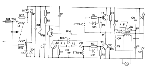
Fig. 1 shows the circuit diagram of an electronic
converter for 12 V incandescent halogen lamps with a maximum
power consumption of 105 W. The individual components will
be explained below. The input of the circuit is protected by
the fuse S11 and the thermal switch TS1 against excessive
currents and excessive temperature. This is followed by a
differential interference suppression filter, comprising the
X capacitor C12 and the double choke L1. One of each of the
two windings of the double choke L1 is connected serially
with one each of the two supply leads of the input and is
damped each with a parallel resistor R12, R13. This is
followed by a mains rectifier, comprising the diodes Dl-D4
in a bridge circuit, whose output has a parallel-connected
filter capacitor C14 and a varistor VAR as overvoltage
protection.
This is followed by a free-running current-
feedback inverter in a half-bridge circuit. Its function is
extensively described in German Patent Application
P 44 16 401. Therefore only the individual functional groups
and components will be described below. Its key part is a
free-running, current-feedback half-bridge converter,
essentially comprising the two switching transistors T1, T2-
to each of which one return diode D7, D8 is connected
parallel; the two bridge capacitors C8, C9, each with one
parallel-connected diode D9, D10; the power transformer TR1,
-15-
CA 02190150 2003-09-11
27813-58
whose secondary winding is connected to the positive pole of
the mains rectifier via the radio interference suppression
capacitors C6, C7 and to which a 12 V incandescent halogen
lamp is connected; and a control transmitter STR1-A through
STR1-C, which furnishes the control signals for the bridge
transistors T1, T2, which signals are supplied, each via a
trigger circuit comprising the resistors R2, R4 and R3, R5
and the diodes D15 and D16, respectively, to the base
terminals of the bridge transistors Tl and T2. The half-
bridge converter is started by means of a conventional
trigger generator, which essentially comprises the resistors
R1, R7, the charge capacitor C2, and the diac DIAC1. The
transistor T4, connected parallel to the charge capacitor
C2, whose base is connected via the resistor R14 to the base
of the half-bridge transistor T2, prevents the occurrence of
undesired trigger pulses while the half-bridge converter is
oscillating. This characteristic is already disclosed in
German Patent Application P 44 16 401. A protection circuit
known per se, substantially comprising the transistor T3,
the capacitors C3, C5, the diode D11 and the resistors R6,
R8 and R11, protects the bridge transistors T1, T2 against
secondary-side overload. The radio interference suppression
circuit comprises an additional winding ZW on the power
transformer TR1 and a metal face F. The additional winding
ZW and the primary winding of the power transformer TR1 have
opposite winding directions and each comprise 73 windings.
They are connected to one another at the base point FP. The
free end of the additional winding ZW is contacted to the
metal face F. In this way, the potential changes of the
center point M between the two bridge transistors Tl, T2 are
transmitted in phase opposition to the metal face F. The
components used are listed in Table 1.
-16-
CA 02190150 2003-09-11
27813-58
Fig. 2 shows the layout of the printed circuit
board, produced and equipped in accordance with Fig, 1. In a
known manner, radio interference is dependent to a high
degree on parasitic capacitances and inductances and
consequently on the components used, their three-dimensional
arrangement, and their electrical connections to one
another. The metal face F is therefore carefully adapted to
this layout. The production of the metal face F is effected
upon etching of the printed circuit board directly out of
the copper coating. Thus there are neither additional
production expenses nor additional material costs. This is
accordingly an especially economical form of the
interference suppression circuit according to the invention.
In Figs. 3a-3b, the quasi-peak (QP) interference
spectra of the electric circuit of Fig. 2 are shown,
measured in accordance with the specifications of CISPR 15.
During the measurement, a 100 W incandescent halogen lamp is
operated with supply leads, approximately 2 m long, that are
connected to the additional winding ZW of the power
transformer TR1. It can clearly be seen that the measured
values over the entire measurement range (20 kHz to 30 MHz)
are at times considerably below the CISPR 15 limit value
line G shown. Fig. 3a shows the course of the QP measurement
signal as a function of the frequency in the range between
150 kHz and 30 MHz. Figs. 3b and 3c correspondingly show the
ranges between 50 kHz and 1.4 MHz, and between 20 kHz and
160 kHz, respectively. In the last illustration, the
fundamental frequency of the inverter at approximately
32 kHz and the two subsequent harmonics at twice and four
times the fundamental frequency, respectively, are readily
visible.
Fig. 4 shows the basic circuit diagram of an
electronic converter with a controlled serial additional
-17-
CA 02190150 2003-09-11
27813-58
source. The circuit comprises the following components: feed
transformer ES, mains rectifier GR, trigger generator TG,
and self-excited current-feedback half-bridge converter HB.
The feed transformer ES comprises a primary winding WE1 and
two secondary windings WE2 and WE3 that are connected
serially to the mains supply leads N. The half-bridge
converter HB substantially comprises the two bridge
transistors T1 and T2, the two bridge capacitors C2 and C3,
the power transformer TR1, and the control transmitter RK-a
through RK-c. The rectifier GR and trigger generator TG
correspond to those of Fig. 1 and are merely shown as
function blocks for the sake of simplicity. The secondary
windings WE2 and WE3 are connected by their first ends C and
D, respectively, to the mains N and by their second ends c
and d to the inputs G1 and G2, respectively, of the mains
rectifier GR. The primary winding WE1 is connected by its
first end to the input E2 of the half-bridge converter HB.
The second end is connected via the impedance Z to the
center point M of the two half-bridge transistors T1 and T2.
In this way, a synchronizing current that is proportional to
the interference potential of the center point M flows in
the primary winding WE1 and in each of the secondary
windings WE2 and WE3 :induces a phase-opposed compensation
voltage. The amplitude of the compensation voltage is
adapted to the interference potential by means of the
impedance Z in such a way that the two voltages compensate
for one another, thus averting the occurrence of common-mode
noise. In a variant, the feed transformer ES is connected
not in the mains supply leads N but rather between the mains
rectifier GR and the :input of the half-bridge converter HB.
In that case, the terminals C, D and c, d of the two
secondary windings of the feed transformer ES are connected
to the two outputs G3, G4 of the mains rectifier GR and the
inputs E1 and E2 of the half-bridge converter HB,
-18-
CA 02190150 2003-09-11
27813-58
respectively. The terminals of the primary winding remain
unchanged.
Fig. 5 shows a further exemplary embodiment of an
open-loop controlled :radio interference suppression circuit,
which has a push-pull end stage GE and a metal face F
connected to it as a parallel-connected additional source.
The push-pull end stage substantially comprises the two
complementary transistors T5 and T6 and one basic connection
each by means of a resistor R15 and a diode D16. The metal
face F is contacted to the center point M2 between the two
complementary transistors T5 and T6. The open-loop control
circuit comprises the inverter stage I and the driver stage
T and it triggers the push-pull end stage. This radio
interference suppression circuit can be built into the
electronic converter of Fig. 1, for instance. In that case,
the additional winding ZW can be omitted. The control input
S is connected to the center point M of the bridge
transistors, and the + and - terminals of the voltage supply
of the push-pull end stage GE are connected respectively to
the outputs G3 and G4 of the mains rectifier GR.
Fig. 6 shows a further exemplary embodiment of a
radio interference suppression circuit, which has a push-
pull end stage GE and a metal face F connected to it, as a
parallel-connected additional source. Unlike Fig. 5, here
the circuit is designed as a closed-loop control circuit. To
that end, the driver stage T is supplied from the secondary
winding WS3 of a sensor transformer SE. The primary side of
the sensor transformer SE has two windings WS1 and WS2,
whose winding direction is adapted to the secondary winding
WS3 in such a way that only primary-side common-mode noise
generates a secondary-side signal. To that end, the first
ends A and B of the two primary windings WS1 and WS2 are
connected to the two mains supply leads N or alternatively
-18a-
CA 02190150 2003-09-11
27813-58
to the two outputs G3 and G4, respectively, of the mains
rectifier GR. The two other ends a and b of the secondary
windings are contacted to the inputs G1, G2 of the mains
rectifier GR, or alternatively to the inputs E1, E2 of the
half-bridge converter HB.
Fig. 7, finally, shows an exemplary embodiment of
a closed-loop controlled radio interference suppression
circuit, in which two secondary windings of a transformer
are used as serially connected additional sources. This
circuit has both a sensor transformer SE as in Fig. 6 and a
feed transformer ES as in Fig. 4. The terminals a and c, on
the one hand, and b and d, on the other, of the windings,
serially connected into the supply leads, of the two
transformers are connected to one another. The secondary
winding WS3 of the sensor transformer SE is connected via
the driver stage T to the primary winding WEl of the feed
transformer ES. The driver stage is formed by an operational
amplifier, whose inputs are connected to one another via the
resistor RT. The circuit may for instance precede or follow
the mains rectifier GR. In the first case, in Fig. 4, the
interfaces C, D and c, d are disconnected, and instead of
the feed transformer ES, the terminals A, B and C, D of the
circuit of Fig. 7 are connected to the mains supply leads N
or to the inputs G1, G2 of the mains rectifier GR. In the
second case, in Fig. 4 the connections between G3, E1 and
G4, E2 are disconnected, and instead the terminals A, B and
C, D of the circuit of Fig. 7 are connected to the outputs
G3, G4 of the mains rectifier GR or to the inputs E1, E2 of
the half-bridge converter. The feed transformer ES is
removed from the circuit, and the interfaces C, c and D, d
are connected to one another. The dimensioning of the
closed-loop control circuit can be seen from Table 1.
-18b-
CA 02190150 2003-09-11
27813-58
The invention is not limited to the exemplary
embodiments described. In particular, individual
characteristics of different exemplary embodiments may also
be combined with one another. Moreover, the inverters
mentioned may also be in the form of a full-bridge circuit
and/or the decoupling circuit may be a resonant circuit for
igniting and operating discharge lamps, without in principle
requiring any change in the interference suppression
circuit, or any loss of its advantageous effect. Finally, it
is also possible for the exemplary embodiments of radio
interference suppression circuits described to be installed,
without fundamental changes, in other embodiments of a
switching power supply, such as in choke converters
(downward, upward, upward-downward controllers, inverters),
flyback converters, and flow converters. In addition,
identical or different forms of switching power supplies may
also be combined with one another in the manner of a cascade
circuit, with each individual switching power supply having
its own radio interference suppression circuit.
-18c-
CA 02190150 2003-09-11
SI1 T 1A
Rl 16s kS2
R2, R3 . 3,3 S2
R4, RS 100 S2
R6 s60 S2
R7 165 kS2
Rs s 1 kS2
R9 330 kS2
R11 240 kSZ
R12,R13 10 kS2
R14 1 kS2
C2 10 nF; 250 V
C3 47 F; 6,3 V
Cs 6,7 nF; 400 V
C6,C7 470 F; 2 kV
CS,C9 88 nF; 400 V
C l2 220 nF; 2sOV
C 14 1 s0 nF; 400 V
D 1-D4 1 N4007
D7-DIO ' 1N4937
DI 1, D14, Dls LL4148
-
DIACI NEC, 32V
L 1 BVL32
STR1-A-STR1-C EF16 4.5/15.5/1sS windin
TRI R26 73/73/8 windings
T1, T2 SGS F343
T3,T4 BC8sOC
VAR S 10 K250
Table 1: Component list for the circuit of Fig. 1
-19-
CA 02190150 2003-09-11
WS l, WS2 2 windin s
WS3 50 windin s
RT 47 kS2
T AD 844
WE1 5 winain s
WE2, WE3 50 .windings
Table 2: Component list for the circuit of Fig. 7
-20-