Note: Descriptions are shown in the official language in which they were submitted.
WO 95/33208 ~ ~ ~ ~~ ~ ~ ~ PCTIUS95I06896
1
DIGITAL FORCE BALANCED INSTRUMENT
BACKGROUND OF THE INVENTION
1. ~'ie~d o~ the Inven+;~n
The present invention relates to instruments. More
precisely, the present invention relates to a digital
force balanced instrument that incorporates a directly
digital electrostatic forcer with servo loop plates
charged by a digital feedback loop.
2. Prior z,rt and Related Tnformat~on
Precise instruments such as accelerometers are used
in a variety of applications, such as in measuring the
acceleration or deceleration of a ship, missile, or
airplane. A conventional accelerometer uses a pendulum
type transducer in which acceleration is detected by
noting the displacement of the pendulum. A force is
applied to the pendulum, generally by an electromagnetic
field, in order to force the pendulum back to its initial,
pre-displacement position. By detecting the current
required to generate the electromagnetic field, one could
determine the acceleration. A more recent accelerometer
design relies on a movable, silicon electrode that is
positioned between two fixed electrodes while cantilevered
to a silicon base. The movable electrode is spaced apart
from two fixed electrodes. The entire structure is
sandwiched within a glass shell and electrically connected
to monitoring circuitry.
Within any system using inertial instruments such as
accelerometers, there is a computer that operates on the
data provided by the inertial sensor or accelerometer. It
is highly desirable for the inertial instruments to output
digital data directly to the computer, thereby eliminating
the need for complicated quantizer circuitry. Indeed, it
is much easier to transmit and operate on a digital
representation of a signal rather than on the older,
analog form.
CA 02190608 1999-O1-04
2
There have been attempts to build a digital output
accelerometer using electrostatic forcing. These
generally fall into two classes: charge controlled (see
U.S. Patent No. 5,142,921), and voltage controlled. The
present invention instrument is voltage controlled, meaning
that voltages are applied to the electrostatic forcing
plates to produce a force. Also related is United States
Patent No. 5,503,285 entitled Electrostatically Force
Balanced Silicon Accelerometer disclosing processes for
1.0 fabricating electrostatic forcers.
Also, U.S. Patent No. 5,142,921 to Stewart et al.
discloses a force balanced instrument with electrostatic
charge control. More precisely, the invention is directed
to a force balanced instrument employing a pendulous mass
having combined electrostatic pickoff and forcing plates
on opposite sides thereof. The operative principle in
the instrument dictates that the resulting force is
proportional to the square of the applied voltage.
This principle, known as the square law, necessitates
20 use of a microprocessor to take the square root of the
voltage in order to obtain the force. This is a
relatively complicated and expensive method, aad is
inherently non-linear. Potential error sources include
numeric round-off in the square root routine or look-up
tables of any software used. Also, any rounding or time
constant associated with the application of a voltage
pulse exhibits different force weight with different pulse
heights.
Another method of linear force balance is achieved by
30 controlling the duty cycle so that the difference in
duration between each of the parts of a full cycle is a
linear measurement of acceleration. One drawback to this
approach is that it tends to use maximum allowable voltage
at all times, such that there is a tendency to suddenly
move the proofmass in opposite directions. This is
commonly referred to as °pinging.~~
62948-224
CA 02190608 1999-O1-04
3
For good bias stability, the application of a large
force to the proofmass is to be avoided when only a small
force is needed to return the proofmass to the null
position. With a large force applied to the proofmass,
the electrostatic negative spring rate problems increase,
and temperature-dependant non-linearities become worse.
One approach to overcoming such pinging problems is to use
a high speed clock for fine resolution; however, for many
applications, that approach causes an unacceptable
1o increase in the power demand.
Previous voltage-biased, linearized force methods
exhibit very large negative spring rates as a result of
the electrostatic field from the bias voltage which is
always present.
Accordingly, a need presently exists for a digital
force balanced instrument that provides an output digital
code that is directly linear with input force. This would
eliminate the square law problems.
62948-224
PCTIUS95106896
W O 95/33208
2/GD~~~
4
In view of the foregoing, it is therefore an object
of the present invention digital instrument to provide an
output digital code that is directly linear with input
force. It is another object of the present invention to
not require square or square-rooting in order to obtain
force balancing data. It is yet another object of the
present invention to provide voltage driven plates, with
to negligible sensitivity to stray capacitance. It is still
yet another object of the present invention to not require
an op amp or analog stages in the force balancing output.
It is another object of the present invention to employ
simplified circuitry; i.e., quantization performed by an
A/D converter available as one chip. It is also an object
that the present invention instrument should have low
applied force near zero g, which should result in good
bias performance at low g inputs.
To achieve the foregoing objects, the present
invention in a preferred embodiment provides a digital
force balanced instrument, an accelerometer in this
instance, that- comprises a semiconductor proofmass
electrode generating an analog output signal. The
proofmass is surrounded by a semiconductor substrate base.
A hinge supporting the proofmass on the surrounding
substrate holds the proofmass in a cantilevered position.
Gaps are located between the proofmass and surrounding
substrate.
A network of electrostatic plates is disposed in a
symmetrical array on the surrounding substrate, on
opposite sides of the proofmass. Ideally, the plates are
arranged about the dynamic centroid of the proofmass
electrode to distribute the electrostatic charge at
strategic locations.
A pickoff voltage oscillator is connected to the
electrostatic plates, which induces a signal in the
proofmass. This signal is amplified by an amplifier
CA 02190608 1999-08-10
connected to the proofmass. A demodulator connected to the
amplifier demodulates the analog output signal, and feeds the
output to an integrator, which smoothes the analog output
signal, and outputs a restore signal having an amplitude
5 indicative of the force required to prevent displacement of the
proofmass. An analog to digital converter receives the restore
signal and provides a digital output signal representative of
the amplitude of the restore signal, which is then held in a
plurality of latches corresponding to the electrostatic plates.
Each latch selectively provides an output control signal in
accordance with the digital output signal to FET switches
connected to each corresponding electrostatic plate. In turn,
the FET switches activate or ground the corresponding
electrostatic field that restores the proofmass to an initial
position
The digital output signal of the present invention is
therefore linear with the input force. Hence, a square law
solving microprocessor is not needed, and the associated expense
and complications are eliminated.
In accordance with the present invention, there is provided
a digital force balanced instrument for detecting an outside
force comprising: a proofmass; a substrate; two electrodes
disposed on the substrate straddling the proofmass, wherein each
electrode is divided into a plurality of cells wherein each cell
has a least significant bit of area; a circuit obtaining a
digital signal of a value representing a velocity of the
proofmass under the outside force during each of equal units of
time, wherein the outside force moves the proofmass from a null
position, and wherein the circuit also generates a constant
voltage signal; whereby in accordance with the value of the
digital signal, the circuit applies the constant voltage signal
to selected cells to energize only such number of cells as is
necessary to generate a force from an electric field resulting
from the application of the constant voltage signal to the cells
CA 02190608 1999-08-10
5a
in order to urge the proofmass to return to the null position.
In accordance with the present invention, there is further
provided a method of applying force to a proofmass cantilevered
on a substrate of a digital force balanced instrument: providing
the proofmass, wherein the proofmass includes a null position
and a force-induced position on either side of the null
position, wherein the proofmass is responsive to an outside
force which moves the proofmass from the null position to one of
the force-induced positions; providing one electrode on each
side of the proofmass, each of said electrodes having a
plurality of electrically separate cells, wherein each cell has
an area value equal to a least significant bit; during each of
equal units of time, obtaining a digital signal having a value
representing the change in velocity of the proofmass in response
to the outside force; generating a constant voltage signal; in
accordance with the value of the digital signal, applying the
constant voltage signal to selected ones of said electrode cells
to energize only such numbers S of said cells as is necessary,
using force from an electric field resulting from the
application of the constant voltage signal to such cells, to
urge the proofmass from the force-induced position to return to
the null position.
In accordance with the present invention, there is further
provided a digital force balanced instrument for detecting an
outside force comprising: a substrate; a proofmass electrode for
providing an output analog signal; a hinge connecting the
proffmass to said substrate in a cantilever configuration; a
plurality of electrostatic plates selectively operating in
unison to form one or more functional cells disposed on either
side of the proofmass electrode; control switches connected to
each of said plates; a pick-off oscillator connected to said
plates; an integrator responsive to the output analog signal to
provide an output restore signal indicative of displacement of
the proofmass; a cascading voltage level detector responsive to
CA 02190608 1999-08-10
5b
the output restore signal, to provide an output digital signal
containing data proportional to the output restore signal; and a
latch corresponding to one plate, receiving the output digital
signal from the cascading voltage level detector, wherein the
latch activates the respective control switch.
In accordance with the present invention, there is further
provided a digital force balanced instrument for detecting an
outside force comprising: a proofmass to provide an analog
output signal, a substrate surrounding the proofmass; a hinge
supporting said proofmass on said surrounding substrate; a
plurality of electrostatic plates selectively operating in
unison to form one or more functional cells disposed on the
surrounding substrate; a pickoff voltage oscillator connected to
electrostatic plates; an integrator receiving the analog output
signal and providing a restore signal having an amplitude
indicative of a displacement of the proofmass; an analog to
digital converter receiving the restore signal and providing a
digital output signal representative of the amplitude of the
restore signal; a plurality of latches corresponding to the
electrostatic plates, said latches responding to the digital
output signal to selectively provide an output control signal in
accordance with the digital output signal; and control switches
connected to each corresponding electrostatic plate and each
respective latch, wherein the output control signal selectively
activates the control switches; whereby the electrostatic plates
are individually activated and generate an electrostatic field
that restores the proofmass to an initial position.
In accordance with the present invention, there is further
provided a digital force balanced instrument for detecting an
outside force comprising: a semiconductor proofmass electrode,
providing an analog output signal; a surrounding semiconductor
substrate; a hinge supporting the proofmass on the surrounding
substrate in a cantilevered position; gaps located between the
proofmass and surrounding substrate; a plurality of
CA 02190608 1999-08-10
5c
electrostatic plates disposed in a grid pattern on the
surrounding substrate, on opposite sides of the proofmass; a
pickoff voltage oscillator connected to the electrostatic
plates; an amplifier connected to the proofmass for amplifying
the analog output signal; a demodulator connected to the
amplifier for demodulating the analog output signal; an
integrator receiving the analog output signal from the
demodulator, and providing a restore signal having an amplitude
indicative of a displacement of the proofmass; an analog to
digital converter receiving the restore signal and providing a
digital output signal representative of the amplitude of the
restore signal; a plurality of latches corresponding to the
electrostatic plates, receiving the digital output signal,
wherein each latch selectively provides an output control signal
in accordance with the digital output signal; FET switches
connected to each corresponding electrostatic plate and to each
corresponding latch, wherein the output control signal
selectively activates the FET switches; whereby the
electrostatic plates are individually activated and generate a
voltage driven electrostatic field that restores the proofmass
to an initial position.
In accordance with the present invention, there is further
provided a digital force balanced instrument for detecting an
outside force comprising: a proofmass, including a centroid, to
provide an analog output signal; a substrate surrounding the
proofmass; a hinge supporting said proofmass on said surrounding
substrate; electrostatic plates disposed on the surrounding
substrate at a predetermined distance from the centroid; a
pickoff voltage oscillator connected to the electrostatic
plates; an integrator receiving the analog output signal and
providing a restore signal having an amplitude indicative of a
displacement of the proofmass; an analog to digital converter
receiving the restore signal and providing a digital output
signal representative of the amplitude of the restore signal; a
CA 02190608 1999-08-10
5d
plurality of latches corresponding to the electrostatic plates,
said latches responding to the digital output signal to
selectively provide an output control signal in accordance with
the digital output signal, wherein a quantity of activate
plates increases proportionally to a value contained in the
digital output signal; and control switches connected to each
corresponding electrostatic plate and each respective latch,
wherein the output control signal selectively activates the
control switches; whereby the electrostatic plates are
individually activated and generate an electrostatic field that
restores the proofmass to an initial position.
WO 95/33208 PCTIUS95106896
219o~D~
6
BRT_EF DESCRTPTT_ON OF THE DRAWTNGS
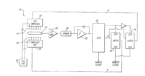
Fig. 1 provides a general schematic overview of a
preferred embodiment of the present invention, showing the
accelerometer and associated feedback loop circuitry.
T
Figs. 2 and 2A provide a plan view and a magnified
plan view, respectively, of a preferred embodiment
arrangement of the electrostatic plates disposed on the
,10 surrounding substrate.
Fig. 3 is a plan view of an alternative embodiment of
the present invention with the electrostatic plates.
Fig. 4 is a schematic of a pattern defining cells and
arrays.
Fig. 5 shows details of the conductors and enlarges
a part of Fig. 2.
R'O 95!33208 ~ PCT1U595/06896
7
DETATrED DESCI2TPmTpN OF THE INVEN'TTnN
The following specification describes a digital force
. balanced instrument. In the description, specific
materials and configurations are set forth in order to
provide a more complete understanding of the present
invention. But it is understood by those skilled in the
art that the present invention can be practiced without
those specific details. In some instances, well-known
elements are not described precisely so as not to obscure
the invention.
Generally, the present invention is directed to a
digital force balanced instrument with a feedback loop.
The underlying principle behind the present invention
instrument, as is known in the art, is described as
follows. The force F acting on a proofmass due to a
voltage V on a forcing electrode (proofmass potential = 0)
is: F = ~~° A ~ where d is the a between the
as g P proofmass
and the electrode. Also, A represents the charged area on
the electrode; e° is the permittivity of free space; ander
is the relative permittivity of the gap between the
forcing electrode and the proofmass.
Fig. 1 is a schematic overview of a preferred
embodiment of the present invention. The preferred
embodiment of the present invention instrument is directed
to an accelerometer 10 that employs multiple electrodes
14, 16 on either side of the proofmass 12, wherein each
electrode 14, 16 is divided into cells of binarily
weighted areas. As seen here, once an inertial force is
encountered by the accelerometer 10, the proofmass 12
moves and produces a change in the electric field
generated by the plates of the electrodes 14, 16.
Fig. 2 is a plan view of a preferred embodiment
instrument having plates 40 disposed on the substrate
surfaces opposing (e. g., above and below) the proofmass
PCTIU595I06896
WO 95133208
2190~0~
42. In an alternative embodiment (not shown), the plates
may be disposed on the proofmass as well. A constant
voltage is switched onto each plate 40 in response to a
binary code as required to generate a force that will most
closely approximate the input force. Since voltage V is
a constant, the accelerometer 10 is operated at one point
on the square-law curve with a constant force per unit
area. By successively switching unit areas defined by the
number of activated plates, when grouped together called
cells, off and on in multiples of two at a constant
voltage, sufficient numbers of cells are energized and
generate an electric field that returns the proofmass 12
to the null position.
It is useful now to define several terms. A "cell,'°
as explained above, is a unit area of an electrode
disposed on a substrate or, in the alternative embodiment,
the proofmass. When a constant voltage is applied to one
of such unit areas, the cell creates a least significant
bit of force to the proofmass.
Fig. 4 shows an electrode layout with a smaller
arrangement of cells to facilitate explanation.
Specifically, Fig. 4 shows one cell or unit area #1, which
is a one-bit array. That first square cell ,~1 has an area
of one least significant bit, and is centered on both the
x and y axes. This is a one bit cell ~1.
Two sets of cells having the same number of cells in
.each set form an "array" of cells. The combined arrays of
cells on the substrate form a "pattern" of cells on the
entire substrate.
In Fig. 4, the two adjacent cells #2 form a two-bit
array. These two cells ~2 are centered on the x axis and
are symmetrical to the left and right oP the first cell
;~1. Each of the two cells ~2 has a one bit area value,
such that when both cells ,~2 are energized, they represent
the two bit value.
Similar results are obtained with a four bit array,
which includes four cells ~3 each of one bit area value.
WO 95133208 ~ PCT/US95106896
9
The four bit array is comprised of two cells ,~3 to the
left of the left second cell ,~2, and two cells ~3 to the
right of the right second cell ,~2. Together these four,
one-bit cells ~3 represent a four bit value array.
In contrast, as best seen in Figs. 2 and 2A, the one
bit cell has four sections #4, each of which is about one-
quarter bit in value. So in the more complex embodiment
of Figs. 2 and 2A, four one-quarter bit sections #4 form
the one bit cell. The next sections are for the two-bit
value array each includes four, one-quarter-bit sections
#8. The next sections are for the four-bit value ,~16,
comprising sixteen one-quarter bit section #16. The next
sections are for the eight-bit value ;~32. The next
sections are for the sixteen-bit value ,~64.
A "set" of cells includes a selected number 'S" of
cells which are to be energized together during any given
time interval. In Fig. 4, the number S of cells to be
energized is "one" for one bit since the one cell ,~1 is
of
one bit value. As shown in Fig. 4, for a two bit value,
only the two ~'2 cells are energized such that S is two.
Similarly, for a four bit value, only the four ~'3 cells
shown in Fig. 4 are energized, and the number S is thus
four. Thus, successive sets have binary multiples of
value; e.g., 1, 2, 4, 8, 16, 32, 64, etc.
Figs. 2 and 2A, wherein the latter is a magnified
view of the former, show a more complicated array. S is
one for the one bit cell, but the one bit cell has four
sections ,~4. For the two bit value, the next two outer
cells are energized such that S is two, but each of these
cells has four sections #8 so that eight sections are
energized.
In each case, the cells of one set are electrically
insulated from the cells of another set. One such set is
on each side of the centroid of the electrode. This is
shown in Fig. 5, which is an enlarge, partial view of Fig.
2. The one-bit cell ,~1 has been omitted from the drawing
for clarity. The interconnection, or intra-cell
W0 95133208 PCT/US95/06896
l0 2I901o08
conductors 44, are shown. As explained earlier, the four-
bit array comprised of four one-bit cells ~'3 are
interconnected. A bus 46 and a primary conductor 48 are
the main paths for signal input/output for each set of '
cells. Within a set, there are additional inter-set
conductors that extend from the cell on one side of the y-
axis to the cell on the other side of the y-axis. Also,
the intra-cell conductors 44 electrically interconnecting
the sections of one cell. Accordingly, it should be clear
the sequence at which the exemplary embodiment energizes
cells in order to force the proofmass 12 to its null
position after being displaced.
In Fig. 5, it is more important to note that the
areas and locations of all of the conductors relative to
the hinge must be taken into consideration when
calculating the total area of a cell. In particular,
voltage appears on all of these conductors, and has an
effect on the proofmass. The magnitude of the effect
depends on the distance of the conductor from the hinge,
and on the area of that conductor.
To enable the areas of the cells to be trimmed -- for
purposes of assuring cell and conductor symmetry around
both the x and y axes, for example -- two types of
additional conductors are provided. First, °'trim°'
conductor are shown in Fig. 2, and are connected to
various cells. The trim conductors are at a particular
location. Next, lead ends are shown, but these are not
trimmed.
By trimming the trim conductors, and selectively
locating the lead ends, and selectively locating the
cells, there is no torsional twist around the y axis when
voltage is applied to the electrodes, and each of the
opposite electrodes applies the same force on the
proofmass from oppositely disposed locations.
Finally, in Fig. 2 there is a dashed line shown
opposite to the hinge. The dashed line denotes the end of
the proofmass such that the inter-set conductor shown in
W0 95133208 PCT/US95/06896
11
solid line does not have any force effect on the
proofmass.
The sets which form a particular array are positioned
on the substrate symmetrically relative to an orthogonal
axis system (x and y axes), with one set on one side of
the y axis, and the other set on the other side of the y
axis, and wherein each set is symmetrical relative to the
x axis.
There are several factors that influence the
1o particular layout of the cells and sections. The factors
include: (1) efficient use of the wafer area; and (2)
having the torque applied by the electrode to the
proofmass be neutral around each of the x and y axes.
This is achieved by disposing all sections symmetrically
about the x and y axes. In Fig. 2, for example, the four,
eight, and sixteen bit arrays have cells in a "C" or
reverse "C" shape for symmetry.
In the construction of the present invention
instrument shown in Figs. 2, 2A and 3, the electrode 14,
16 layout is composed of the individual cells of area
described above. This is done in order to maintain a
constant °'undercutting periphery" to "enclosed area"
ratio, which will be required to accurately
photolithographically pattern and etch metallization of
the electrodes. The electrode pattern has its area
centroid 18 located above the proofmass 12 center of mass
or center of percussion (as desired) of the proofmass and
is symmetrical about a pendulous axis. The power of
binary scaling of the electrode areas is very desirable
for direct interfacing to digital computer systems as
parallel binary bytes or words. The resolution of this
technique for long measurement times is not limited simply
to the number of bits of resolution of the electrodes,
since changes smaller than the least significant bit can
be represented by dithering between the different binary
codes in successive time periods. The loop is typically
updated at ten kHz.
WO 95133208 PCTIUS95106896
12
In a preferred embodiment, as seen in Figs. 2 and 2A,
the proofmass 12 and the opposing, surrounding substrate
are made from a semiconductor material. The electrode
surfaces are preferably made of Pyrex glass deposited with
thin-metal film.
Fig. 1 shows how a digital feedback loop using the
electrode plate pattern illustrated in Figs. 2, 2A and 3
would operate. The accelerometer 10 is shown
schematically with six electrodes 14, 16 on each side of
the proofmass, representing the binary ratioed electrode
areas. For ease of explanation, six plates are shown.
These plates 16 are switched to ground or to a constant
reference voltage by FET switches 22, 24 in response to a
digital code provided by the feedback loop. There can be
fewer or more than the six plates shown. The issue as to
how many cells to have is one of practicality. Factors
include: (a) the cell size, as such; (b) the substrate
area size, as such; (c) the desired line width of a
conductor (in microns); and (d) keeping an RC time
constant of one array the same as an RC time constant of
every other array.
A pickoff oscillator 20 supplies a time varying
reference signal to the electrode plates 16. The pickoff
oscillator 20 is used to provide an initial start position
(i.e., pickoff null position) of the proofmass 12. The
oscillator 20 is represented as a conventional oscillator,
typically operating at about 100 mV at 250 kHz. The
oscillator 20 is capacitively coupled into one or all of
the plates 16 on each side so as not to interfere with the
DC elements generated by the feedback loop, described
below.
The electric field generated by the pickoff signal on
electrode plates 16 induces an analog signal in the
proofmass 12. The signal is amplified by an AC amplifier
26, known in the art.
A phase sensitive demodulator 28 removes a carrier
portion of the analog signal originating from the pickoff
W0 95/33208 ~' PCTlUS95/06896
13
oscillator 20, and recovers the proofmass 12 position. At
this stage, the signal may be optionally rectified. The
output signal of the demodulator 28 is then averaged
through an integrator 30 with any required loop stability
compensation network.
Next, an output signal from the integrator 30 is
digitized by an A/D convertor 32 having a built-in sample
and hold capability. The A/D convertor 32 operates as a
cascading voltage level detector thereby sampling the
input analog signal and outputting a 6-bit word indicative
of the input signal.
The quantization at the end of each update of the A/D
convertor 32 would be output to the system. A stable
clock-derived signal controls the sample times of the A/D
convertor 32, typically at a rate of tens of kilohertz.
The output signal from the A/D convertor 32 is
latched by one of two latches 34, 36 depending on the sign
bit, and therefore either the top or bottom set of
accelerometer plates 16 respectively, are responding to
the digital code. The other latch is cleared and the
accelerometer plates 16 are grounded and provide no force.
Thus, the digital code having the sign bit resulting from
each cycle is output to activate specific FET switches 22,
24, that in turn activate the electrode plates 16. Once
a constant voltage is applied to the energized electrode
plates 14, 16, the electrostatic field generated thereon
restore the proofmass 12 to its initial position.
To measure force, the output signal from the A/D
convertor 32 can be sent to an optional microprocessor
(not shown) to convert the digital code to a numeric
approximation of the detected acceleration. In this
manner, the square law is not involved, and neither are
the associated inaccuracies and complications associated
with a square root subroutine and look-up tables.