Note: Descriptions are shown in the official language in which they were submitted.
2190$0q
FIELD OF THE INVENTION
The present invention relates to devices for measuring one or more
properties of a light signal. More particularly the invention relates to
devices for
wavelength and power demodulation based on the use of quantum well
electroabsorption photodiodes.
BACKGROUND OF THE INVENTION
The concept of an "optical multimeter", most simply defined as a
device that measures more than one aspect of an input light signal, has
received
increasing attention in the last few years. The possibility of having one
measurement device report on the power, wavelength, polarization and the like
is extremely attractive, and in the future, such optical multimeters may
become
as basic to the photonics industry as the digital multimeter has become to the
electronics industry.
Recently, systems for wavelength measurement have been
proposed which make use of quantum well electroabsorption devices as
wavelength tunable filters or as wavelength tunable filtering detectors, as
disclosed in United States Patent No.5,469,265. Applying an electric field
across
the quantum well region of the photodiode results is a shift in the optical
absorption edge of the quantum well structure, in accordance with the quantum
confined Stark effect, so that the wavelength characteristics of these devices
may be tuned.
However, proposed systems to date have focussed on the
waveguide approach with input light signal being coupled into the thin
-1-
2i90~04
waveguide region of the photodiode and travelling parallel to the quantum well
in the plane of the well layers. This approach is advantageous in many
applications but suffers from two problems which make it undesirable for use
in
development of commercial optical multimeters. First, the waveguide approach
is polarization dependent. Specifically, the quantum confined Stark effect is
sensitive to whether or not the electric field is polarized parallel or
perpendicular
to the plane of the quantum wells, resulting in distinct TE and TM behavior.
Secondly, optical alignment of the input light signal with the
quantum wells is problematic. The cross sectional dimensions semiconductor
waveguides are typically of the order of a few microns, so that optical
coupling
of light into the waveguide is a very challenging alignment problem requiring
extremely fine positioning and good stability of the input light signal with
respect
to the waveguide.
In order to facilitate the development of optical multimeters based
on quantum well electroabsorption devices, alternative device architectures
must
be identified which offer the potential for simple, flexible and low cost
measurement of more than one characteristic of a light signal, while avoiding
problems polarization sensitivity and optical alignment of the input light
signal.
SUMMARY OF THE INVENTION
It is an object of the present invention to provide a device for
measuring one or more characteristics of a light signal.
It is also an object of the present invention to provide a device for
measuring one or more characteristics of a light signal which does not require
-2-
CA 02190804 2001-11-20
precision alignment between the detector and the input light signal and which
is
not limited by light polarization restrictions.
The present invention provides a device for measuring properties
of an input light signal. The device includes a light signal detection means
comprising a quantum well photodiode having at least one planar quantum well
and an absorption edge with the light signal detection means having an output.
Included is a reference detection means having an output forms part of the
device and means for impinging a portion of an input light signal on the
reference detection means and another portion of the input light signal on the
light signal detection means at an effective angle with respect to the planar
quantum well. The device includes a signal processing means with the outputs
of the light signal detection means and reference detection means being
connected to the signal processing means which combines the outputs in a
preselected manner. The signal processing means has an output signal
indicative of the combined outputs. The device includes a biasing means for
biasing the quantum well photodiode for tuning the absorption edge of the
quantum well photodiode. In this aspect of the invention the effective angle
is
substantially perpendicular to the plane of the quantum well.
In another aspect of the invention there is provided a device for
c'0 measuring properties of a Bight signal. The device comprises a filtering
detector
which comprises a quantum well photodiode having an absorption edge, at least
one substantially planar quantum well and an output. The device includes a
reference photodetector having an output and a means for impinging a portion
of an input light signal on the reference photodetector and another portion of
the
-3-
CA 02190804 2001-11-20
input light signal on the quantum well photodiode at an angle substantially
perpendicular to the planar quantum well. The device includes a signal
processing means with the outputs of the filtering detector and the reference
photodetector being connected to the signal processing means which combines
the outputs in a preselected manner. The signal processing means has an
output signal indicative of the combined outputs. The device includes biasing
means for biasing the quantum well photodiode for tuning the absorption edge
of the quantum well photodiode.
BRIEF DESCRIPTION OF THE DRAWINGS
The method and devices for wavelength and power demodulation
using quantum well electroabsorption filtering detectors forming the subject
invention will now be described, by example only, reference being had to the
accompanying drawings, in which:
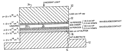
Figure 1 is a cross sectional view of a multiple quantum well
photodiode forming part of a quantum well electroabsorption detector according
to the present invention;
Figure 2 is a detailed view of the undoped sandwich layer of Figure
1;
Figure 3 is a block diagram of a divider based system which makes
use of a quantum well electroabsorption filtering detector to measure the
wavelength of an optical signal;
Figure 4 is a block diagram of a comparator based system which
uses a quantum well electroabsorption filtering detector to measure the
?5 wavelength and power of an optical signal;
-4-
2?9004
Figure 5 is a block diagram of an active wavelength demodulation
system using synchronous detection constructed in accordance with the present
invention for which experimental results are presented in Figures 7 to 10;
Figure 6 is a system state diagram illustrating how the system of
Figure 5 tracks the wavelength of an input light signal;
Figure 7 shows the open circuit wavelength response showing
output voltage of the divider versus wavelength (with the different bias
voltages
indicated in the legend) for the system of Figure 5 using the QW photodiode
shown in Figures 1 and 2, temperature controlled to 30.05°C;
Figure 8 shows the wavelength response, system voltage output
versus wavelength for the filtering detector of Figure 5 operating in closed
loop
(tracking) mode with a ratio lock point of 1.002 V and an average measurement
resolution for this lock point of ~8.33 picometers;
Figure 9 is similar to Figure 8 but with a ratio lock point of 2.012
V and for this lock point the measurement resolution is ~6.39 picometers;
Figure 10 is similar to Figures 8 and 9 and shows the closed loop
(tracking) wavelength response for various system lock points using
synchronous detection with the QW diode structure of Figure 1; and
Figure 11 shows an example of packaging a QW filtering detector
which is temperature controlled.
DETAILED DESCRIPTION OF THE INVENTION
The quantum well electroabsorption (QW EA) filtering detectors
constructed in accordance with the present invention make use of multiple (or
-5-
i
CA 02190804 2002-05-02
single) quantum well (QW) photodiodes, whose spectral response near the
absorption edge may be tunable utilizing the quantum confined Stark effect by
applying a variable reverse bias voltage across the photodiode. The principle
of this method of wavelength demodulation system is briefly discussed in
United
States Patent No. 5,469,265 issued November 21, 1995 to Measures et al .
Referring to Figure 1, a cross sectional view is shown of an
example quantum well photodiode at 10. Photodiode 10 is a layered
semiconductor structure comprising an n-doped indium phosphide (InP)
substrate 12 with an n-doped portion 14 on which a 500 nm of n-doped InP
buffer layer 16 is applied followed by a lower n-doped waveguide contact 20
comprising nineteen periods of 2.0 nm InGaAs118.0 nm InP layers. An upper p-
doped waveguide contact 22 comprises nineteen periods of 2.0 nm InGaAsI18.0
nm InP layers suitably doped. Interposed between the two waveguide contacts
20 and 22 is an undoped layer 24 to be discussed hereinafter. On top of the
upper waveguide contact 22 is located a p-doped layer 32 of InP. Thickness and
doping levels of the different layers is indicated in Figure 1 adjacent to the
associated layers. Similarly, the detailed view of Figure 2 gives the
thickness
and composition of the periods forming the undoped layer 24. Shown are three
different layers, lower and upper layers 26 and 30 and central layer 28
sandwiched between layers 26 and 30. Each layer comprises ten periods each
with different thicknesses and compositions as indicated. QW photodiode 10 has
a substantially planar upper surface 34 onto which the input light signal is
incident during use. This particular QW photodiode was produced by Lucent
-6-
219~8~4
Technologies-Bell Labs.
The center layer 28 of the undoped region is the portion of the
quantum well photodiode in which light absorption in the region of the
absorption
edge takes place. The materials and structure of this portion of the
photodiode
have been chosen to produce the tunable wavelength response of Figure 7,
discussed hereinafter. It will be understood by those skilled in the art that
the
semiconductor materials and structure of the QW photodiodes may be chosen
in various number of ways to produce photodiodes optimized for tunable
wavelength measurement over preselected wavelength ranges in addition to
other properties. A bias potential is shown applied to photodiode and this
bias
potential may be an externally applied potential or it may be part of a
feedback
loop of which the filtering detector forms a part, depending on the particular
application to be discussed hereinafter.
Using a QW EA photodiode in an orientation such as is shown in
Figure 1 with light incident substantially normal to the plane of the quantum
wells
offers two distinct advantages for optical multimeter (and other) applications
compared to the waveguide approach. First, because the electric field vector
of
light is always aligned parallel to the plane of the quantum wells, the device
is
independent of polarization effects. This is in contrast to waveguide devices
which are characterized by distinct TE and TM polarization responses
previously
discussed. A second advantage is that there is no need to couple light into a
very thin waveguide, The input light signal may be incident over a large
surface
area, in the photodiode shown in Figure 1, over the entire surface 34 of the
diode. Such an approach facilitates coupling of the input light signal to
areas
-7-
2 ~ 9~~~~.
which may be of diameter of hundreds of microns in size, dramatically
simplifying optical coupling to the QW EA device, and thus increasing
robustness of the system and decreasing packaging costs.
Unfortunately, only a small portion of the incident light is absorbed
by the filtering detector, since the absorbing region is only as long as the
width
of the quantum wells and because it is difficult to grow large numbers of
successive QW layers. For this reason, known QW EA modulators are generally
limited to waveguide structures where the light is incident "edge on",
parallel to
the plane of the quantum wells. However, when using these devices as filtering
detectors this low absorption means that the detector responses will be lower
in
amplitude than for standard detectors. It is in this manner that QW EA devices
may best be used for optical multimeter applications.
In practice, such QW photodiodes may be designed for various
applications, such as for operating in different wavelength ranges, light
intensity
sensitivities and wavelength resolution. For example, for measurement of very
low light intensities, multiple QW photodiodes are preferred while for
measurement of higher light intensities a single QW photodiode may be used.
Measurements requiring high resolution would preferably use a single QW
device, as multiple QW structures typically exhibit less steep wavelength
filter
slopes than do single QW structures. Therefore, the particular details of the
MQW device of Figures 1 and 2 are given as a non-limiting example only.
Figure 3 illustrates a block schematic diagram of a wavelength
demodulation system based on a quantum well electroabsorption (QWEA)
filtering detector at 40. The input optical signal passes through an optical
beam
_g_
splitter 82 with part of the signal input into a multiple quantum well
electroabsorption (MQW EA) tunable filtering detector 84 and the other part
into
a reference detector 86 which can be either a known photodiode detector or it
also may be a QW photodiode depending on the application. The output of
filtering detector 84 is amplified by means of an amplifier 88 and the output
of
reference detector 86 is input into an amplifier 90. The output from amplifier
90
serves as a measurement of the power of the input optical signal. The outputs
of amplifiers 88 and 90 are input into an analog divider circuit 96 where the
signals are ratioed. A ratiometric voltage signal, V~at~o, is obtained by
ratioing the
filtered output of filtering detector 84 and the unfiltered reference output
of
detector 86 to provide optical intensity self-referencing (immunity to input
power
fluctuations). This V~;o output signal is continuously compared with a
reference
voltage signal, V~ef, and the difference of V~at~o and V~e, is input into a
feedback
control circuit 100. The output voltage Vo~t of the feedback control circuit
100 is
used to bias the QW EA photodiode so that in closed loop operation the QW EA
photodiode is continuously wavelength tuned to maintain V~at~o equal to V~e,.
This
process will be discussed in more detail with respect to the detector of
Figure
5.
The feedback control in the system of Figure 3 may also be
disconnected, and the ratiometric signal from the divider used to determine
the
wavelength of an input optical signal, provided the spectral characteristics
of the
quantum well photodiode in detector 84 are well characterized. The use of the
quantum well photodiode in such an open loop version of the device of Figure
3 represents a significant advance over similar ratiometric wavelength
_g_
~ ~ '~~844
measurement techniques to date, since the absorption edge of the photodiode
may be tuned over a range of wavelengths, providing a greater wavelength
measurement range than would be possible using many non-tunable filters.
Furthermore, systems which rely on passive filters inherently suffer from a
trade-
off between measurement range and resolution, corresponding to low and high
filter slopes (with respect to wavelength) respectively. In contrast, the
tunable
filter based detectors forming the present invention allow high filter slopes
to be
maintained over an extended measurement range achieved by wavelength
tuning the filter.
Figure 4 is a block diagram of another embodiment for a QW EA
filtering detector based wavelength and power demodulation system 50.The
optical receiving portion of system 50 comprises a QW EA filtering detector 54
and a reference detector 52, each of which receives a portion of the input
optical
signal. Reference detector 52 is only partially absorbing, and the remaining
light
passing through it is input to filtering detector 54. The output of reference
detector 52 and filtering detector 54 are input into an amplifier 58 and a
variable
amplifier 56 respectively. The output of amplifier 58 provides a measurement
of
the power of the input signal, VpoWer 64.
The outputs of amplifiers 56 and 58 are fed into a comparator
circuit 60 the function of which is to provide a high (positive) signal state
if the
signal from amplifier 56 is greater than the signal from amplifier 58, or a
low
(negative) signal state if the signal from amplifier 56 is less than the
signal from
amplifier 58. Comparator circuit 60 may for example be a high gain
differential
amplifier.
-10-
~~°~~~4
The output from comparator 60 is input into a feedback control
circuit 62. The output voltage V~~elength of the feedback control circuit 62
is used
to bias, and therefore wavelength tune, the QW EA photodiode in filtering
detector 54, so that in operation the QW EA photodiode is continuously
wavelength tuned to maintain the comparator output at zero volts, that is, to
maintain the outputs of amplifiers 56 and 58 substantially equal. The output
of
feedback control circuit 62 also serves as the output of the detection system,
Uwavelength~ with different outputs corresponding to different input signal
wavelengths.
The comparator based system 50 of Figure 4 operates in an
analagous manner to the system of Figure 3 working in closed loop (tracking)
mode. Intensity self-referencing is accomplished so long as the system is
"locked" with amplifiers 56 and 58 giving the same output.
The configuration of system 50 in Figure 4 eliminates the need for
splitter 82 as is used in device 40 in Figure 3. However, it will be
understood that
a beam splitter may be used in this configuration as well. Likewise, an in-
line
detector approach could be used in the system of Figure 3 just as it is in
Figure
4. It will be understood by those skilled in the art that wavelength
measurement
could also be effected using a configuration in which either or both of the
detectors 52 and 54 are QW detectors. Also, the two detectors could be
integrated into a single device with one photodiode detector grown on top of
the
other. Similarly, in the system 40 of Figure 3, either or both of the
detectors may
be quantum well photodiode detectors. However, it will be appreciated that
when
optical power is one of the characteristics to be measured in addition to a
-11-
219004
wavelength measurement, the architectures disclosed herein are preferred
because they permit measurement of optical power in a straightforward manner.
In system 40 shown in Figure 3, the point of edge locking on the
detector response spectrum may be chosen by adjusting the value of V~ef. In
system 50 shown in Figure 4, the edge-locking point is chosen by adjusting the
gain of the variable amplifier 56. It will be understood that it is preferable
to have
amplifier 56 at the output of the filtering detector 54 as the variable gain
amplifier. However, amplifier 58 could be the variable gain amplifier but this
would complicate the optical power measurement since it would vary VPoWe~.
Also, the analog divider 96 in system 40 has been replaced by a simpler and
potentially faster comparator 60. The feedback controller 62 is typically a
known
P.I.D. (proportional integration differentiation) controller, with the
simplest
version being just an integrator circuit. It should be noted that some
applications
will be better suited to the divider based system 40 in Figure 3, while others
will
be better suited to comparator based device 50 of Figure 4
For example, in an application where open circuit (non-tracking,
no negative feedback is used) operation is desirable, a divider based circuit
is
used since the comparator circuit works only for tracking. It is to be noted
that,
in general, closed loop (tracking) systems have been found to offer better
wavelength resolution than open loop systems. Open loop systems however
have the best potential for measuring wavelength signals which vary at high
frequencies. Of the two approaches to tracking, the system based on the
comparator may be advantageous due to speed limitations inherent in analog
divider circuits.
-12-
2190~C~4
Referring to Figure 5, an active wavelength demodulation system
based on synchronous detection with a multiple quantum well electroabsorption
tunable filter based on two-detector tracking is shown at 80.The input optical
signal passes through an optical beam splitter 82 with part of the signal
input
into a multiple quantum well electroabsorption (MQW EA) tunable filtering
detector 84 and the other part into a reference detector 86. The output of
filtering detector 84 is input into an amplifier 88 and the output of
reference
detector 86 is input into an amplifier 90. The outputs of amplifiers 88 and 90
are
input into synchronous rectifiers 92 and 94 respectively. These synchronous
rectifiers extract the portion of the corresponding input signals which varies
at
the same frequency as the modulation reference input, which is supplied by
means of a modulation synchronization signal. The modulation reference input
is of the same frequency and phase as the modulation of the input signal, so
that
the outputs of rectifiers 92 and 94 will be due to the input signals alone.
The
dark currents of the two detectors, particularly that of the QW EA photodiode,
will be removed from the signal output from the rectifiers as they will be, in
general, of a frequency different than the modulation frequency. The outputs
of
synchronous rectifiers 92 and 94 are ratioed in the analog divider or ratioing
circuit 96. A ratiometric voltage signal,V~at~o, is obtained by ratioing the
filtered
output of filtering detector 84 and the unfiltered output of detector 86
detector
signals to provide optical intensity self-referencing. This V~tio output
signal is
continuously compared with a reference voltage signal,V~ef and the difference
of
V~at~o and V~ef are input into a feedback control circuit 100.
Referring now also to the system state diagram of Figure 6, when
-13-
2I9C~C4
V~at~o equals V~ef, the system is in equilibrium (state point A), and the
feedback
control circuit 100 produces a bias voltage to the filter/detector 84 of
Vb;as~. If the
input optical signal changes from wavelength A, to ~2 , V~at~o will drop below
V~ef
(state point B). The feedback control circuit 100 responds by increasing the
reverse bias voltage, applied to the filter/detector 84, thereby shifting the
spectral response of detector 84 until equilibrium is reestablished (state
point C)
with a new Vb~as2 applied across the quantum well diode. The magnitude of the
bias voltage,V~;as, applied to filterldetector 84 is taken as the output
voltage, Vo,~,
from which the input wavelength can be determined.
The use of synchronous detection in the system of Figure 5 is
advantageous because it provides an added benefit of improved signal-to-noise
ration in system by acting to filter out noise components of frequencies
different
than that of the modulation inposed on the input signal. This is very
advantageous for measuring low power input signals. However, this requires
that the input light signal be modulated either by inserting a light chopper
at the
front of the system, or some other mechanism.
Figure 7 shows the open loop wavelength response for system 80
which makes use of the mesa InGaAs/InP MQW photodiode of Figure 1 where
the output voltage of the divider, representing the relative detector
response, is
plotted against wavelength. This data was taken by running the system of
Figure
5 in open loop mode (feedback from output disconnected) with the divider
output
as the output of the system. There is some modulation apparent on the curves
in Figure 7 due to the Fabry-Perot effect since the QW photodiode was not
provided with an antireflection coating. The curves of Figure 7 illustrate the
-14-
2? 9~~~4
wavelength and bias potential dependence of the QW detector in addition to
representing an example of an open loop measurement system previously
discussed.
Figure 8 shows the wavelength response, system voltage output
versus wavelength for the closed loop system of Figure 5 operating in closed
loop (tracking) mode with a ratio lock point of 1.002 V and an average
measurement resolution for this lock point of ~8.33 picometers. Figure 9 is
similar to Figure 8 but with a ratio lock point of 2.012 V and for this lock
point the
measurement resolution is ~6.39 picometers. These results show that the
system is capable of wavelength measurement with better than 10 picometre
resolution.
Referring to Figure 10 the lockpoint is V~ef, so if a horizontal line
were drawn on the open loop plot of Figure 7 at the lock voltage, the closed
loop
response would be the set of bias voltages required to have the open loop
curves intersect this horizontal line at the wavelengths being measured.
It will be understood that because the detector response of the QW
EA of the filtering detectors forming the subject invention is controlled by
changing the reverse bias across the QW photodiode, the dark current, or
leakage current, of the filtering detector is constantly changing with change
in
bias potential. A means is therefore desired to subtract out ("null") this
dark
current at any given applied bias voltage, so that the output signal from the
filtering detector is a result of the photocurrent alone. Described
hereinafter are
three different approaches by which this dark current nulling may be achieved.
In the first method, a chopper system or some other method may
-15-
?9~~G4
be implemented in order to modulate the input light to the detector system.
When the input light to the detector system is periodically blocked, a
reference
measurement of the signal from the filtering detector may be taken. This
reference measurement represents the dark current, and so its value may be
subtracted from the signals taken from the detector when the input light is
unblocked, until a new dark current reference measurement is sampled. This is
referred to as a sample-and-hold approach. One may also use a synchronous
detection approach whereby signals of the proper modulated frequency are
extracted from the signal as a whole so that the desired photocurrent signals
pass through and are rectified back to non-modulated signals, while dark
currents and signal noise of frequencies other than the modulation frequency
are filtered out. It will be understood that for a closed loop (tracking)
system, the
periodic sampling of the dark current must be performed at an effectively
higher
rate in comparison to the speed at which the bias on the filtering detector is
changed.
The second method relies upon a lookup table which may be used
for the filtering detector. In this method the dark current for any given
applied
bias potential is stored as a calibration. The applied bias then is
continually fed
to the lookup table, to produce the appropriate dark current to be subtracted
from the current produced by the filtering detector.
Another method of dark current compensation comprises
fabricating twin filtering detectors on a common substrate, with light being
input
to only one of the detectors. The same reverse bias is continually applied to
both
filtering detectors. With the two identical detectors having substantially the
same
-16-
dark current versus reverse bias potential characteristics, then by
subtracting
the currents of the two devices permits intrinsic dark current nulling in a
simple
manner. This method is the preferred method of the three discussed herein, and
is more fully described in United States Patent Number 5, 410,145, issued to
Coroy, "Light Detector Using Reverse Biased Photodiodes with Dark
Current Compensation".
The photodiodes are fabricated as part of an integrated circuit in
close enough proximity to each other on the same substrate such that they both
experience substantially the same environmental conditions. Therefore, those
temperature and other environmental fluctuations which affect the dark current
flowing through the two photodiodes will affect them both to the same or
closely
similar degree so that the resultant dark current increase or decrease is
common
to both photodiodes and is intrinsically nulled by the circuits. This is
particularly
advantageous when photocurrents are of the same order of magnitude or lower
than the dark currents flowing through the photodiodes.
The required degree of separation of the two photodiodes will
depend in part on the application for the detector. Higher sensitivity is
achieved
the closer the photodiodes are to each other since the probability increases
that
each will experience the same environment. Further, properties of the
substrate,
such as thermal conductivity, are also important in determining the separation
of the photodiodes. The higher the thermal conductivity of the substrate, the
farther apart the photodiodes may be fabricated since thermal fluctuations
will
be transmitted. This intrinsic method of dark current nulling is advantageous
over for example the system using a chopper because it is much more compact.
-17-
2190804
It is to be noted that if the dark currents are very small compared
to the photocurrents, it may be possible to simply neglect the dark currents.
This
assumption however breaks down when the photocurrents are of similar
magnitude to the dark currents whereupon dark current nulling becomes
important.
It will be appreciated that the characteristics of semiconductor
devices are very sensitive to temperature. Therefore, temperature compensation
is necessary for the QW EA filtering detector.Two basic approaches are noted
here. Referring to Figure 11, in one method, the temperature of the detectors,
particularly the filtering detector 84, shown at the center of a silicon
protective
ring 124 may be controlled using a thermoelectric cooler (TEC) 120 or other
heating and/or cooling source and a temperature sensor, e.g. thermisters 122
using microprocessor control. Note that wavelength precision of the system may
be limited by temperature stability but reliable results are obtained using
this
method. All data shown herein was obtained using this approach with
temperature stabilities of 0.01 °C or better.
In another method of temperature control, Instead of controlling the
temperature per se, the temperature of the detectors (most particularly the
filtering detector) may be monitored by a temperature sensor, and the output
of
the system continually adjusted according to the temperature of the device. In
this approach, one measures the wavelength assuming a given temperature,
and then the output is corrected for any deviations from that assumed
temperature. This requires that the filtering detector is calibrated over the
operating temperature range and the calibration data is stored. During
-18-
measurement, the temperature is constantly sensed and input into a
microprocessor for comparison.
Combinations of the two above approaches are may also be used.
It is to be noted that it may be problematic to get a temperature sensor close
enough to the actual device so that an accurate measurement can be obtained.
One solution to this problem is to monitor the dark current of the QW EA
device,
or of a reference device, for temperature shifts. This may be done for
standard
conditions (a given bias applied) or using a lookup table.
Different embodiments for detection devices for measuring various
properties of a light signal have been disclosed. More particularly, detection
systems for wavelength and power demodulation system based on a quantum
well electroabsorption filtering detector has been described. Such systems are
extremely advantageous for use in single wavelength optical multimeters, that
is, with optical multimeters dealing with only one narrow linewidth input
signal
at a time. Such systems may be used as a building block for multiple
wavelength
optical multimeter systems.
In optical multimeter applications, the use of filtering detectors
constructed in accordance with the present invention are advantageous over
previously considered approaches for several reasons. Impinging the incident
light on the quantum well perpindicular to the plane of the quantum well
eliminates optical alignment problems associated with edge-on light incidence
and provides polarization insensitivity. Since many filtering detectors can be
fabricated on one substrate at once this provides for economic mass production
with low unit cost per device. Wavelength measurement ranges preferably
-19-
2?90804
extend to as much as 100 nm or more with wavelength precision between .001
to .0001 nm. Filtering detectors may be designed for various wavelength ranges
each having a specified center wavelength. For example one detector may have
a center wavelength around 1300 nm, another designed with for detection in a
range around 1550 nm, and one for around 850 nm, depending on the particular
application. The systems disclosed herein may be used in the front end of an
optical multimeter. Such a compact optical multimeter would comprise a small
packaged device including both filtering and reference detectors, temperature
monitoring and/or control, and optionally a preamplification stage for use in
various applications.
It will be appreciated by those skilled in the art that any of the
circuit architectures disclosed herein may be used with synchronous detection,
look-up tables, sample-and-hold, or intrinsic dark current nulling. Any of the
architectures may use beam splitters, in-line detector alignment or in-line
integrated circuit with the detectors constructed one on top of the other. Any
of
the circuit architectures may use a comparator or divider circuit approach for
feedback mode operation and any of them may use a QW photodiode for the
reference detector. Any of the temperature control and/or sensing methods may
be used with all the circuit architectures and these combinations are
considered
to fall within the ambit of the subject invention. Thus, while an optical
multimeter
for wavelength and power demodulation using quantum well electroabsorption
filtering detectors has been disclosed with respect to the embodiments
disclosed
herein, it will be appreciated that numerous variations of these embodiments
may be made without departing from the scope of the invention.
-20-