Note: Descriptions are shown in the official language in which they were submitted.
-
~ W096132766 2 1 90843
LONG WAVEhENGT~ . VERTIr~T- CaVITY 8~RFACB
T~ING T~F' WIT~ VERTI~'`TT'~r INTlSaD~T~n OPTICAT P~SP
This invention was made with support of the
S United States G.,v~ --t under BMDO Contract No. DASG60-
94-C-0022 managed by the U.S. Army Strategic Defense
Command. The U. S . G~V~:L L may have certain rights in
this invention.
ID.7~ A Y~IJNII OF THE lNV~n.L_
This invention relates generally to integrated
semiconductor lasers. Specifically, the present invention
relates to optically pumped vertical cavity surface
emitting lasers (VCSELs).
A VCSEL is a semiconductor laser consisting of a
~-~micor~ ctor layer of optically active material, such as
gallium arsenide or indium gallium arsenide or the like,
sandwiched between mirrors formed of highly-reflective
layers of - A 1 l i t'. material, dielectric material,
epitaxially-grown semi cnn~llator dielectric material or
combinations thereof, most frequently in stacks. As is
conventional, one of the mirror stacks is partially
ref lective 80 as to pass a portion of the coherent light
built up in the resonating cavity formed by the mirror
25 stack/active layer sandwich.
W0 96l32766
21 908~3
Laser structures require optical conf inement in
a cavity and carrier confinement to achieve efficient
conversion of pumping electrons into stimulated photons
through population inversion. The standing wave of
rerlected ele-;L- ~n~tiC energy in the cavity has a
characteristic cross-section giving rise to an electro-
m~gnetic mode. A desirable electromagnetic mode is the
single fllnA - Lal mode, for example, the HE~I mode of a
cylindrical waveguide. A single ~ode signal from a VCSEL
is easy to couple into an optical fiber, has low
divergence and i5 inherently single frequency in
operation .
The total gain of a VCSEL must equal its total
1058 in order to reach the lasing threshold. Unfor-
tunately, due to the compact nature of VCSELs, the gain
media is quite limited. This limitation results in a
requirement that f or ef f icient VCSELs, the mirrors have a
reflectivity of greater than approximately 99.5 percent.
This requirement is much more difficult to meet in long
wavelength VCSELs than in short wavelength VCSELs since
the mirrors can be grown in the same epitaxial step as the
active region. For example, in a 980 nanometer GaAs VCSEL
the mirrors can be grown using alternating layers of GaAs
and AlGaAs. Since the refractive index difference between
these two materials is 0 . 6, very few layers are required
to ~orm a suitable mirror. A- a~alogous mi=or de~ign for
~ WO 96/32766 2 1 9 0 8 4 3 ~ ~1/11V,6.~7~7~
1300 or 1550 nanometer VCSEL would use alternating
layers of InP and InGaAsP. In this case, however, the
refractive index difference is approximately 0 . 23 . As a
result, an InP/InGaAsP mirror must be much thicker to
achieve the same ref lectivity as a GaAs/AlGaAs mirror .
Increasing thickness, however, does not work in practice
since both absorption and diffraction losses increase as
well, ultimately limiting the maximum achievable
ref lectivity .
Therefore, in order to form a useful long
wavelength VCSEL, the mirrors must be formed of either
cv~vL~Ited dielectrics or lattice mismatched semi-
conductors. Figs. 1 and 2 illustrate two possible mirror
combinations described in the prior art. Both structures
use at least one wafer-fused GaAs/AlAs mirror 2 which has
a larger index difference than InP/InGaAsP. Wafer fusion
i8 a known technique whereby semiconductors of differing
lattice constants can be atomically joined, simply by
applying r-chAnicAl yLCS~vULe and heat. The structure
shown in Fig. 1 uses an electrically insulating dielectric
mirror 3 as the top mirror while the structure shown in
Fig. 2 uses a second wafer-fused GaAs/AlGaAs mirror 2 as
the top mirror.
WO 96/32766 PCr/USs6/02323 ~
Zl 90843
The VCSEL ~-L~I- LULC8 shown in Figs. 1 and 2
~uffer from several problems associated with electrical
injection of charge carriers into the active region. The
~L~uc~u~æ of Fig. 1 has an insulating dielectric top
mirror 3, thus requiring a metal ring contact 4 and
injection around dielectric mirror 3 along the injection
path 5. This contacting and injection scheme results in a
1 irated fabrication proce-luL~. The structure of Fig.
2 uses injection through a conducting top mirror 2 with a
metal contact 6. Nirror 2, however, is typically
resistive and introduces significant resistive heating.
Since the optical efficiency of materials such as InP and
InGaAsP are known to degrade rapidly with temperature, the
resistive heating will limit the device's output power.
Finally, the structures of both Figs. 1 and 2 as well as
any other electrically injected VCSELs require p and n
dopants inside of the optical cavity. The dopants
introduce further optical loss which ultimately limits the
output power.
An alternative to electrical pumping i8 optical
pumping. Optical pumping avoids complex fabrication,
resistive heating, and dopant-induced losses. One
approach which has been used on a short wavelength VCSEL
operating at 860 nanometers was described by Mrn~n; ~3 et
al. in an article entitled Vertfcal CaYity Surface-
l~mi~ting Semiconductor La~er ith CW Injection L~se~
WO 96132766 1 ~_11 L~..,
1 9~843
Pumping, IEEE Photonics Tech. Lett., 2 t3) (March 1990)
156-158. The authors used an array of in-plane semi-
con~ rt~r lasers as a pump source for a single short
wavelength VCSEL. In a different approach to optical
pumping, Lin et al. d ~- ~ted a long wavelength VCSEL
~LLuuLu~ consisting of 30 pairs of ~ essive strained
wells and tensile strained barriers and Si/SiO2 dielectric
mirrors optically puDped with a mode-locked Ti-sapphire
laser. Photopumped Long Wavelength Vertical-Cavity
Surface-Emitting Lasers Using Strain-~ nc*ted Nultiple
Quantum Wells, Appl. Phys. Lett. 64 (25) (20 June 1994)
3395-3397. Neither of the above approaches, nor any other
approach using an in-plane semicon~ rt~r laser, dye laser,
or solid-state laser pump, is practical for comDercial
VCSELs. Practical commercial VSCELs must be manufactur-
able and testable on a wafer scale in order to have a
clear commercial advantage over in-plane 5~m; -
lasers .
From the foregoing, it is apparent that what is
needed is a coDpaCt optically puDped long wavelength VCSEL
which is manufacturable and testable on a wafer scale.
~II!MaRY OF ~}{E lD~ v c.n 1~
The present invention provides a long wavelength
VCSEL which is optically pumped with a short wavelength
VCSEL .
wo 96l32766 2 1 q 0 8 4 3
In brief, a long wavelength VCSEL according to
the present invention is optically coupled to and
optically pumped by a shorter wavelength, electrically
pumped VCSEL. Short wavelength radiation emitted from the
top surface of the underlying VCSEL is transmitted through
the lower mirror of the long wavelength VCSEL. In the
preferred ~mho~ t,, long wavelength radiation is emitted
from the top surface of the long wavelength VCSEL. The
two VCSELs are preferably joined together using a
tran~"are~,t optical adhesive, a wafer-fusing process, or a
metal to metal bond.
In a specific P~horli-~ L, the short wavelength
VCSEL emits at 980 nanometers and the long wavelength
VCSEL emits at either 1300 or 1550 nanometers. The long
wavelength VCSEL employs either wafer-fused, undoped
mirrors of GaAs/AlAs, or AlGaAs/AlAs, or ~ ectric
mirrors formed from alternating layers of SiOI and Tio~ or
some other dielectric combination.
Long wavelength VCSELs which emit at either 1300
or 1550 nanometers, pumped by 980 nanometer VCSELs, are
particularly useful for fiber-optic _ ;c~tion systems.
As single devices, these long wavelength VCSELs can
replace expensive distributed feedback lasers in modest
power applications. In arrays, these VCSELs open up the
possibility of long distance parallel data transmission,
~11ther with ibbon of ~tical ~iber, or by v~vel~
~ WO 96l32766 2 1 9 0 8 4 3 P~
division-multiplexing of several VCSELs onto a single
optical fiber. One and two ~ nAl arrays are also
useful for free space optical interconnection.
In a second Pmhorl; ~, the two VCSELs are
separated by a -- ' Dn;rDl spacer. A set of GaAs micro-
lenses formed directly on the GaAs substrate are used to
focus the radiation from the pump VCSEL into the long
wavelength VCSEL. This Dmho~l; t is useful for achieving
high output powers since a large diameter, short wave-
length VCSEL can be used to optically pump a smaller
diameter, long wavelength VCSEL. The GaAs microlenses can
be replaced by separate microlenses of a different
material .
A further understanding of the nature and
advantages of the present invention may be realized by
reference to the rr--;n;n~ portions of the specification
and the drawings.
8RIEF Dhb.;~c~ OF THE DRANINGB
Fig. 1 is a schematic representation of a prior
art electrically injected 1300/1550 nanometer VCSEL with a
top dielectric mirror;
Fig. 2 is a schematic representation of a prior
art electrically injected 1300/1550 nanometer VCSEL with
two wafer-fused GaAslAlGaAs mirrors;
WO 96/32766 1 ~,111 _.n~7~
2~ ~0~43
Fig. 3 is a schematic l~.Lesc .,~.Lion of a
generic configuration of the present invention;
Fig. 4 is a schematic representation of an
t of the invention in which a pair of long wave-
length VCSELs are joined to a pair of short wavelength
VCSELs using optical adhesive;
Fig. 5 i8 a schematic representation of an
~ - ~ i L of the invention in which a pair of long wave-
length VCSELs are joined to a pair of short wavelength
VCSELs ~sing water-fusion;
Fig. 6 i5 a schematic representation of an
: ` ';- L of the invention in which the bottom mirrors of
the long wavelength VCSELs are grown in the same step as
the short wavelength VCSELs;
Fig. 7 is a schematic representation of an
alternate ~ L of the invention;
Fig. 8 is a schematic ~ .e_..Lation of an
~ - 'ir--t of the invention uti 1 i ~in~ integrated
microlenses;
Fig. 9 illustrates an alterna'ce t P~hniqne of
attaching the long wavelength VCSELs to the short
wavelength VCSELs using metal to metal bonding;
Fig . 10 is an pmho~l i - L of the invention in
which both the bottom and top mirrors of the long wave-
length VCSEls utilize dielectrics;
~ WO 96/32766 2 1 9 0 8 4 3 . ~ Il- . 71~'.
Fig. 11 is a schematic representation of an
utilizing lateral oxidation;
Fig. 12 is the reflectivity graphs for a
GaAs/AlAs mirror and a Sio2/Tio2 mirror;
Fig. 13 is a schematic le~-~sel,Lation of a
specific long wavelength VCSEL suitable for use in this
invention;
Fig. 14 is a detailed energy band diagram of the
preferred absorber design for the ~mhorli- t shown in Fig.
13;
Fig. 15 is a plot of the gain curve for one
InGaAs quantum well;
Fig. 16 is a plot of the pump power versus the
output power for a specific ~mho~ ~t of the invention;
Fig. 17 is a schematic representation of an
~mho~ i r L of the invention in which the long wavelength
radiation from a pair of long wavelength VCSELs propagate
in a direction opposite to that of the pump radiation; and
Fig. 18 is a schematic ~ st ,.Lation of an
. ' ';- L of the invention similar to that illustrated in
Fig. 17 except that the long wavelength VCSELs are
slightly angled from the short wavelength VCSELs.
WO 96132766 . ~, ~ C. 7 ~
21 9084;~
T~ OF ~r.~ C l,~"-- uJ~
An alternative to electrical injection of charge
carriers into the active region is light injection at a
wavelength shorter than the desired emission. The
injected light is absorbed in the long wavelength cavity,
generating electrons and holes. These charge carriers in
turn diffuse into the quantum wells and re-emit at the
longer wavelength. Since optical pumping does not require
electrical contacts, fabrication is much simpler and
resistive heating does not occur. In addition, since the
c~rriers are injected by light, the light can be injected
through the mirrors. In electrical pumping schemes the
injection must occur around the mirror, ~sll~;n~ that the
mirror is electrically insulating. Furthermore, in
optical pumping schemes the cavity can be free of dopants,
T he dopants being a major source of optical loss in VCSELs
U~i 11 7ing electrical injection.
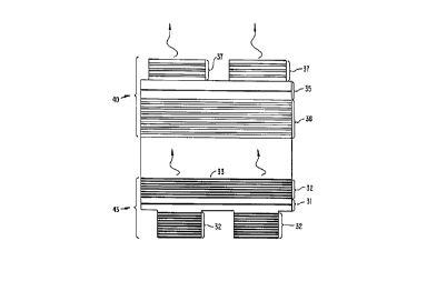
Fig 3. is a schematic representation of a
generic conf iguration of the present invention . This
figure as well as sll~-c~ n~ device Figs. 4-7, 9-11, and
17-18 show two short wavelength VCSELs 43 optically
pumping two long wavelength VCSELs 40. This configuration
is not intended to be limiting, but to indicate
schematically the wafer-scale nature of the fabrication
technology. This same technology can be used to make
WO96132766 P~ llu,, 'IA7~7~
21 90843
single devices consisting of one short wavelength VCSEL
pumping one long wavelength VCSEL, or to make large one
and two ~ nA l arrays .
Lasers 43 are a pair of electrically pumped,
short wavelength VCSELs. They are comprised of a short
wavelength active region 31 interposed between short
wavelength mirrors 32. Short wavelength radiation is
emitted from a top surface 33 of VCSELs 43 into the
bottom surface of a second pair of VCSELs 40. VCSELs 40
are a pair of long wavelength VCSELs comprised of a long
wavelength active region 35 interposed between a bottom
mirror 36 and top mirrors 37. Mirrors 36 and 37 are long
wavelength mirrors . Mirror 3 6 is transparent to the short
wavelength radiation emitted by VCSELs 43. Long wave-
length radiation is emitted from top mirrors 37. Modula-
tion of the long wavelength radiation is accomplished by
modulating the short wavelength pump VCSELs. In an
alternate: -'i l., modulation is accomplished by
applying contacts to the long wavelength VCSELs.
Fig. 3 and s~l~co~7d; n~ device schematics show the
short wavelength VCSEL bottom mirrors 32 and long wave-
length VCSEL top mirrors 37 as vertically etched to form
cylindrical posts. ~hese posts divide up the initially
planar wafer into many refractive index guided devices.
Index guiding is well known in the art, and can be
accomplished by etching, lateral oxidation, implantation,
11
Wo96/32766 21 90843 ~ r~
diffusion, ~ L~ ~1, or selectiv~ growth. In the
pref erred ~ ' ; r ~, both short wavelength and long
wavelength VCSELs should be index guided, although the
short wavelength VCSELs could be gain guided or t h~rr- 11 y
lensed.
The optically pumped configuration of Fig. 3
retains the advantages of VCSELs in general, such as the
possibility of wafer-scale fabrication and testing, and
inPyp~nhive one and two dimensional array fabrication.
This is in marked contrast to VCSELs which used solid-
state, dye, or in-plane sPmi c~nA~lctor lasers as the
optical pump. Optically pumped VCSELs which employ these
latter approaches are impractical for array applications
and cannot be manuf actured or tested on a waf er scale .
Fig. 4 is a schematic representation of one
of the invention. Long wavelength VCSELs 40
employ a wafer-fused, undoped, GaAs~AlAS mirror 41 on the
bottom side, and Al-~lect~ic mirrors 42 on the top side.
Dielectric mirrors 42 are formed from alternating layers
of silicon dioxide, SiO2, and titanium dioxide, TiO2.
Dielectric mirrors 42 can also be formed using other
dielectric materials. Long wavelength VCSELs 40 are fixed
to short wavelength VCSELs 43 by means of transparent
optical adhesive 44 between GaAs substrates 45 and 46.
Fig. 5 is essentially the same ~mhoA jr~ ~ as shown in Fig.
4 except GaAs substrate 45 of long wavelength VCSELs 40 is
12
WO 96132766
21 90~43
wafer-fused to GaAs substrate 46 of short wavelength
VCSELs 43 at an interface 50. This approach eliminates
the need for an optical adhesive, possibly leading to a
reduction in parasitic reflections. In an alternative
~ shown in Fig. 6, GaAs/AlAs mirror 41 can be
grown in the same epitaxial step as VCSELs 43, thus
eliminating the need for either an optical adhesive 44 or
wafer fusion 50 at this interface.
Fig. 7 is a schematic representation of an
alternate ~ L of the invention. Long wavelength
VCSELs 40 are comprised of a long wavelength active region
60 interposed between two GaAs/AlAs mirrors 61. Active
region 60 is wafer-fused to mirrors 61 at interfaces 62.
In the: ~-'i- L shown, the double-fused structure is
joined to short wavelength VCSELs 43 with optical adhesive
44. The double-fused structure can also be wafer fused to
VCSELs 43 as illustrated in Fig. 5.
Flg. 8 is a schematic Le~res,:l,Lation of an
~mhoni~-nt utilizing integrated microlenses. As in the
previous ~ ts, multiple short wavelength VCSELs 43
are used to optically pump multiple long wavelength VCSELs
40. However, in this: _'i--rL the arrays of VCSELs are
separated by a ~e ~nic~l spacer 70. Between the arrays
of VCSELs are a set of GaAs microlenses 71 which are used
to focus the radiation from VCSELs 43 into VCSELs 40.
Microlenses 71 are formed directly in the GaAs substrate
13
WO 96l32766 2 1 ~ 0 8 4 3 r~ n7~
72 of the short wavelength VCSELs (5hown), directly in the
GaAs substrate of the long wavelength VCSELs (not shown),
or both. Thus a large diameter, short wavelength VCSEL
can be used to optically pump a smaller .ll; t~r, long
wavelength VCSEL. This conf iguration allows higher power
outputs to be achieved in the long wavelength VCSEL. In
an alternate c '~ , microlenses 71 are formed of a
material other than GaA6, such as glass or a ref lowable
polymer. In this alternate configuration microlenses 71
are not mono-lithically integrated with the other parts of
the device.
Fig. 9 illustrates an alternate technigue of
att~rhin~ long wavelength VCSELs 40 to short wavelength
VCSELs 43. In this approach the two pairs of VCSELs are
joined at a metal interface 75 using metal to metal
bonding. A set of windows 76 in metal interface 75 allow
the pump radiation to pass through. Microlenses can be
in~uL~uL~ted into the windows (not shown). Although a
variety of metals can be used for the bonding metal, the
preferred ~mho~l;r L uses either pAllA~ or indium
containing solder.
Fig. 10 is a schematic representation of an
, ~ ~('ir -t.. of the invention in which VCSELs 40 utilize
dielectric mirrors 80 and 81. By using optical adhesive
44 to join VCSELs 40 to VCSELs 43, this ~hoAi--- t does
not require the use of the wafer fusion process. In an
14
~ W0 96/32766 2 ~ 9 0 8 4 3 ~ ,J,,,6/tl7~?~
alternate Dmho~ l" dielectric mirror 81 is joined to
VCSELs 43 using a dielectric to Spmi con~ tor bond which
is known in the art.
In the p~hor~ of the invention shown
schematically in Fig. 11, long wavelength active region 60
is interposed between dielectric mirror 42 and a bottom
mirror 90. Nirror 90 is formed by epitaxially growing
alternating layers of InP and InAlAs . To create the f inal
mirror the structure is etched, ~e~osin~ the aidFl 11 a of
the InAlAs material. The A1~lmin~m in the InAlAs is then
oxidized in from the sides, creating Tn~Al~A~rO, which has
a much lower refractive index than InAlAs or InP. The
result is that a low ref lectivity mirror is converted to a
high ref lectivity mirror . The lateral oxidation technique
can also be accomplished with ~ containing
mi n--m and antimony.
Fig. 12 shows the reflectivity graphs for two
particular mirror designs for an Dmhorl;- L of the
invention in which short wavelength VCSELs 43 emit at 980
nanometers and long wavelength VCSELs 40 emit at 1550
nanometers. Graph 100 is the reflection spectra for a
GaAs/AlAs mirror 6uitable ~or the bottom mirror of VCSELs
40. This mirror transmits the pump wavelength and
reflects the long wavelength of VCSELs 40. Graph 101 is
the rpelect;on spectra for a Sio~/Tio2 dielectric mirror
suitable for the top mirrors of VCSELs 40. The dielectric
WO 96/32766 2 1 ~ 0 8 4 3 PcrluS96/02323
mirror can be designed to either transmit or reflect at
VCSEL 43's wavelength. If the dielectric transmits at
this wavelength, as shown in plot 101, then VCSELs 40 only
see one pass of the radiation from pump VCSELs 43. If the
~ielec~- ic reflects at the pump wavelength (not shown),
then VCSELs 40 see two passe6 of the radiation from pump
VCSEls 43. By making the dielectric mirror partially
reflecting it iB poBBible to design a double-pass
configuration which increases the absorption and therefore
the pumping efficiency. It is also possihle to make both
the top and bottom mirrors of the long wavelength VCSELs
partially reflecting at the pump wavelength, creating
resonant pump absorption and an increase in pumping
efficiency. This last configuration, however, is
lS difficult to implement.
Fig . 13 is a schematic L ~yresentation of a
~pecific long wavelength VCSEL suitable for use in this
invention. Two lattice matched InGaAs quantum wells 110
are placed on two peaks of the optical standing wave.
Quaternary InGaAsP material 111 ~uLLuu-.ding these wells
absorbs the pump radiation and funnels the charge carriers
into the wells where they re-emit at 1550 n~r ~t~ s. The
absorption coefficient of this material is on the order of
1.5 X lO~ cm~l, so for the lengths indicated 90 percent of
the incident radiation is absorbed in two passes through
the cavity. Fig. 13 also shows that the long wavelength
16
WO 96/32766 2 ~ 9 0 8 4 3 ~ J~ 7~7~
cavity has a larger tLC~I~s~ ne dimension 112 than the pump
L ~I.nv~arae dimension 113. This ensures not only more
efficient conversion Or the pump radiation into the long
wavelength radiation but also single transverse mode
operation by the long wavelength VCSEL. In the preferred
L, transverse dimension 112 Or the long wave-
length VCSEL is defined by a lateral refractive index
variation (i.e., index guided). The index variation can
be defined in any or all of the vertical layers of the
device, and can be accomplished by t~h~mic:ll etching,
regrowth, implantation, diffusion, disordering, selective
growth, or other techniques. Index guiding is well known
in the art of semiconductor lasers.
Fig. 14 is a detailed energy band diagram of the
prererred absorber design ~or the ~'ir ~ shown in Fig.
13. The vertical axis of this diagram represents vertical
distance in the ~LLU~:LULe while the horizontal axis
represents relative energy. Graph 114 shows the energy
level as a ~unction of vertical distance for the valence
band. Graph 115 shows the energy level as a function of
vertical distance for the conduction band. In this
~-mhorl i r t absorbing material 111 is compositionally
graded to create a built-in electric f ield. The built-in
electric field aids in the speed and erficiency with which
photoyel~c L~ted charge carriers are collected in quantum
wells 110. In this design absorber 111 is comprised o~
17
W096132766 2 1 q0843 r~ Jv L~
compositionally graded InGaAsP 116 and 117. Portions 116
are graded from 1.15 micrometer bandgap material on the
bottom to 1. 3 micrometer bandgap material on the top .
Portion6 117 are graded from 1. 3 micrometer bandgap
material on the bottom to 1.15 micrometer bandgap material
on the top. A buffer layer 118 of InP i8 al~o shown in
this diagram. Although Fig. 13 and the following calcula-
tions assume lattice matched quantum wells, ideally
quantum wells 110 should be , ~s6ively strained with
re~ipect to the nu~ ~ ~,u.-ding layers.
The power at 1550 nanometers ver~us the power at
980 nanometers, the wavelength of the pump VCSEL in the
preferred P"~ho~;- L, is given by:
(1) P!5= (P9~ -- P~ 1calv ~T/ (T+A) ]
where
fraction of injected photon~
recombining radiatively in the wells
'1C~v = energy 105s from 980 nm to 1550 nm
~ 980/1550 = 0. 63
T = fractional transmission of output
mirror at 1550 nm
A = fraction of light lost to
absorption/scattering/diffraction per roundtrip
P,h = pump power required to reach
2 5 thresho ld .
18
W096~32766 2~ q08~3 P~ 6~
The thre6hold pump power can be calculated using the
quantum-well gain curve shown in Fig. 15. To reach
threshold, the quantum wells must provide a luulldLLip gain
equal to the luu--lLLip loss, which is T + A. Since the
cavity is free of dopants, the L~Ju~ldLrip absorption/scat-
tering/diffraction losses can be very small, approximately
0.1 percent. Given an output transmission of 0. 3 percent,
the threshold gain is 0 . 4 percent.
If both wells are pumped equally, a rP~n~hl e
assumption for double-pass absorption, each well must
provide a l~ul-.lLLip gain of 0.2 percent, or 0.1 percent
per pass. Given a well width o~ 80 a~ ,LL, -, this
requirement can be converted to a gain per unit length of
1250 cm~. This value can be converted into the required
current or power density using Fig. 15. Since Fig. 15
does not include the periodic gain Pnh;~n- L of 2 when
the quantum wells are at the stand-ing wave peak, the
appropriate value for the gain per unit length is 1250/2 =
625 cm-l. According to Fig. 15, achieving 625 cm~~ gain
requires 270 A/cm2. The total required current density is
540 A/cm2 since there are two quantum wells or,
equivalently, the absorbed power density must be 680
W/cm2. A~Ss~7min~ 85 percent of the pump radiation is
absorbed, 800 W/cm2 is needed to reach threshold. If this
power is uniformly distributed over a 10 micrometer
diameter VCSEL, then the total required power is 0 . 6 mW to
19
Wo 96~2766 ~ IA7'~
~l qOP~43
reach threshold. Since some of the injected carriers may
di~fuse laterally outside the optical mode, the number of
injected carriers required to reach threshold is higher
than this number. Therefore, to te for the lost
carriers, the threshold power is adjusted to 1. 0 Mw.
Fig . 16 shows a graph of equation 1 A~ m j n~
- 0.85 and 'Ala~v = 0.63. Fig. 16 illustrates that for this
specif ic amhorl; ~ ~~ 1, of the invention, approximately 1 mW
of output power can be achieved with a 980 nanometers pump
power of 4 mW. By increasing the pump power, improving
the absorption efficiency, or using a more advanced gain
medium, the output power can be increased. Higher output
powers can also be obtained using the configuration
illustrated in Fig. 8.
The po~r.~ ut versus power-in graph of Fig. 16
is shown as linear over a large power range. Typical
electrically pumped VCSEL curves show a rollover at large
drive currents due to heating. This effect is not shown
in Fig. 16 since heating during optical pumping is far
less than during electrical pumping. For example, the
thermal i ~ n~-e of the ~LLUL.LULe shown in Fig. 4 is on
the order of 1 K per mW. This means that 1 mW of heat
dumped into the cavity will result in a temperature rise
of 1K. In the example discussed above, a 4 mW pump was
re~uired to generate 1 mW of long wavelength output. Even
if all of the r~ ;nin~ 3 mW's is converted to heat, an
WO96l32766 21 908~3 PCrfUSg6/02323
unlikely oc. ~ ce, the result would only be a temper-
ature rise of 3 R in the long wavelength cavity . In
marked contrast, in an electrically pumped VCSEL several
tens of degrees K temperature rise could be expected.
In another: ';~~ t of the invention, the long
wavelength radiation p-~,~ay~tes in a direction opposite
that of the pump radiation. Fig. 17 is a schematic
representation of one possible conf iguration of this
~ _ ~ i L . In this conf iguration short wavelength active
region 31 is interposed between short wavelength mirrors
85 and 86. Mirrors 86 reflect essentially 100 percent of
the short wavelength emission, but are essentially
tran:,~aLel,t to the long wavelength ~miq~ n. In an
alternate configuration schematically illustrated in Pig.
18, long wavelength VCSELs 40 are slightly angled in
relation to short wavelength VCSELs 43. The angling of
the two arrays allow the long wavelength radiation to
bypass short wavelength mirrors 86.
As will be understood by those familiar with the
art, the present invention may be ~mho~l;Pd in other
specific forms without departing from the spirit or
essential characteristics thereof. Accordingly, dis-
closure of the preferred ~mho~; - t of the invention is
intended to be illustrative, but not limiting, of the
scope of the invention which is set forth in the following
claims .
21