Note: Descriptions are shown in the official language in which they were submitted.
2 1 90938
.
COMPUTER GRAPHICS CIRCUIT
FIELD OF THE INVENTION
Field of the invention
The described invention provides a computer graphics circuit to ren-
der image of light-reflected shading. The circuit is concerned in particu-
lar with Phong-.~h~ing with diffuse and specular reflection, and bump-
mapping to express a wrinkled or dimpled surface without geometric
shape modeling. The bump normal is defined with two-dimensional pat-
tern and stored in memory device. It is mapped onto the surface of ar-
bitrary direction. This technology is applied to the rendering processor
of a virtual reality and multimedia system(e.g.~ amusement, simulation~
to ~nim~.te realistic images in real-time.
Background Art
1. Background art of Phong shading circuit
Phong-.sh~ling is a typical light-reflection model in computer graph-
ics. To design the Phong-shading circuit in hardware needs following
processing; defining surface and light-source normals, calculating diffuse
and specular reflections, and combining these two reflective intensities.
In conventional approach, there was a circuit to define the normal of
surface with angular parameter of horizontal and vertical angles relative
to eye-point axis. The circuit based on this definition was simple due
to a necessity of only one set of memory device for each angle. In the
Phong sh~ling model, reflection intensity Ip is defined by addition of
2 1 90938
diffuse and specular reflection intensities. In conventional methods, a
horizontal reflection component Iph and a vertical reflection component
Ipv were calculated independently and added these two at final process-
ing. To combine the horizontal and vertical intensities as a mean value,
however, has a serious calculation-error at specified angles(e.g., O and
90 degrees). T_is invention is done to provide a Phong .~h~rling circuit
in order to minimi7e above error.
2. Background art of Bump mapping circuit
Bump-mapped .~hA~ling is obtained by following processing; d~fining
bump-normal, mapping the bump-normal onto surface, and calculating
diffuse and specular reflection intensities with intensity of light-source
and reflection angle against the surface. To map a colored pattern-
texture onto surface using hardware circuit has been known, however,
there is no practical circuit now for bump mapping. In practice it has
been primarily implemented in software or parallel processing architec-
ture using multiple arithmetic elements. Thus, it is very dif~cult to get
a rendering speed around million polygons per second in conventional
schemes.
This invention is carried out to establish the hardware circuit of
bump-mapped shading with a rendering speed within a single clock, in-
cluding the calculation combined with bump-mapping and Phong shad-
ing. The single clock of rendering speed means that a calculation result
can be obtained asynchronously and it takes only delay-times for switch-
ing speed of circuit.
This invention is useful for virtual reality system which needs an
- 21 90938
animated image in real time.
SUMMARY OF THE INVENTION
This invention of claim 1 specifies a bump-mapped sh~ling circuit
comprising: (1) span processors to fill the polygon by interpolating at-
tributes and coordinates defined at each polygon vertex, (2) a reverse-
projection circuit(texture mapping circuit) and bump-pattern RAM (random
access memory), which stores a function table of bump normals in a
two-dimensional array, (3) a bump-mapping circuit which rotates the
surface angle with the bump-mapping angle, and (4) a shading circuit
to compute the diffuse and specular intensity of the bump-mapped sur-
face reflecting multiple light-sources.
In the above-described system, the normal vectors of the polygon-
surface, light-sources, and bumps are defined by two values, horizontal
and vertical angles. Surface normals and light-sources are defined with
angles relative to the eye-point axis in device coordinates, and bumps
are defined relative to the axis perpendicular to the texture mapping
address. The Phong sh~ling model is formulated with the trigonometric
functions which include either horizontal or vertical angles.
Surface angle and texture coordinates are given for each polygon ver-
tex and interpolated along the outline of the polygon first. Then span
processors interpolate these attributes and coordinates inside each poly-
gon. The bump-angle stored in RAM iS read by the address given by the
reverse-projection circuit. The bump-mapping circuit receives both the
surface angle from the span processor and the bump-angle from the RAM
and rotates the surface angle with bump-angle.
2 1 90938
The rotated surface angle determined by the bump-mapping circuit
is given to the shading circuit, implemented with diffuse and specular
reflection circuits, which compute the reflected intensity on the surface
min~ted by the light-sources. This computation is carried out for
every point on the polygon-surface, synchronized with the execution of
the span processor. The surface ~h~ling is obtained by multiplying the
reflected intensity with the texture pattern color.
The invention of claim 2 defines the array of the bump-pattern in the
same 2D coordinates as the texture pattern. This pattern-coordinate
is defined at each polygon vertex not only for the texture but also
bump-mapping, and applied simultaneously to both texture pattern and
bump-angle RAMS, after the address is projected reversely to the tex-
ture pattern coordinate from the device coordinate which a perspective
projection may be applied.
The invention of claim 3 uses the memory-table for bump-normal
rotation to define trigonometric functions of either horizontal or vertical
surface angle input-variables for rotation of bump normal with surface
normal in the bump mapping circuit.
The invention of claim 4 handles the lighting in the shading circuit
with the memory tables, multipliers and adders. The memory tables
which receive either horizontal or vertical input-variables rotated the
surface-normal with the bump-normal at the bump mapping circuit are
used to define trigonometric functions.
The invention of claim 5 is to get the textured and bump-mapped
shading surface by multiplying texture colors with red, green and red
with shaded intensity at the bump-mapped sh~ling circuit.
2 1 9093~
The invention of claim 6 comprises the RAMS for specular exponent
table and trigonometric function tables which includes the light-source
components while the ROM for trigonometric function table which in-
cludes only normal component of surface or bump.
As per the above description, this invention provides real-time render-
ing of light-reflected three ~lim~n~ional images in a hardware implemen-
tation with a small-scale circuit and with small errors. To implement
the bump-mapping processing in hardware brings several thousands of
higher speed than the processing by software.
BRIEF DESCRIPTION OF THE DRAWINGS
Fig. 1 is a block diagram of the Phong-shading circuit in a parallel
light-source system;
Fig. 2 is a block diagram of the bump-mapped shading circuit illus-
trating data-flow and total organization;
Fig. 3 is a block diagram of another example of the bump-mapping
circuit;
Fig. 4 is a block diagram of the bump-mapped shading system using
rotation matrix and vector forms for the rotation of surface and bump
normals;
Fig. 5 is a block diagram of the detailed circuit of Fig. 4;
DETAILED DESCRIPTION OF THE PREFERRED
IMPLEMENTATIONS
~1. Shading circuit
2 1 90938
This invention defines the normal vector of surface and light-sources
as horizontal and vertical angles relative to eye-point axis in device co-
ordinates. Equations in a conventional expression using normal vectors
can be rewritten as trigonometric functions of only one variable, ei-
ther the horizontal or vertical angle of surface and light-source. To use
these angle-values, the cosines can be expressed as: cos~ = cosNv x
{cos LV[cos(Lh--Nh)--1]} + cos(Lv--Nv~ (1)
cos ~ = 2 cos Nh x cos NV x cos ~--cos Lh cos LV
cos ~ ~ (cos ~ + cos Nh cos NV)/2 (2)
where Nh and NV are the horizontal and vertical angles of the surface
normal, respectively, and Lh and Lv are the horizontal and vertical an-
gles of light-source normal, respectively. Equations (1), (2), and (3)
do not contain combinations of multiple angle-components in division
or multiplication forms such as Nh/NV or NhXNv in the trigonometric
functions.
The mathematical model of Phong-shading is expressed with follow-
ing equation:
I = Ia + Ip = Ia + Id cos(~) + Ir cosn(o~) (3)where Ia is ambient light, Ip is reflected light, Id and Ir are diffuse and
specular reflection coefficients respectively, n is the specular exponent,
~ is the angle between the light-source and surface normal,and ~ is the
angle between a mirror-reflected direction relative to the surface nor-
mal and the viewing direction. Overall intensity can be obtained by
adding environmental or ambient light Ia to reflected light Ip. Intensity
Ip is computed at all points of a polygon surface using the interpola-
tion scheme for coordinates, normal vectors and other attributes being
21 9093~
defined at the polygon vertices.
The variable-range of Nh and Nv is chosen to be about 10 bits. Thus,
each trigonometric function has 1024 words RAM or ROM. (If two angle-
variables were combined, the variable-range becomes 20 bits and 1 Mbit
RAM iS needed, difficult to implement in an ASIC.) The concatenated
values of multiplied trigonometric functions, such as cos Nh cos Nu cos ~,
are rounded-off to the specified significant bit-length corresponding to
the necessary accuracy of image quality. The trigonometric functions in
equations (1) and (2) contain the light-source angles Lh or Lv with Nh or
Nv~ However, the light-source normal can be regarded as a unique and
constant-value every video-frame cycle in the parallel lighting. Thus,
all trigonometric functions in equations contain a single variable. The
circuit based on equations can be implemented with memory devices,
multipliers and adders. The cos" c~ is defined by a RAM table.
Attention is directed to Fig. 1 which shows the Phong-shading circuit
of the invention based on equations (1), (2), and (3). Input variables
in the circuit are the horizontal angle Nh and vertical angle NU of the
surface normal. This circuit computes cos~ and COSQ' using memory
devices 1 - 4, multipliers 5a and 5b, and adders 6a and 6b. Memory
devices 1 and 3 are RAMS. RAM1 and RAM3 store the terms of equation
(1), cos Lv[cos(Lh--Nh)--1] and cos(Lu--Nv), respectively. Memory
devices 2 and 4 consist of ROM and store cosNu and cosNh, respectively.
The adders 6a and 6b output cos~ and 2cosc~, respectively. The
diffuse reflection term is obtained by multiplying cos~ with the diffuse
coefficient Id. The specular reflection term can be obtained by multiply-
ing the specular coefficient Ir with the COSQ' output from RAM7. RAM7
21 90938
~ ,
stores the cosine-exponent table of cosn. The output values of cos ~ and
cosn Cl have double bit-length at the multiplier of 5a or 5b, rounded to the
specified significant bit-length. In the case that high accuracy is needed
under high-specular exponent value, a linear interpolation approxima-
tion scheme can be employed using RAMS and multiplier instead of RAM7.
As described by equation (1), intensity with the Phong-shading model
is obtained by the addition of Id cos ~ and Ir cos" ~.
2. Bump-mapping circuit
Bump-mapping rotates the surface normal (angle) with a bump nor-
mal. Interpolation for polygon filling is applied to the coordinates, tex-
ture mapping address, surface angle, and light-source angles (in a mul-
tiple light-source system). The bump-pattern is allocated in two dimen-
sional u, v coordinates with a functional variable defined by horizontal
and vertical angles, Bh and Bv, relative to the the axis perpendicular
to u,v coordinates. This pattern is stored in the RAM. The bump-
mapped surface may be scaled and applied a perspective projection,
which needs to invert the u, v device-coordinates to texture coordinates.
After this reverse-projection computation, the address is applied to the
bump-pattern RAM. This address is the same as that applied to the tex-
ture pattern RAM. However, maintaining the same significant bit-length
as the texture pattern address is not necessary, due to differences in
resolution.
The bump-mapping circuit rotates the N" and NV angles with Bh and
Bv to obtain angles Nh and Nv. This invention represents the rotation
function with a trigonometric function of one variable, either Bh or Bv.
;~1 90938
This equation is given by following equations: NV = arcsin(cos Nu sin BU+
sin Nv cos Bh cos Bv)
N,~ = arcsin sin Bh cos Bv/~ sin2 NU + Nh (4)
where
~B = arccostsin I Bh I cos Bu) sin Bh
m = arcsin(sin Bu/ sin 1 ~' 1) (5)
putting sin Bh as following:
Bh >
O Bh=O
Bh <
then equation (4) is transformed by following equations:
Nh = arcsin(cos ~ /1--sin2 Nv)s( _ l)U + (--l)Su7r + Nh
u: O I Nu + m 1< 1r/2
I Nu + m 1> 1r
s: O ~ < O
-,~ > O
putting t = sin(Nu + m) sin I ,(3 1,
Nh = Nh + arcsin(cos ¦ ,l3 ¦ /~)s(--1) + (--1) u~r
Nv = arcsin(sin(Nv + m) sin I ~ 1) (6)
Equations (5) is a function defined by the horizontal Bh and vertical
BV angles of the bump normal and these two modified angle-variables,
~B and m, are stored in the bump pattern RAM instead of Bh and Bv to
reduce circuit complexity. In equation (6), Nh and Nv are represented by
trigonometric functions such as sin(Nu+m), sin,(~, cos,B, and t, where the
significant bit-lengths of variables in the trigonometric functions take the
21 90938
range of one angle or an angle plus 1 bit, allowing circuit implementation
with trigonometric function-tables using small-capacity memory devices.
As shown in equation (6), all of the trigonometric function table in the
bump-mapping circuit can be implemented with ROMS.
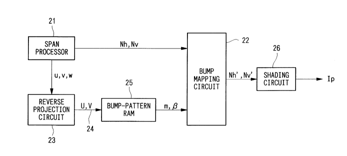
Attention is directed to Fig. 2 which shows the block diagram of a
bump-mapped .sh~ling circuit. Circuit 21 iS a span processor which
interpolates the surface angle Nh and Nv~ and texture coordinates u, v.
The N" and Nh parameters are passed to bump-mapping circuit 22, while
ll,V coordinates are given to the reverse-projection circuit 23, which
transforms the u, v address to texture coordinates. The reverse-mapped
address 24 is then applied to the bump-pattern RAM25. In the pattern
RAM"B and m are stored instead of the Bh and Bv to avoid computation
of equation (5). The output data of RAM 25 is transfered to the bump-
mapping circuit synchronizing with the generation of DDA of Nh and Nv
in span processor 21.
In a perspective projection system, the reverse-projection transfor-
mation is applied to Nh and NV because these angles are defined in
device coordinates. If the normal vector is not applied to perspective
transformation in mapping the world coordinate system to the device
coordinate system, application of the reverse-projection transformation
for Nh and Nv is not needed.
The modified bump-angle variables ~ and m are applied to the bump
mapping circuit in Fig. 2. At this time, the filtering for scaling may be
applied. In circuit 22, operations based on equation (6) are executed,
outputting Nh and Nv~ which are rotated the Nh and NV with the Bh
and Bv. Nh and N' are given to shading circuit 26, which is equivalent
~ 1 9093~
to the circuits of Figs. 1.
Attention is directed to Fig. 3 which shows the bump-mapping circuit
in the invention. The circuit is based on equation (6). The trigonometric
function-tables of 38, 39, 30, 31 and 32 consist of memory devices. These
memory devices could be based on RAM, but ROM iS used for all memory
tables. The surface angle N" and bump-angle m are added at adder 37a
and applied as (NU + m) to the sine RoM38. Bump-angle ~ is applied
to RoM39, which stores sin(~B) and cos(~) separately. At multiplier 33a,
t = sin(Nv+m) sin(,(3) is obtained, which is then applied to RoM30, which
stores the function 1/~. N' is obtained to apply the output data
of multiplier 33a to arcsin RoM31. Nh is obtained to multiply cos,B with
the output data of RoM30 at multiplier 33b and applied to the arcsin
RoM32 before adding to Nh at adder 37b. The upper bit of angle-value
is used for the sign of equation (6), so that the table is shared according
to the upper bit. As shown in Fig. 3, there is no feedback loop in the
bum~mapping circuit. It can output the result with only the delay of
memory devices, adder and multipliers. Thus, the bump-rotated angle
can be obtained within a clock cycle.
3. Bump-mapped shading circuit
Rotating the bump normal with the surface normal and rotating the
surface normal with the bump normal are equivalent. Thus, if the bump
normal represents a 3-axis component using the horizontal Bh and vçrti-
21 90938
cal Bv angles, a rotated angle is given by the rotation-matrix as follows:
X1 cos(Nh) O sin(Nh) 1 0 0 XO
Y1 -- o 1 0 0 cos(N") sin(N~) YO
Zl --sin(Nh) O cos(Nh) O --sin(Nv) cos(Nv) ZO
XO = sin Bh cos Bv; YO = sin Bv; ZO = cos Bh cos Bv (7)
The trigonometric functions in the above matrix parameters contain one
variable of either horizontal or vertical angle, so that the circuit can be
designed with small memory size. For shading computation, diffusion
angle cos ~ and specular angle cos c} in Phong-shading are given by fol-
lowing equations:
cos ~ = X1 cos Lh/ sin Lh + Y1 sin Lv
COS C~ ~ (COS ~+Z1)/2 (8)
Using equations (7) and (8), the circuit is implemented with memory
devices, multipliers and adders, which output bump-mapped shading
pixels at every clock cycle.
Fig. 4 shows the circuit of the invention. In Fig. 4, span processor
41 outputs the angle values Nh and Nv of surface and the u, v texture
address. The u, v address is applied to the reverse-projection circuit 42
where outputs the address to the RAM45. RAM45 stores the values of the
bump-angle function, XO, YO and ZO in equation (7). Nh and Nt, are
applied to the trigonometric function-tables 43 and 44, respectively. The
outputs of tables 43 and 44 are given to the rotation-matrix multiplier
46 as parameters in the matrix of equation (7), obtaining the cosines of
diffuse and specular reflection. These cosines are multiplied with texture
pattern color in circuit 47.
Attention is directed to Fig. 5, which shows the circuit in this inven-
12
2 1 9093~
tion based on Fig. 4. In Fig. 5, surface angles Nh and NV are applied to
trigonometric function tables 51 - 54, where RoM51, RoM52, RAM53 and
RAM54 store cos NV, sin Nv, sin Lh cos L" cos Nh, and sin Lh cos Lv sin Nh,
respectively. These output data are applied to multipliers 55a - 55h
and multiplied with X0, Y0 and Z0, based on equation (7). The output
data of multipliers 55a - 55h are then applied to adders 56a - 56d, re-
spectively, to obtain Xl, Yl and Zl in matrix equation (7). Xl and Yl
are multiplied by cos(Lh)/ sin(Lh) and sin(L~,) at multipliers 55j and 55i,
respectively, and then cos~ and coso~ are obtained via adders 56e and
56f, respectively. The 1/2 coefficient in Fig. 5 shows the 1 bit shift-down
circuit. In Fig. 5, it is obvious that RAMs 53 and 54 can be replaced
with ROMS if the sinLh and cosLv are replaced with ROM tables and
multipliers.
As per the above-described implementation, this invention has the
features that (1) the normals for surface and light-source are represented
with two angle values, horizontal and vertical angles relative to the eye
point axis in device coordinates, and use trigonometric function tables
with ~imil~r ranges of single angle variable (equations (1) and (2)), (2)
the bump-pattern normals are defined by horizontal and vertical angles
relative to the perpendicular to the u,v-axes and addressed with the
same address as the texture pattern, storing its pattern as a modified
bump normal value (equations (5) or (7)), (3) the bump-mapping circuit
rotates the bump normal with the surface normal or rotates the surface
normal with the bump normal before applying the shading circuit using
the trigonometric function ROM tables.
This invention is applied for the arithmetic operation circuit of graph-
13
2 1 90~3~
ics processor to be used for amusement and computer simulation due tothe use of small scaled ASIC. This technology provides an important
visual technology of computer graphics to establish the virtual reality
system.
14