Note: Descriptions are shown in the official language in which they were submitted.
WO 95/32568 ~ 19 0 9'~ 0 pCT/GB95/01175
1
OPTICAL PACKET PROCESSING
BACKGROUND TO THE INVENTION
The present invention relates to a method and
apparatus for processing a multi-bit packet carried on an
optical network. Typically the package might comprise an
ultrafast binary data signal having a bit rate of 10 Gbit/s
or more and carrying e.g., telecommunications traffic.
The term packet as used herein encompasses both
asynchronous packets as transmitted, for example, in an ATM
system, and packets of synchronous data, such as frames in
a synchronous OTDM system.
Ultrafast binary data signals can be generated quite
readily in return-to-zero (RZ) format by using a source of
ultrashort e.g. (picosecond) pulses at a repetition
frequency which is a sub-multiple of the required bit rate.
These pulses are then each split into a number of separate
optical paths, modulated using electro-optic devices, time-
delayed and then recombined so as to interleave them to
achieve an ultrafast bit rate [ 1 ] . Since this bit rate may
be beyond the speed capability of electronics, any
subsequent signal processing (such as retiming,
regeneration or demultiplexing) must use all-optical
technologies. This in turn in general will require the
provision of an optical clock signal in precise
(picosecond) bit synchronisation with the data.
Whilst in ultrafast circuit-switched or synchronous
transmission systems, clock recovery can be carried out
using phase-locked loops, this is not possible for
asynchronous transmission systems and especially
asynchronous packet-switched systems because clock recovery
has to be performed on a packet-by-packet basis in a small
fraction of the packet duration. This would require a
219t~9'~0
W0 95/32568 , PCTIGB95/01175 I
2
phased-locked loop with an extremely short acquisition time
(possibly as short as a few tens or hundreds of
picoseconds). Even if the loop round-trip delay in an
optical phase-lock loop could be reduced by making the
optical path lengths very short by using e.g. some kind of
integrated optical device, for the phase-lock loop to work
robustly it would still require a large number of signal
pulses to acquire lock with sufficient phase-error signal
quality and with sufficient lock-in range. The acquisition
times would therefore still be much longer than the packet
duration in a packet-switch system. Moreover even if
locking could be achieved in time, the short acquisition
time would then make the phase-locked loop more sensitive
to disturbance by noise.
In view of these problems, it has previously been
proposed [ 7 J to transmit a comb of clock pulses before each
data packet. Then at each position in the network where
signal processing of the packet is to be performed, the
comb of clock pulses is separated from the data using
optical couplers, fast photodetectors, electronic sense
circuitry and an optoelectronic space switch. However this
approach has serious disadvantages. Firstly, the payload
traffic capacity of the network is reduced by the
additional overhead associated with the transmission of the
comb of clock pulses. Although this might be minimised by
transmitting only a relatively short segment of the clock
comb there would nonetheless have to be a time guard band
between the clock comb and data packet long enough to
accommodate the time uncertainty in the sense circuitry and
the commuting time of the optoelectronic switch. This
guard band may need to be as long as 0.5-1 ns, equivalent
to 50-100 bit periods at a data packet bit rate of 100
Gbit/s. A second disadvantage is that the clock comb, or
segments of it, will be subject to the same transmission
impairments as the data packet, suffering, for example,
amplitude noise and timing fitter arising from effects such
WO 95/32568 219 8 ~ ~~ ~ t' ' pCT/GB95/01175
3
as amplifier noise and fibre acousto-optic effects [8, 9].
This would limit the uses to which the clock pulse train
could be put.
Another proposal disclosed in Zhang et al.,
Electronics Letters, Vol. 29, no. 21, 14 October 1993, pp
1871-1873, uses clock pulses transmitted on a separate
wavelength channel from the OTDM packet. Since the clock
pulses are at a different wavelength, their phase
relationship to the frame varies as a result of dispersion
over the transmission path.
A paper published in Journal of Lightwave Technology,
vol. 11, no. 5/6, May 1993, pp 829-835 discloses a system
in which a synchronous stream of bits is divided up into
blocks and sub-blocks which incorporate timing bits in a
predetermined pattern. By means of several stages of logic
processing incorporating AND and OR gates a clock signal is
recovered from the predetermined bit pattern.
SUMMARY OF THE INVENTION
According to a first aspect of the present invention,
there is provided a method of processing a multi-bit packet
carried on an optical network,
characterised by transmitting with the packet a marker
pulse, and replicating the marker pulse and thereby
producing a clock signal at the bit-rate or a sub-multiple
thereof for use in a subsequent operation on the packet.
The present invention takes a single pulse from each
packet, the "marker pulse" and uses it to create a clock
pulse train by replicating the marker with the appropriate
pulse repetition frequency. Since no feedback loops are
involved, the technique can be used on a packet-by-packet
basis with minimal delay. By contrast with the prior art
WO 95/32568 219 0 9 7 0 pCT~GB95/01175
4
techniques, the network overhead is negligibly small
(typically around 1-3 additional bit periods per packet)
and the clock is recovered without needing complex logic
circuitry. Moreover, the clock pulse train is created with
great precision and substantially no amplitude or timing
fitter. The invention is particularly advantageous in the
context of asynchronous systems, where, as noted above,
there is a need for rapid acquisition of a clock for each
incoming frame. However it also offers advantages over
conventional clock recovery techniques for synchronous OTDM
frames .
Preferably, the recovered clock signal is used for
retiming the multi-bit packet.
As already noted, the clock signal produced using the
method of the present invention is substantially free of
fitter. It is therefore particularly suitable for use in
packet bit retiming.
The step of retiming may include introducing the
packet and the recovered clock pulse train into a non-
linear optical modulator, the cross-phase modulation of the
packet and the clock pulse train retiming the bits of the
packet when the packet is subsequently output onto a
dispersive medium.
This preferred form of packet bit retiming adapts the
soliton-shepherding technique disclosed in the present
applicant's co-pending international patent application
PCT/GB93/00863 (W093/22855).
Alternatively or in addition the subsequent bit-level
processing may include a stage of all-optical packet
regeneration. Preferably the recovered clock pulse train
is input to an optical switch and the switch is gated by
the incoming packet data stream, thereby producing at the
~ ~ WO 95132568 219 0 9 7 0 PCT/GB95/01175
~:
output of the switch a re-generated data stream. The
optical switch may be, for example, a non-linear loop
mirror (NOLM).
5 The method may include a stage of marker pulse
regeneration in which the marker pulse from the packet is
amplified or filtered or otherwise shaped prior to
replication.
Preferably the marker pulse has a fixed bit-
asynchronous time relationship to the other pulses of the
packet. The marker pulse can then be separated by ANDing
the packet header containing the marker pulse with a
delayed version of the header, the delay being such that
the marker pulse coincides at the AND gate with another
pulse of the header.
Other alternative means of distinguishing the marker
pulse from the rest of the data packet include the use of
a distinctive intensity, or polarisation for the marker.
Use of a distinguishing time relationship is generally
preferred since these alternatives all suffer the potential
disadvantage that the marker pulse may, as a result of
dispersion and like effects over a long optical path,
become separated from the other pulses of the packet. By
contrast if the marker pulse is distinguished simply by its
time position, then it will in general propagate in the
same manner as the other pulses of the packet. However, if
polarisation-mode dispersion is negligible, or if a soliton
marker is used, then distinguishing the marker by its
polarisation is acceptable.
According to a second aspect of the present invention,
there is provided an optical circuit for processing a
multi-bit packet carried on an optical network,
characterised by a marker pulse replication stage arranged
to generate from a marker pulse carried with the multi-bit
WO 95/32568 PCT/GB95101175
219Q9~Q
6
packet a clock at the packet bit-rate or a sub-multiple
thereof for use in a subsequent operation on the packet.
According to a third aspect of the present invention,
there is provided a method of processing a multi-bit packet
carried on an optical network characterised by transmitting
with the packet a marker pulse , subsequently generating an
optical word from the marker pulse carried with the packet,
processing the packet with the optical word, and outputting
the processed packet.
DESCRIPTION OF THE DRAWINGS
The present invention will now be described in further
detail, by way of example only, with reference to the
accompanying drawings in which:
Figure 1 is a schematic of a packet-bit retiming
circuit;
Figures 2a and 2b are an all-optical packet
regenerator and an optical switch for use in such a
regenerator respectively;
Figure 3 is a packet demultiplexer;
Figures 4a to 4d illustrate different methods of
distinguishing the marker pulse;
Figures 5a and 5b show methods of generating a clock
pulse;
Figures 6a to 6c show alternative circuits for
replicating the marker pulse;
Figure 7 is a schematic showing the layout of a
demultiplexer;
Figure 8 shows the layout of the delay line chip 1 of
Figure 7;
Figure 9 shows the layout of delay line chip 2 of
Figure 7;
Figure 10 shows a pulse regenerator for use in the
circuits of Figures 1 and 2;
Figure 11 shows an optical switch for use in the
circuit of Figure 2; and
WO 95/32568 219 0 9 7 0 PCT~GB95/01175
7
Figure 12 shows a circuit for regenerating selected
channels of a synchronous OTDM packet.
DESCRIPTION OF EXAMPLES
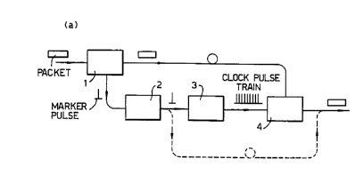
An all-optical packet regenerator includes a marker
pulse separator/duplicator (1; Figure 2) which receives at
its input an incoming OTDM packet. The
separator/duplicator 1 may replicate the packet using, for
example, a fibre 50:50 coupler. The original packet is
then output and passed on to a later switch stage. The
packet present at the other output of the coupler is
processed to recover and isolate a marker pulse carried in
the packet header. The marker pulse then passes to a
marker pulse regeneration stage 2 and onwards to a marker
pulse replicator 3. This replicates the marker pulse
using, for example, one of the techniques described in
further detail below, to produce a clock pulse train at the
packet bit rate. The clock pulse train is then input to an
optical switch 4 gated by the original packet.
Although, as discussed in the introduction, a number
of different methods are possible for distinguishing the
marker pulse from the packet, the preferred technique
adopted in the present examples uses a marker distinguished
by its time position in relation to the rest of the data
packet, and more particularly a marker which precedes the
rest of the packet by a fixed bit-asynchronous delay. For
example, the delay between the marker and the packet may be
1.5 T where T is the bit period of the packet. In this
case, the packet may include in its header immediately
following the marker pulse a bit which is always set to 1.
The marker pulse can then be derived from the packet by
applying the packet and a delayed version of the packet to
an optical AND gate, with the delay being set equal to the
distance in time between the marker and the f first following
WO 95/32568 PCT/GB95/01175
21909?0
8
bit of the packet, in the present example 1.5 T. This
procedure is shown schematically in Figure 5a.
Figure 5b shows a practical implementation. In this
implementation the AND gate is a semiconductor laser
amplifier. The original and delayed versions of the packet
input to the AND gate interact in the SLA by a process of
four wave mixing (FWM), as described in [16]. Independent
polarisation controllers such as BT&D MPC1000 are provided
in two input branches to the AND gate. The fixed delay is
provided by a length of polarisation preserving fibre 54.
The length of the fibre 54 is chosen so that group delay
difference for the two polarisation eigenmodes of the fibre
equals the required delay 1.5 T. For typical polarisation--
preserving fibre, such as high-birefringence fibre type
HB1500 manufactured by Fibercore Limited of Chandlers Ford,
Hampshire, England, specified as having a beat length of
less than 2 mm and with packets at a bit rate of 100Gbit/s,
the length required is less than 30m, giving a delay of
l5ps. The polarisation state of the incoming packet is
set to be linear, aligned at 45° to the fibre polarisation
axis. This splits the signal into two orthogonally
polarised components that emerge from the fibre with the
required l5ps time difference. These two orthogonally-
polarised time-shifted components provide the input signals
to the optical AND gate. As described in [16] the AND gate
requires pump light which is coupled into the polarisation-
preserving fibre through a second input branch with an
appropriate polarisation.
It is found that with such an AND gate, sharp
filtering is required on the output to separate the AND
signal from other features of the output. This however can
lead to an undesirable broadening in the output pulse
profile. To avoid this, the output is preferably filtered
using an ultra-steep edge high rejection fibre Bragg
grating filter. Such a grating may be fabricated, for
WO 95132568 PCT/GB95/01175
9
example, in hydrogen loaded (200 Bar) standard
telecommunications fibre (Phillips matched-clad) with a
nominal core-cladding index difference of 4.5 x 10 3. A 4mm
long grating may be replicated using an interfermoneter
based on a rectangular silica block and phase mask, as
described in Kashyap R, "Photosensitive optical fibres:
Devices and Applications", Opt. Fibre Technol., 1(1), 17-
34, 1994. One such filter can give extinctions greater
. than 64dB and edge widths less than lnm, and two such
filters cascaded with an interposed isolator can give
better than 74dB rejection.
Other methods of distinguishing the marker pulse from
the rest of the data packet include the use of a'
distinctive intensity, or polarisation as shown in Figures
4a, 4c respectively. Figure 4b illustrates the preferred
method, using time position.
Where the marker pulse is distinguished by its
polarisation state, (Figure 4c) for example if it has a
polarisation orthogonal to the rest of the packet, then
provided this orthogonality is preserved during
transmission the marker can be stripped off from the main
packet using a simple polarising beam splitter such as
SIFAM type PS15. Experimental evidence suggests that
polarisation orthogonality can be preserved over distances
as great as thousands of kilometres. For transmission of
the packet onwards from the node, a single orthogonally-
polarised marker pulse must be replaced at the head of the
packet. In Figure 2 discussed above, and Figure 1
discussed below, this is done using the dashed line optical
path to route a replica of the marker pulse to be combined
with the output packet with an appropriate time delay.
Once it has been recovered, the marker pulse is
treated by the pulse regeneration stage. This may operate
using e.g., amplification, spectral filtering, pulse
WO 95132568 ' PCT/GB95/01175
compression or soliton shaping to improve the quality of
the pulse. Figure 10 shows one example of a marker pulse
regenerator using nonlinear transmission characteristics of
an optical device to improve the pulse quality, as
5 described in "Pulse shaping, compression and pedestal
suppression employing a nonlinear-loop mirror" K Smith et
al., Optical Letters, vol 15 no. 22 pp 1294-1296 (1990). A
NOLM is used to suppress the amplitude noise and background
pedestal on a pulse and also to compress it in time. In
10 the circuit shown in Figure 10, the erbium fibre amplifier
could be model EFA2000 available from BT&D Technologies.
The bandpass filter could be the tunable device number
TB15090B manufactured by JDS Fitel. The fused fibre
coupler may be model no. SMC0202-9-2C50/212 and the
polarisation controller could be a manual controller'type
MPC1000, both available from BT&D. The fibre used for the
loop may be 200m of dispersion-shifted fibre, dispersion
zero at 1.6 microns wavelength, group velocity dispersion
-l.6ps/(nm-km) at 1.59 microns, as described in Smith et
al.
As a further alternative, the pulse regeneration stage
may include an optical source triggered by the incoming
marker pulse to provide a newly generated output pulse.
The marker pulse replicator may use one of a number of
different techniques for replicating the marker pulse to
create a precise clock pulse train. Figure 6a shows a
single-stage split, delay and recombine network which can
be fabricated using silica planar delay line technology
[19]. However, while this is suitable for shorter clock
pulse trains, if the pulse train is more than about 8
pulses long the single-stage network becomes unwieldy in
construction. Lt is then preferable to use a concatenation
of several binary split-delay-combine stages in shown in
Figure 6b. Using log2n stages a single input pulse is
converted to a train of n pulses with constant pulse
separation T. This arrangement has the advantage that the
. .._ wO 95/32568 219 0 9 7 ~ ; ,: .
PCT/GB95/01175
..
11
binary splitting and combining ratios can be chosen to be
different from 50:50 to compensate for transmission loss
asymmetry in each stage. Optical amplifiers such as
erbium-doped fibre amplifiers JDS Fitel type ErFA-1000 may
be inserted between stages as necessary to compensate for
both intrinsic and extrinsic losses.
An alternative approach illustrated in Figure 6c uses
an amplified recirculating loop device to duplicate the
input pulse. This comprises a short recirculating delay
line with optical gain. A fraction of the marker pulse
enters the loop through the coupler (C) and continues to
circulate around the loop with gain being provided by the
optical amplifier (A). The time delay associated with one
round-trip of the loop is equal to the bit period of the
packet or to an integer multiple thereof. A delay of 1
bit-period may be impractical at the highest bit rates.
For example, if we are working with a bit rate of 100
Gbit/s, the required round trip time would be just 10 ps,
implying a loop length of just 2 mm or less. It would be
more practical in the case that we want to replicate the
marker to create a pulse train at a sub-multiple of the bit
rate. For example, if we replicate every tenth pulse of a
100 GHz clock (pulse repetition period = 10 * 10 ps = 100
ps) the required loop length would be about 15-20 mm (i.e.
the loop diameter is approximately 6 mm). The actual loop
length depends on the refractive index of the materials
from which it is made. Supposing the loop consists of a
silica planar delay line (e.g. ref [19]) together with a
semiconductor optical amplifier device used as the
amplifier/switch, then we require (L1*n1 + L2*n2 + L3)/c =
T, where L1 is the path length of the silica planar delay
line with refractive index nl, L2 is the path length of the
semiconductor optical amplifier device with refractive
index n2, L3 is the total path length in air of the
interfaces between the silica planar delay lines and the
semiconductor device, c is the speed of light in vacuum,
WO 95/32568 219 d 9 7 0 PCT/GB95/01175
12
and T is the required optical round-trip time. Then if,
for example, T=100 ps, nl=1.5 (ref index of silica), n2=4
(typical semiconductor), L2=0.5 mm (typical semiconductor
device length) and L3=0.5 mm, we require L1=18.17 mm.
If we wanted to replicate the marker pulse so as to give a
train of pulses at the full bit rate and as long as the
packet (i.e. a train of perhaps several hundred pulses), it
might be useful to combine the recirculating loop (Fig 6c)
with an earlier passive replication stage (Fig 6a or 6b).
For example, if we use a passive replication stage to
create a train of e.g. 10 pulses at the full bit rate 100
Gbit/s, then the round-trip time of the recirculating loop
could be chosen to be 10 times the bit period (i.e. 100 ps,
as in the previous example) . There would then be 10 pulses
circulating continuously around the loop, providing a
continuous train of 100 Gbit/s pulses at the output
(continuous until the semiconductor amplifier/switch is
turned off). The semiconductor optical amplifier switch
could be, for example, BT&D type SOA 1100/3100.
In the ideal case, the coupler is a 3dB coupler, and
the amplifier gain is set to 3dB gain. This results in a
train of uniform intensity clock pulses which are half the
intensity of the incoming marker. The amplifier is
designed to be gateable electrically on a packet-by-packet
basis. This requires a response time of say lns or less,
and for this purpose a semiconductor amplifier would be an
appropriate device. This allows the replicator to be
rapidly quenched ready for the next incoming packet.
The optical switch shown in Figure 2 may be
constructed as shown in Figure 11. If the regeneration
circuit of Figure 10 is used, then the regenerated marker
pulse is at the same wavelength as the incoming marker
pulse. This means that the two inputs to the optical
switch are at the same wavelength. A suitable optical
switch that can operate with control and switched signals
2190970
WO 95/32568 PCT/GB95/O11'75
13
at the same wavelength is in the form of an nonlinear loop
mirror (NOLM) as described in N A Whitaker et al. ("All
optical arbitrary demultiplexing at 2.5GBit/s with
tolerance to timing fitter", Optical Letters vol 16 no 23
pp 1838-1840, December 1991) in which polarisation rather
than wavelength distinguishes the signals. In the switch
of Figure 11:
PC= MPC1000
PMC= 4-port polarisation-maintaining fibre coupler with
50:50 ratio, >lSdB extinction ratio and<1.5 dB excess
insertion loss, available as a special component from JDS
Fitel.
PBS= polarisation splitter/combiner type PB100-3N-15-NC
from JDS Fitel.
PPF= polarisation-preserving fibre in three equal lengths,
total length 50om.
CAS= crossed-axis fibre splice.
Figure 1 shows a packet bit retiming circuit using
soliton shepherding. The basic technique of soliton
shepherding is described and claimed in the present
applicant's earlier International Application
PCT/GB93/00863. By temporally overlapping a clock and
soliton data stream in a non-linear optical medium (NOM) a
non-linear phase profile 0~ (T) is imposed upon the solitons
by the clock pulses. Owing to the particle-like nature of
the soliton, the imposed phase modulation is distributed
over the whole pulse, resulting in a net shift in its
carrier frequency. The sign and the magnitude of the
frequency shift depend upon the position of the soliton
relative to the clock pulse. If following this phase
modulation the solitons are output on a medium having an
appropriate dispersion (D), then the imposed frequency
shift is converted into corresponding shifts in timing.
Hence, the clock acts to shepherd the soliton towards the
centre of the time slot defined by the clock pulse.
WO 95/32568 219 0 ~ ~ ~ , PCT/GB95/01175
14
In the present example, the NOM is a length of optical
f fibre - the same f fibre that is used in the transmission
link. The non-linear process is that of cross-phase
modulation (XPM). The shape of the imposed phase profile
depends on (i) the width of the clock pulse, and (ii) the
group delay difference between the signal and clock pulses
(walk-off). The XPM combined with the soliton-supporting
dispersion (positive group delay dispersion) present within
the transmission link both act to guide temporally the
soliton bits. The build-up of amplifier noise during
transmission may also be suppressed as a result of the
interaction of the phase modulation and a spectral filter,
in a way manner similar to that described for FM laser
mode-locking in A.E. Siegman, "Lasers" (Univ. Science
Books, 1986) Chap. 27.
As in the optical regenerator described above,
initially the marker pulse is separated from the packet.
Although not shown in the example of Figure 1, as in the
previous embodiment pulse shaping may be applied to the
recovered marker pulse. The marker pulse then passes to a
replicator which generates a clock pulse train at the
packet bit rate. Any of the techniques of replication
described above with reference to the optical generator may
also be used here. It is the bit rate clock pulse train
produced by the replicator which provides the clock signal
which is input to the NOM together with the soliton data
stream to "shepherd" and thereby retime the individual bits
of the data stream.
The optical fibre of the NOM may be polarisation
preserving fibre. In this case, the two input pulse
streams, the data stream and the clock pulse train, are
launched into the fibre in orthogonal polarisation states
using a polarising beam combiner/splitter.
~. WO 95/32568 219 0 ~ 7 0 . .
PCT/GB95/01175
As an alternative to the use of a f fibre NOM other non=
'linear media may be used. In particular, a travelling wave
semiconductor laser amplifier may be used.
5 Figure 3 shows a third example of a system embodying
the present invention. The circuit shown is an all-optical
packet demultiplexer. Data contained in an incoming high-
speed data packet is demultiplexed to create several lower
bit rate channels that can then be accessed using
l0 conventional opto-electronic receivers and electronic
processing systems. The demultiplexer as a whole functions
in effect as a series-to-parallel converter.
As in the previously described embodiments, the
15 incoming packet passes through a marker pulse
separator/duplicator which outputs a marker pulse which is
replicated to produce a clock pulse train at the packet bit
rate or at the packet bit rate divided by M, where
M=1,2,3,4..... The original packet passes on from the
marker pulse separator/duplicator to branches which split
the packet m ways where m is the number of demultiplexed
output channels. Each of the branches has associated with
it a different respective delay T1, T2....Tm. Each branch
is connected to a respective optical AND gate A1, A2....Am.
The second input to each optical AND gate is provided by a
respective branch carrying the clock pulse train output
from the marker pulse replicator.
The delays T1, T2...Tm in each branch carrying the
original data packet are chosen so that the packet data and
clock pulses arrive at the AND gate in the following
sequence: the clock pulses arrive at the ffirst AND gate in
synchronism with packet bits 1, m+1, 2m+1....; the clock
pulses arrive at the second AND gate in synchronism with
the packet bits 2, m+2, 2m+2; and so on. Each of the
outputs from the AND gate is therefore at 1/m of the bit
rate of the original packet.
WO 95/32568 PCT/GB95/01175
16
The AND gate may be SLAB using four wave mixing (FWM)
as described and claimed in our co-pending European
application No. 94307188.6, filed 30th September 1994.
The demultiplexing scheme used in this circuit is
similar to one proposed by Forghieri et al [15], but
differs in the way in which the local clock is derived. In
[15] Forghieri et al do not describe how the local clock
would be generated, but in a later paper [7] proposed the
use of a transmitted clock pulse comb together with the
packet, a technique which, as discussed in the introduction
above, suffers serious disadvantages.
Figure 7 shows the layout of an implementation of the
circuit of Figure 3 capable of demultiplexing 100Gbit/s
optical packets. In this circuit the marker pulse
separation stage uses a length of polarisation preserving
fibre connected to an optical AND gate as described above
with reference to Figure 5b. The pulse is then replicated
in a silica planar delay line chip CHIP 1. This uses the
topology shown in Figure 6b, with four stages giving m=16.
It outputs in response to each marker pulse a train of 16
pulses with a pulse spacing of 80ps. The layout of the
delay line for CHIP 1 is shown in Figure 8. The figures
l6mm etc denote the optical path differences in mm for each
of the stages.
The pulse train output by CHIP 1 is then input
together with an optical pump to input 2 of CHIP 2. The
optical packet is received at input 1 of CHIP 2. These two
inputs are polarised linearly in orthogonal directions, one
in the plane of the device and the other at right angles.
The desired polarisation may be produced by appropriate
setting of a fibre polarisation controller in each path.
Investigations by the present inventors have shown that
silica planar delay line waveguides are polarisation
preserving with the polarisation axis perpendicular to the
__ ___ _ __.____~._ _ _ _ __.__. __.._ _. _ ___.___.
WO 95/32568 PCT/GB95/01175
2109 70
17
plane of the device and with a birefingence beat length
similar to a typical value for polarisation-preserving
(high birefringence) optical fibre. Therefore the
polarisation states of the input signals in CHIP 2 are
preserved during propagation to the outputs, where a
semiconductor optical amplifiers acting as the active
devices for optical AND gates are situated. Each of the
two inputs at CHIP 2 is split into 8 separate waveguides
and then recombined in pairs using a topology corresponding
to that shown schematically in Figure 3. The first input
1 guide is combined with the first input 2 guide and so on.
The chip design is such that the relative time delays
between the packet and clock increase in steps of lops from
0 to 70ps. Therefore, the output from the first AND gate
reproduces the packet bits 1, 9, 17, the second AND gate
output reproduces bits 2 , 10 , 18 . . . . , and so on . The down
converted (demultiplexed) bit rate is therefore
100/8=12.5Gbit/s, which is within the operating range of
available photodetectors such as BT&D type PDC4310 PIN
photodiodes.
Methods and devices embodying the present invention
may advantageously be used in combination with the hybrid
timing scheme described and claimed in our European Patent
EP-B-761071 granted February 23, 2000 entitled "Optical
Telecommunications Network." The hybrid timing scheme uses
both a global packet-level clock and a local bit-level
clock of higher precision. The marker-bit replicating
technique of the present invention may be used to produce
the local bit-level clock.
Rather than replicating the marker pulse to produce a
regular clock pulse, the marker pulse may be used to
produce an arbitrary word. For example, in a synchronous
~TDM system, the marker pulse may be fed into a word
7S
i
WO 95/32568 PCT/GB95/01175
18 ~1909~0 a
forming network to produce an arbitrary word with pulses in
bit positions corresponding to desired channels, and that
word then used to retime/regenerate and/or demultiplex the
selected channels using circuits as described above. An
appropriate word-forming network is described in WO
94/21088 (PCT/GB 94/00397). Figure 12 shows such a circuit
in which 3' is the word-forming network.